EP0043720A2 - Circuit de compensation d'erreur pour un générateur de signaux d'horloge - Google Patents
Circuit de compensation d'erreur pour un générateur de signaux d'horloge Download PDFInfo
- Publication number
- EP0043720A2 EP0043720A2 EP81303059A EP81303059A EP0043720A2 EP 0043720 A2 EP0043720 A2 EP 0043720A2 EP 81303059 A EP81303059 A EP 81303059A EP 81303059 A EP81303059 A EP 81303059A EP 0043720 A2 EP0043720 A2 EP 0043720A2
- Authority
- EP
- European Patent Office
- Prior art keywords
- facet
- clock
- zero
- scan
- correction
- Prior art date
- Legal status (The legal status is an assumption and is not a legal conclusion. Google has not performed a legal analysis and makes no representation as to the accuracy of the status listed.)
- Granted
Links
Images


Classifications
-
- H—ELECTRICITY
- H04—ELECTRIC COMMUNICATION TECHNIQUE
- H04N—PICTORIAL COMMUNICATION, e.g. TELEVISION
- H04N1/00—Scanning, transmission or reproduction of documents or the like, e.g. facsimile transmission; Details thereof
- H04N1/04—Scanning arrangements, i.e. arrangements for the displacement of active reading or reproducing elements relative to the original or reproducing medium, or vice versa
- H04N1/047—Detection, control or error compensation of scanning velocity or position
- H04N1/053—Detection, control or error compensation of scanning velocity or position in main scanning direction, e.g. synchronisation of line start or picture elements in a line
-
- H—ELECTRICITY
- H04—ELECTRIC COMMUNICATION TECHNIQUE
- H04N—PICTORIAL COMMUNICATION, e.g. TELEVISION
- H04N1/00—Scanning, transmission or reproduction of documents or the like, e.g. facsimile transmission; Details thereof
- H04N1/04—Scanning arrangements, i.e. arrangements for the displacement of active reading or reproducing elements relative to the original or reproducing medium, or vice versa
- H04N1/113—Scanning arrangements, i.e. arrangements for the displacement of active reading or reproducing elements relative to the original or reproducing medium, or vice versa using oscillating or rotating mirrors
- H04N1/1135—Scanning arrangements, i.e. arrangements for the displacement of active reading or reproducing elements relative to the original or reproducing medium, or vice versa using oscillating or rotating mirrors for the main-scan only
-
- H—ELECTRICITY
- H04—ELECTRIC COMMUNICATION TECHNIQUE
- H04N—PICTORIAL COMMUNICATION, e.g. TELEVISION
- H04N2201/00—Indexing scheme relating to scanning, transmission or reproduction of documents or the like, and to details thereof
- H04N2201/024—Indexing scheme relating to scanning, transmission or reproduction of documents or the like, and to details thereof deleted
- H04N2201/02406—Arrangements for positioning elements within a head
- H04N2201/02439—Positioning method
-
- H—ELECTRICITY
- H04—ELECTRIC COMMUNICATION TECHNIQUE
- H04N—PICTORIAL COMMUNICATION, e.g. TELEVISION
- H04N2201/00—Indexing scheme relating to scanning, transmission or reproduction of documents or the like, and to details thereof
- H04N2201/04—Scanning arrangements
- H04N2201/047—Detection, control or error compensation of scanning velocity or position
- H04N2201/04701—Detection of scanning velocity or position
- H04N2201/0471—Detection of scanning velocity or position using dedicated detectors
-
- H—ELECTRICITY
- H04—ELECTRIC COMMUNICATION TECHNIQUE
- H04N—PICTORIAL COMMUNICATION, e.g. TELEVISION
- H04N2201/00—Indexing scheme relating to scanning, transmission or reproduction of documents or the like, and to details thereof
- H04N2201/04—Scanning arrangements
- H04N2201/047—Detection, control or error compensation of scanning velocity or position
- H04N2201/04701—Detection of scanning velocity or position
- H04N2201/04732—Detecting at infrequent intervals, e.g. once or twice per line for main-scan control
-
- H—ELECTRICITY
- H04—ELECTRIC COMMUNICATION TECHNIQUE
- H04N—PICTORIAL COMMUNICATION, e.g. TELEVISION
- H04N2201/00—Indexing scheme relating to scanning, transmission or reproduction of documents or the like, and to details thereof
- H04N2201/04—Scanning arrangements
- H04N2201/047—Detection, control or error compensation of scanning velocity or position
- H04N2201/04701—Detection of scanning velocity or position
- H04N2201/04744—Detection of scanning velocity or position by detecting the scanned beam or a reference beam
-
- H—ELECTRICITY
- H04—ELECTRIC COMMUNICATION TECHNIQUE
- H04N—PICTORIAL COMMUNICATION, e.g. TELEVISION
- H04N2201/00—Indexing scheme relating to scanning, transmission or reproduction of documents or the like, and to details thereof
- H04N2201/04—Scanning arrangements
- H04N2201/047—Detection, control or error compensation of scanning velocity or position
- H04N2201/04753—Control or error compensation of scanning position or velocity
- H04N2201/04758—Control or error compensation of scanning position or velocity by controlling the position of the scanned image area
- H04N2201/04767—Control or error compensation of scanning position or velocity by controlling the position of the scanned image area by controlling the timing of the signals, e.g. by controlling the frequency o phase of the pixel clock
- H04N2201/04768—Controlling the frequency of the signals
- H04N2201/04775—Controlling the frequency of the signals using a counter
-
- H—ELECTRICITY
- H04—ELECTRIC COMMUNICATION TECHNIQUE
- H04N—PICTORIAL COMMUNICATION, e.g. TELEVISION
- H04N2201/00—Indexing scheme relating to scanning, transmission or reproduction of documents or the like, and to details thereof
- H04N2201/04—Scanning arrangements
- H04N2201/047—Detection, control or error compensation of scanning velocity or position
- H04N2201/04753—Control or error compensation of scanning position or velocity
- H04N2201/04758—Control or error compensation of scanning position or velocity by controlling the position of the scanned image area
- H04N2201/04767—Control or error compensation of scanning position or velocity by controlling the position of the scanned image area by controlling the timing of the signals, e.g. by controlling the frequency o phase of the pixel clock
- H04N2201/04768—Controlling the frequency of the signals
- H04N2201/04777—Controlling the frequency of the signals using a voltage controlled oscillator
-
- H—ELECTRICITY
- H04—ELECTRIC COMMUNICATION TECHNIQUE
- H04N—PICTORIAL COMMUNICATION, e.g. TELEVISION
- H04N2201/00—Indexing scheme relating to scanning, transmission or reproduction of documents or the like, and to details thereof
- H04N2201/04—Scanning arrangements
- H04N2201/047—Detection, control or error compensation of scanning velocity or position
- H04N2201/04753—Control or error compensation of scanning position or velocity
- H04N2201/04793—Control or error compensation of scanning position or velocity using stored control or compensation data, e.g. previously measured data
-
- H—ELECTRICITY
- H04—ELECTRIC COMMUNICATION TECHNIQUE
- H04N—PICTORIAL COMMUNICATION, e.g. TELEVISION
- H04N2201/00—Indexing scheme relating to scanning, transmission or reproduction of documents or the like, and to details thereof
- H04N2201/04—Scanning arrangements
- H04N2201/047—Detection, control or error compensation of scanning velocity or position
- H04N2201/04753—Control or error compensation of scanning position or velocity
- H04N2201/04794—Varying the control or compensation during the scan, e.g. using continuous feedback or from line to line
Definitions
- the described circuit and method electronically corrects for polygon facet and drive motor irregularities in a driven raster output scanner of a hard copy printer.
- run-out error is a variation, from one scan to another, in the direction perpendicular to the scan direction caused either by a wobble in the motor shaft or by an incorrectly ground facet angle. This type of error can be taken out either electronically or optically.
- a simple circuit to perform this function would be a two input NAND gate having one input coupled to the start-of-scan detector and the other connected through a delay line to the gate output. Then, when the gate is enabled by the start-of-scan detector output, the gate will produce a synchronized stream of clock pulses.
- An alternative is to use a crystal oscillator which runs, for example, at eight times the bit clock frequency. At start-of-scan, the bit clock is synchronized to one of the eight clock pulses, and thereafter the bit clock is generated from every eighth oscillator pulse. This system has a maximum error which is a fraction of the oscillator bit time, and does not vary over the length of the scan.
- control element usually used is an operational amplifier with a parallel integrating capacitor, and the capacitor charge has a tendency to leak off between signal inputs.
- a second order integrating operational amplifier in parallel with the first, but incorporating a much longer time constant, can be used to correct for this leakage.
- a plurality of circuits, each containing two operational amplifiers would be even more expensive.
- the optimum solution which will be described in more detail below, is to use one corrected circuit of the type described above for one facet of the polygen, and simply add an instantaneous correction voltage to the. operational amplifier output for each remaining facet.
- the long term errors including motor hunting, are taken out by the basic circuit, and each facet error is corrected by a separately generated analog voltage input.
- a clock counter 33 is started by a start-of-scan signal (SOS), is stopped by an end- oi-scan signal (EOS), counts the clock pulses during the scan, compares that count to a predetermined number and generates PUMP UP or PUMP DOWN signals, if required.
- SOS start-of-scan signal
- EOS end- oi-scan signal
- PUMP UP or PUMP DOWN signals if required.
- These signals are then coupled through gates 12, 13 and isolation diodes 14, 15 to drive the integrator comprising operational amplifier 11, resistor 16 and capacitor 17.
- the voltage output is coupled through adder 18 to (VCO) 10 to correct the clock frequency. In this way, motor speed variations are compensated for .
- a second order long time constant integrator (operational amplifier 19, resistor 23 and capacitor 20) is driven by the same PUMP UP or PUMP DOWN signals through isolation diodes 21, 22 to supply a correction signal to the signal input lines of operational amplifier 11 to compensate for the small amount of charge that tends to leak off capacitor 17 because of its short time constant.
- the individual facets are identified by the facet counter 31 which randomly assigns the number zero to one facet and numbers the remainder successively. Facet number zero is then used thereafter in the clock frequency correction process described above.
- the facet signature errors of the remaining facets are corrected as follows.
- the RAM 30 locations corresponding to the remaining facets are zeroed so that a zero volt correction voltage is generated by the DAC 32 and added to the basic correction voltage generated by the integrator 11 at adder 18.
- the clock counter compares the number of clock pulses during the scan to the same predetermined number used for facet zero and increments (or decrements) the contents of the associated RAM 30 locations if the count was too low (or high).
- the RAM will contain a two's complement number for each facet which, when converted to an analog voltage in DAC 32, will produce at the VCO 10 the same number of clocks per scan as is produced for facet zero.
- the facet zero correction voltage output will vary to track the motor speed and automatically correct all other facets at the same time.
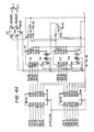
- FIG. 2 is the analog portion of the clock pulse generator comprising the VCO 10 and the operational amplifier (op amp) 11 that controls it.
- a clock pulse counter for facet zero will count clock pulses occurring between the start and end of scan. This count may be too high or too low, and will result, if necessary, in an input at the PUMP DOWN and PUMP UP inputs to amplifiers 12 and 13. These amplifiers are charge pumps and inject a positive or negative charge through isolation diodes 14, 15 and a resistor 16 to the signal input of the integrating op amp 11 with its integrating capacitor 17. The analog output is then coupled through adder 18 to control the frequency of the VCO 10.
- the second-order integrator comprises op amp 19 and capacitor 20. It receives the same input signals as the integrator 11 through isolation diodes 21, 22 and resistor 23, but the time constant is much longer because of the larger value of capacitor 20, and therefore, this integrator can track the slow change of the motor frequency.
- the output in coupled to the signal input of op amp 11 to compensate for the charge leakage there caused by the short time constant of that integrator.
- Diodes 24, 25, 26 create a two volt bias at the op amp I reference input, pin 3, so that a range of from zero to four volts can be accepted at the signal input pin 2.
- the adder 18 in addition to coupling the signal from op amp 11 to VCO 10, also adds to that signal a correction voltage for each facet.
- This correction voltage is generated in a circuit, described in more detail below, comprising a counter for counting clock pulses for each scan and for incrementing or decrementing a correction factor in a RAM if the count was too high or low, and a DAC for converting each RAM correction factor into a correction voltage for input to the adder 18.
- the circuit is designed so that a maximum of two percent error for each facet can be accommodated. In this way, op amp 11 tracks the motor frequency and adder 18 corrects for facet "signature" errors.
- the start-of-scan signal is used as the BIT CLK RESET input to amplifier 27 to produce a RESET signal which is coupled through transistor 28 to the VCO 10 as a start signal.
- the clock pulse generator is started synchronously with the start of scan.
- the novelty of this invention over the known prior art is the correction of each facet, through the addition of correction voltages at the adder 18.
- An additional point of novelty is the combination of the facet signature correction circuit with the leakage correction op amp 19. Without this leakage correction, facet zero would be offset from the remainder.
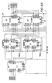
- the bit clock, BitClock is applied through gate e01a of Figure 4 to the bit counter comprising counter devices hl4b, hl4a, gl4 and f 14.
- the counter is first set to a predetermined value corresponding to the desired number of clocks per scan (in fact, the counter is set to its full count minus the number of clock pulses per scan). This predetermined value is loaded into the counter from a controller through latches e14 and d14. Then, during the scan, the counter is clocked up until it overflows, resulting in the EOLCount signal outputs at flip-flop f 16b.
- the counters are initially reset by the Bit ClockReset signal from gate g06a of Figure 3.
- the end of line count EOLCount is coupled from flip-flop fl6b to gates hOla and hOlb of Figure 3, along with the delayed reset ls50 to produce PUMPUP and PUMP DOWN signals at the outputs of gates hOla and hO1b, but only if the system is using facet zeroat the time (the Facet Zero signal is true at the input of gate h02a). Since the ls50 signal occurs at the actual end of scan and the EOLCount signal occurs when the predetermined number of clock pulses have been generated, which may be earlier or later than ls50, the PUMPUP and PUMPDOWN signals are variable in duration.
- the facet zero servo sequence is to load the desired count through registers e 14 and d 14 of Figure 4, count clock pulses in counter fl4, gl4, hl4a, and hl4b, produce therefrom an end-of-line count indication at flip flop fl6b, and finally produce at the output of gate hOla and hOlb of Figure 3 correction signals, PUMPUP and PUMPDOWN, which are used to modify the clock frequency as described and shown in Figure 2.
- This Figure 3 circuit is disabled for all other facets.
- Gates h03b and h03c receive the count signals EOLCount and produce therefrom correction signals for each facet, Increment or Decrement, which are used to modify each facet error count by one bit.
- a facet clock FacetInc is coupled through gate j03a to provide a clock to the counter 104 and is also coupled through flip-flop j04a to become the least significant output bit signal FacetAddress04 of the thirty - two bit facet counter.
- the remaining four signals FacetAddress00 through 03 are generated therefrom by counter 104.
- FacetAddress04 and the counter 104 carry output are combined in gate k04b and coupled through flip-flop j04b to produce the FacetZero signal used in the circuit of Figure 3.
- Figure 5 includes a circuit for producing a facet signature RAM write enable signal FacetWE which allows a one bit correction of the RAM of Figure 6, a digital to analog strobe signal D/AStrobe to allow a change of input for the digital analog converter U6 of Figure 7, and a facet counter 104 ( Figure 4) clock pulse, FacetInc.
- These signals are produced by the delayed line sync ls50 which is further delayed by counter i06, i07, to produce output signals from device i05 that are delayed out into the dead time between scans.
- Counter i06, i07 is set up to a count supplied from device h09 and then counted down by clock pulses generated of delay i09 and gate i08b which are implemented to oscillate to produce pulses.
- the carryout is coupled through gate 104a, latch i05 and gate j03c to produce the signals described above.
- the RAM devices 105, 106, k05, k06, j05, and j06 are addressed by the facet number, FacetAddress00 through 03, and store and output the correction value which is used by the DAC of Figure 7.
- these values are supplied through registers 109, k09, and j09 to the inputs of ALU devices 107, 108, k07, k08,j07, and j08.
- these values are either incremented or decremented by signals Decrement or Increment to correct each before being re-stored in the RAMs.
- Figure 7 is a schematic of the digital to analog converter U6 which converts the digital output of the RAMs, D/A 00 through D/A 11, coupled through registers U4 and U5, into an analog voltage, 2% ERROR, which is the input to adder 18 of Figure 2.
Landscapes
- Engineering & Computer Science (AREA)
- Multimedia (AREA)
- Signal Processing (AREA)
- Mechanical Optical Scanning Systems (AREA)
- Laser Beam Printer (AREA)
- Exposure Or Original Feeding In Electrophotography (AREA)
- Facsimile Scanning Arrangements (AREA)
- Control Of Electric Motors In General (AREA)
Applications Claiming Priority (2)
| Application Number | Priority Date | Filing Date | Title |
|---|---|---|---|
| US165813 | 1980-07-03 | ||
| US06/165,813 US4320420A (en) | 1980-07-03 | 1980-07-03 | Hybrid bit clock servo |
Publications (3)
| Publication Number | Publication Date |
|---|---|
| EP0043720A2 true EP0043720A2 (fr) | 1982-01-13 |
| EP0043720A3 EP0043720A3 (en) | 1982-04-07 |
| EP0043720B1 EP0043720B1 (fr) | 1984-10-03 |
Family
ID=22600587
Family Applications (1)
| Application Number | Title | Priority Date | Filing Date |
|---|---|---|---|
| EP81303059A Expired EP0043720B1 (fr) | 1980-07-03 | 1981-07-03 | Circuit de compensation d'erreur pour un générateur de signaux d'horloge |
Country Status (6)
| Country | Link |
|---|---|
| US (1) | US4320420A (fr) |
| EP (1) | EP0043720B1 (fr) |
| JP (1) | JPS5735472A (fr) |
| BR (1) | BR8104234A (fr) |
| CA (1) | CA1159550A (fr) |
| DE (1) | DE3166464D1 (fr) |
Cited By (3)
| Publication number | Priority date | Publication date | Assignee | Title |
|---|---|---|---|---|
| FR2550035A1 (fr) * | 1983-07-29 | 1985-02-01 | Dainippon Screen Mfg | Procede et systeme permettant de faire coincider plusieurs images reproduites, notamment dans un systeme de reproduction d'images a tambour |
| EP0618472A3 (fr) * | 1993-03-28 | 1995-10-11 | Scitex Corp Ltd | Un dispositif de balayage. |
| EP0691783A3 (fr) * | 1994-07-04 | 1996-04-10 | Fuji Xerox Co Ltd | Générateur d'horloge d'éléments d'image |
Families Citing this family (12)
| Publication number | Priority date | Publication date | Assignee | Title |
|---|---|---|---|---|
| US4559562A (en) * | 1983-08-16 | 1985-12-17 | Xerox Corporation | Microdeflector facet tracker for scanning system |
| EP0147835B1 (fr) * | 1983-12-28 | 1991-02-27 | Fuji Photo Film Co., Ltd. | Appareil d'analyse à faisceau lumineux |
| US4586057A (en) * | 1984-03-15 | 1986-04-29 | Minnesota Mining And Manufacturing Company | Compensation circuitry for a laser printer using a self-resonant scanner |
| US4622593A (en) * | 1984-05-29 | 1986-11-11 | Xerox Corporation | Polygon signature correction |
| US4639789A (en) * | 1984-05-29 | 1987-01-27 | Xerox Corporation | Raster scanner variable-frequency clock circuit |
| US4587531A (en) * | 1984-11-05 | 1986-05-06 | Eastman Kodak Company | Clock signal producing apparatus |
| US4635000A (en) * | 1985-11-12 | 1987-01-06 | Xerox Corporation | Temporal pixel clock synchronization system |
| US4694156A (en) * | 1986-02-14 | 1987-09-15 | Xerox Corporation | Pixel placement sensing arrangement using split detecting elements |
| EP0265845B1 (fr) * | 1986-10-29 | 1993-09-22 | Dainippon Screen Mfg. Co., Ltd. | Procédé et appareil pour la correction de la vacillation d'un miroir polygonal dans un appareil d'enregistrement d'images |
| US4888647A (en) * | 1987-12-21 | 1989-12-19 | Minolta Camera Kabushiki Kaisha | Image recording apparatus with improved SOS detection |
| US5248997A (en) * | 1991-10-28 | 1993-09-28 | Eastman Kodak Company | Facet reflectance correction in a polygon scanner |
| US5973574A (en) * | 1997-04-21 | 1999-10-26 | Eastman Kodak Company | Oscillator system with corrective frequency modulation |
Family Cites Families (12)
| Publication number | Priority date | Publication date | Assignee | Title |
|---|---|---|---|---|
| US3636250A (en) * | 1964-02-26 | 1972-01-18 | Andrew V Haeff | Apparatus for scanning and reproducing a three-dimensional representation of an object |
| GB1194226A (en) * | 1966-10-17 | 1970-06-10 | Texas Instruments Inc | Information Display Method and System. |
| US4040096A (en) * | 1972-11-27 | 1977-08-02 | Xerox Corporation | Flying spot scanner with runout correction |
| US3922485A (en) * | 1972-11-27 | 1975-11-25 | Xerox Corp | Flying spot scanner with scan detection |
| US4084197A (en) * | 1975-10-23 | 1978-04-11 | Xerox Corporation | Flying spot scanner with scan detection |
| JPS52108142A (en) * | 1976-03-08 | 1977-09-10 | Fuji Photo Film Co Ltd | Light beam scanning system |
| US4051538A (en) * | 1976-06-28 | 1977-09-27 | International Business Machines Corporation | Ink jet copier |
| US4158859A (en) * | 1977-07-25 | 1979-06-19 | Hazeltine Corporation | Automatic control of iris and clamping voltage in video signal generator |
| US4130838A (en) * | 1977-08-11 | 1978-12-19 | Xerox Corporation | Speed control apparatus for scanning system |
| US4151555A (en) * | 1977-11-25 | 1979-04-24 | The Mead Corporation | Optical scanning and encoding device |
| US4231070A (en) * | 1978-12-07 | 1980-10-28 | Texaco Inc. | High speed copying means and method |
| US4195316A (en) * | 1978-12-22 | 1980-03-25 | Pitney Bowes Inc. | Apparatus and method for correcting imperfection in a polygon used for laser scanning |
-
1980
- 1980-07-03 US US06/165,813 patent/US4320420A/en not_active Expired - Lifetime
-
1981
- 1981-05-13 CA CA000377527A patent/CA1159550A/fr not_active Expired
- 1981-06-23 JP JP9736981A patent/JPS5735472A/ja active Pending
- 1981-07-02 BR BR8104234A patent/BR8104234A/pt not_active IP Right Cessation
- 1981-07-03 EP EP81303059A patent/EP0043720B1/fr not_active Expired
- 1981-07-03 DE DE8181303059T patent/DE3166464D1/de not_active Expired
Cited By (5)
| Publication number | Priority date | Publication date | Assignee | Title |
|---|---|---|---|---|
| FR2550035A1 (fr) * | 1983-07-29 | 1985-02-01 | Dainippon Screen Mfg | Procede et systeme permettant de faire coincider plusieurs images reproduites, notamment dans un systeme de reproduction d'images a tambour |
| EP0618472A3 (fr) * | 1993-03-28 | 1995-10-11 | Scitex Corp Ltd | Un dispositif de balayage. |
| US5594556A (en) * | 1993-03-28 | 1997-01-14 | Scitex Corporation Ltd. | Scanner having a misalignment detector |
| EP0691783A3 (fr) * | 1994-07-04 | 1996-04-10 | Fuji Xerox Co Ltd | Générateur d'horloge d'éléments d'image |
| US5671069A (en) * | 1994-07-04 | 1997-09-23 | Fuji Xerox Co., Ltd. | Pixel clock generator |
Also Published As
| Publication number | Publication date |
|---|---|
| JPS5735472A (en) | 1982-02-26 |
| DE3166464D1 (en) | 1984-11-08 |
| CA1159550A (fr) | 1983-12-27 |
| EP0043720B1 (fr) | 1984-10-03 |
| EP0043720A3 (en) | 1982-04-07 |
| BR8104234A (pt) | 1982-03-23 |
| US4320420A (en) | 1982-03-16 |
Similar Documents
| Publication | Publication Date | Title |
|---|---|---|
| US4320420A (en) | Hybrid bit clock servo | |
| US5294944A (en) | Color image forming apparatus having means for properly superimposing image colors on each other | |
| US4622593A (en) | Polygon signature correction | |
| US4920430A (en) | Method of and apparatus for jitter correction of a polygon mirror in an image recording apparatus | |
| KR930003035B1 (ko) | 스캐너 모우터 회전 제어회로 | |
| EP1119185B1 (fr) | Circuit pour la correction de la fréquence de référence et de l'erreur entre facettes du miroir | |
| JP4336177B2 (ja) | 画素クロック生成装置、光走査装置及び画像形成装置 | |
| KR930000022B1 (ko) | 광 주사장치 | |
| EP0691783B1 (fr) | Générateur d'horloge d'éléments d'image | |
| JPH0231366B2 (fr) | ||
| EP0021831B1 (fr) | Circuit d'horloge pour signaux d'image et procédé de fonctionnement d'un dispositif de visualisation à trames | |
| JP3166311B2 (ja) | レーザースキャナ | |
| US4860237A (en) | Scan linearity correction | |
| US4639789A (en) | Raster scanner variable-frequency clock circuit | |
| US5115328A (en) | Beam scan type recording apparatus with electrically F theta correcting function | |
| US5059987A (en) | Synchronizing signal generating system | |
| US4803367A (en) | Light beam scanning apparatus employing beam modulation in accordance with the start of scan and end of scan signals | |
| US5164843A (en) | Scanner with a linearized vco pixel clock | |
| US5193013A (en) | Scanner with non-linearity compensating pixel clock | |
| JPS6342278A (ja) | 特性時間同期からの偏位を補償した媒体への情報の記録方法および装置 | |
| US6947515B2 (en) | Method for measuring the response of a voltage controlled oscillator | |
| US6529055B1 (en) | Method for adjusting the center frequency of a phase locked loop | |
| US6559978B1 (en) | Image reader | |
| US6160566A (en) | Registry adjusting device for laser beam printer | |
| JPS63132214A (ja) | ポリゴンミラ−のジツタ補正方法および装置 |
Legal Events
| Date | Code | Title | Description |
|---|---|---|---|
| PUAI | Public reference made under article 153(3) epc to a published international application that has entered the european phase |
Free format text: ORIGINAL CODE: 0009012 |
|
| AK | Designated contracting states |
Designated state(s): DE FR GB IT |
|
| PUAF | Information related to the publication of a search report (a3 document) modified or deleted |
Free format text: ORIGINAL CODE: 0009199SEPU |
|
| PUAL | Search report despatched |
Free format text: ORIGINAL CODE: 0009013 |
|
| AK | Designated contracting states |
Designated state(s): DE FR GB IT |
|
| D17D | Deferred search report published (deleted) | ||
| KL | Correction list |
Free format text: 82/03 |
|
| 17P | Request for examination filed |
Effective date: 19820601 |
|
| ITF | It: translation for a ep patent filed | ||
| GRAA | (expected) grant |
Free format text: ORIGINAL CODE: 0009210 |
|
| AK | Designated contracting states |
Designated state(s): DE FR GB IT |
|
| REF | Corresponds to: |
Ref document number: 3166464 Country of ref document: DE Date of ref document: 19841108 |
|
| ET | Fr: translation filed | ||
| PLBE | No opposition filed within time limit |
Free format text: ORIGINAL CODE: 0009261 |
|
| STAA | Information on the status of an ep patent application or granted ep patent |
Free format text: STATUS: NO OPPOSITION FILED WITHIN TIME LIMIT |
|
| 26N | No opposition filed | ||
| ITTA | It: last paid annual fee | ||
| PGFP | Annual fee paid to national office [announced via postgrant information from national office to epo] |
Ref country code: GB Payment date: 19980624 Year of fee payment: 18 |
|
| PGFP | Annual fee paid to national office [announced via postgrant information from national office to epo] |
Ref country code: FR Payment date: 19980709 Year of fee payment: 18 |
|
| PGFP | Annual fee paid to national office [announced via postgrant information from national office to epo] |
Ref country code: DE Payment date: 19980713 Year of fee payment: 18 |
|
| PG25 | Lapsed in a contracting state [announced via postgrant information from national office to epo] |
Ref country code: GB Free format text: LAPSE BECAUSE OF NON-PAYMENT OF DUE FEES Effective date: 19990703 |
|
| PG25 | Lapsed in a contracting state [announced via postgrant information from national office to epo] |
Ref country code: FR Free format text: THE PATENT HAS BEEN ANNULLED BY A DECISION OF A NATIONAL AUTHORITY Effective date: 19990731 |
|
| GBPC | Gb: european patent ceased through non-payment of renewal fee |
Effective date: 19990703 |
|
| PG25 | Lapsed in a contracting state [announced via postgrant information from national office to epo] |
Ref country code: DE Free format text: LAPSE BECAUSE OF NON-PAYMENT OF DUE FEES Effective date: 20000503 |
|
| REG | Reference to a national code |
Ref country code: FR Ref legal event code: ST |