EP0044155B1 - Synthétiseur de fréquences à verrouillage de phase modulé en fréquence - Google Patents
Synthétiseur de fréquences à verrouillage de phase modulé en fréquence Download PDFInfo
- Publication number
- EP0044155B1 EP0044155B1 EP81302907A EP81302907A EP0044155B1 EP 0044155 B1 EP0044155 B1 EP 0044155B1 EP 81302907 A EP81302907 A EP 81302907A EP 81302907 A EP81302907 A EP 81302907A EP 0044155 B1 EP0044155 B1 EP 0044155B1
- Authority
- EP
- European Patent Office
- Prior art keywords
- signal
- frequency
- phase
- modulation
- controlled oscillator
- Prior art date
- Legal status (The legal status is an assumption and is not a legal conclusion. Google has not performed a legal analysis and makes no representation as to the accuracy of the status listed.)
- Expired
Links
- 230000010363 phase shift Effects 0.000 claims description 100
- 238000012937 correction Methods 0.000 claims description 24
- 230000008878 coupling Effects 0.000 claims description 22
- 238000010168 coupling process Methods 0.000 claims description 22
- 238000005859 coupling reaction Methods 0.000 claims description 22
- 238000012546 transfer Methods 0.000 claims description 22
- 230000007423 decrease Effects 0.000 claims description 14
- 230000004044 response Effects 0.000 claims description 10
- 230000001747 exhibiting effect Effects 0.000 claims description 8
- 230000001419 dependent effect Effects 0.000 claims description 6
- 230000000737 periodic effect Effects 0.000 claims description 4
- 230000003247 decreasing effect Effects 0.000 claims description 3
- 230000005540 biological transmission Effects 0.000 claims description 2
- 238000012544 monitoring process Methods 0.000 claims 4
- 230000005669 field effect Effects 0.000 description 22
- 230000000694 effects Effects 0.000 description 21
- 238000013461 design Methods 0.000 description 19
- 230000006870 function Effects 0.000 description 17
- 239000003990 capacitor Substances 0.000 description 13
- 230000014509 gene expression Effects 0.000 description 11
- 238000000034 method Methods 0.000 description 9
- 230000009467 reduction Effects 0.000 description 6
- 230000002829 reductive effect Effects 0.000 description 5
- 238000010897 surface acoustic wave method Methods 0.000 description 5
- 230000001052 transient effect Effects 0.000 description 4
- 230000003190 augmentative effect Effects 0.000 description 3
- 230000008859 change Effects 0.000 description 3
- 238000010586 diagram Methods 0.000 description 3
- 238000012986 modification Methods 0.000 description 3
- 230000004048 modification Effects 0.000 description 3
- 230000035945 sensitivity Effects 0.000 description 3
- 230000003213 activating effect Effects 0.000 description 2
- 238000004891 communication Methods 0.000 description 2
- 230000000295 complement effect Effects 0.000 description 2
- 239000013078 crystal Substances 0.000 description 2
- 238000001514 detection method Methods 0.000 description 2
- 230000000670 limiting effect Effects 0.000 description 2
- 238000012545 processing Methods 0.000 description 2
- 101000863856 Homo sapiens Shiftless antiviral inhibitor of ribosomal frameshifting protein Proteins 0.000 description 1
- XUIMIQQOPSSXEZ-UHFFFAOYSA-N Silicon Chemical compound [Si] XUIMIQQOPSSXEZ-UHFFFAOYSA-N 0.000 description 1
- 238000013459 approach Methods 0.000 description 1
- 238000010420 art technique Methods 0.000 description 1
- 230000004888 barrier function Effects 0.000 description 1
- 230000006399 behavior Effects 0.000 description 1
- 230000008901 benefit Effects 0.000 description 1
- 238000004364 calculation method Methods 0.000 description 1
- 238000006243 chemical reaction Methods 0.000 description 1
- 230000001427 coherent effect Effects 0.000 description 1
- 230000002301 combined effect Effects 0.000 description 1
- 150000001875 compounds Chemical class 0.000 description 1
- 238000010276 construction Methods 0.000 description 1
- 230000003111 delayed effect Effects 0.000 description 1
- 230000007613 environmental effect Effects 0.000 description 1
- 230000006872 improvement Effects 0.000 description 1
- 230000000977 initiatory effect Effects 0.000 description 1
- 238000003780 insertion Methods 0.000 description 1
- 230000037431 insertion Effects 0.000 description 1
- 230000002452 interceptive effect Effects 0.000 description 1
- 238000009533 lab test Methods 0.000 description 1
- 230000007774 longterm Effects 0.000 description 1
- 238000004519 manufacturing process Methods 0.000 description 1
- 238000007620 mathematical function Methods 0.000 description 1
- 230000007246 mechanism Effects 0.000 description 1
- 238000011022 operating instruction Methods 0.000 description 1
- 230000010355 oscillation Effects 0.000 description 1
- 230000036961 partial effect Effects 0.000 description 1
- 230000008439 repair process Effects 0.000 description 1
- 230000008672 reprogramming Effects 0.000 description 1
- 229910052710 silicon Inorganic materials 0.000 description 1
- 239000010703 silicon Substances 0.000 description 1
- 238000001228 spectrum Methods 0.000 description 1
- 230000007704 transition Effects 0.000 description 1
Images



Classifications
-
- H—ELECTRICITY
- H03—ELECTRONIC CIRCUITRY
- H03C—MODULATION
- H03C3/00—Angle modulation
- H03C3/02—Details
- H03C3/09—Modifications of modulator for regulating the mean frequency
- H03C3/0908—Modifications of modulator for regulating the mean frequency using a phase locked loop
- H03C3/0966—Modifications of modulator for regulating the mean frequency using a phase locked loop modulating the reference clock
-
- H—ELECTRICITY
- H03—ELECTRONIC CIRCUITRY
- H03C—MODULATION
- H03C3/00—Angle modulation
- H03C3/02—Details
- H03C3/09—Modifications of modulator for regulating the mean frequency
- H03C3/0908—Modifications of modulator for regulating the mean frequency using a phase locked loop
- H03C3/0941—Modifications of modulator for regulating the mean frequency using a phase locked loop applying frequency modulation at more than one point in the loop
-
- H—ELECTRICITY
- H03—ELECTRONIC CIRCUITRY
- H03C—MODULATION
- H03C3/00—Angle modulation
- H03C3/02—Details
- H03C3/09—Modifications of modulator for regulating the mean frequency
- H03C3/0908—Modifications of modulator for regulating the mean frequency using a phase locked loop
- H03C3/095—Modifications of modulator for regulating the mean frequency using a phase locked loop applying frequency modulation to the loop in front of the voltage controlled oscillator
-
- H—ELECTRICITY
- H03—ELECTRONIC CIRCUITRY
- H03L—AUTOMATIC CONTROL, STARTING, SYNCHRONISATION OR STABILISATION OF GENERATORS OF ELECTRONIC OSCILLATIONS OR PULSES
- H03L7/00—Automatic control of frequency or phase; Synchronisation
- H03L7/06—Automatic control of frequency or phase; Synchronisation using a reference signal applied to a frequency- or phase-locked loop
- H03L7/08—Details of the phase-locked loop
- H03L7/10—Details of the phase-locked loop for assuring initial synchronisation or for broadening the capture range
- H03L7/113—Details of the phase-locked loop for assuring initial synchronisation or for broadening the capture range using frequency discriminator
-
- H—ELECTRICITY
- H03—ELECTRONIC CIRCUITRY
- H03L—AUTOMATIC CONTROL, STARTING, SYNCHRONISATION OR STABILISATION OF GENERATORS OF ELECTRONIC OSCILLATIONS OR PULSES
- H03L7/00—Automatic control of frequency or phase; Synchronisation
- H03L7/06—Automatic control of frequency or phase; Synchronisation using a reference signal applied to a frequency- or phase-locked loop
- H03L7/16—Indirect frequency synthesis, i.e. generating a desired one of a number of predetermined frequencies using a frequency- or phase-locked loop
- H03L7/18—Indirect frequency synthesis, i.e. generating a desired one of a number of predetermined frequencies using a frequency- or phase-locked loop using a frequency divider or counter in the loop
- H03L7/183—Indirect frequency synthesis, i.e. generating a desired one of a number of predetermined frequencies using a frequency- or phase-locked loop using a frequency divider or counter in the loop a time difference being used for locking the loop, the counter counting between fixed numbers or the frequency divider dividing by a fixed number
- H03L7/187—Indirect frequency synthesis, i.e. generating a desired one of a number of predetermined frequencies using a frequency- or phase-locked loop using a frequency divider or counter in the loop a time difference being used for locking the loop, the counter counting between fixed numbers or the frequency divider dividing by a fixed number using means for coarse tuning the voltage controlled oscillator of the loop
-
- H—ELECTRICITY
- H03—ELECTRONIC CIRCUITRY
- H03C—MODULATION
- H03C2200/00—Indexing scheme relating to details of modulators or modulation methods covered by H03C
- H03C2200/0004—Circuit elements of modulators
- H03C2200/0029—Memory circuits, e.g. ROMs, RAMs, EPROMs, latches, shift registers
-
- H—ELECTRICITY
- H03—ELECTRONIC CIRCUITRY
- H03C—MODULATION
- H03C2200/00—Indexing scheme relating to details of modulators or modulation methods covered by H03C
- H03C2200/0037—Functional aspects of modulators
- H03C2200/005—Modulation sensitivity
-
- H—ELECTRICITY
- H03—ELECTRONIC CIRCUITRY
- H03C—MODULATION
- H03C2200/00—Indexing scheme relating to details of modulators or modulation methods covered by H03C
- H03C2200/0037—Functional aspects of modulators
- H03C2200/005—Modulation sensitivity
- H03C2200/0054—Filtering of the input modulating signal for obtaining a constant sensitivity of frequency modulation
Definitions
- This invention relates to frequency modulated signal sources. More particularly, this invention relates to signal sources for supplying a frequency modulated signal at any one of numerous selectable carrier frequencies.
- a signal source must provide a frequency modulated signal at a relatively large number of carrier frequencies that extend over a substantial frequency range and the problems associated with achieving a circuit design that satisfactorily realizes the above-noted linear modulation characteristic are greatly increased.
- inherent nonlinearities in the modulation characteristics associated with practical circuit realizations cause distortion of the modulated signal.
- achieving an acceptable distortion level not only requires that the system modulation characteristic be substantially linear but also requires that the modulation characteristic be substantially invariant relative to the set of carrier frequencies of interest. Because all components and networks exhibit at least a certain degree of frequency dependence, prior art signal sources that provide satisfactory (e.g., low-distortion) frequency modulation over a relatively wide range of carrier frequencies are often relatively complex.
- signal sources that serve as laboratory instrumentation and signal sources utilized in channelized communication equipment often must supply frequency modulated signals wherein the carrier frequency is a precise, selected value.
- Such signal sources must not only additionally exhibit substantial long-term and short-term frequency stability, but must often meet demanding noise requirements with respect to stochastic internal circuit noise and coherent noise such as that caused by nonlinear circuit operation and bias supply ripple.
- remote programming or signal selection via a digitally encoded or analog control signal is often a desirable or necessary feature.
- Prior art attempts to provide frequency modulated rf signal sources basically include circuitry wherein the modulating signal directly controls the operating frequency of various types or classes of tune oscillators and arrangements wherein the carrier frequency is produced by a conventional oscillator arrangement and frequency modulation is induced by subsequent processing of the carrier signal.
- those circuits which directly control the frequency of a tunable signal source include variable reactance devices which are electrically coupled to the resonant circuit that determines the frequency of oscillation wherein the modulating signal is coupled to the variable reactance and thereby controls the signal frequency.
- the frequency of an active oscillator circuit is established by a mechanically-tuned resonant cavity and frequency modulation is induced by supplying the modulating signal to a varactor diode that is coupled to the resonant cavity. Since the coupling between the varactor diode and the resonant cavity does not detrimentally affect the relatively high Q of the cavity, this type of arrangement exhibits a relatively high signal to noise ratio and permits selection of precise carrier frequencies.
- selection of each desired carrier frequency requires manual adjustment of the mechanically-tuned cavity and concomittant adjustment of the electrical coupling between the varactor diode in order to provide a relatively constant modulation characteristic at each frequency of interest.
- such an arrangement may require fairly complex mechanical tuning devices. Further, because of the mechanical tuning requirement, it may not be possible to change such a signal source between accurately defined carrier frequencies as rapidly as desired or necessary and remote frequency programming is often either impractical or requires a complex control mechanism.
- Arrangements in which a selectable frequency carrier signal is generated by a conventional variable frequency oscillator and frequency modulated within subsequent circuit stages are typified by systems in which a signal at the desired carrier frequency is supplied by a first signal source and mixed or heterodyned with a frequency modulated signal that is obtained by modulating a second signal source which operates at a substantially invariant center frequency.
- the heterodyned signal is band-pass filtered, the necessary nonlinear characteristic of the mixing stage of such a system causes the generation of substantial spurious signal components.
- systems of this type that provide carrier frequencies extending over a relatively large frequency range (e.g., one octave or more) are relatively complex and costly.
- frequency synthesizers In situations that require remote frequency programming to enable selection of a desired carrier frequency from a large number of signal frequencies, signal sources that are commonly referred to as frequency synthesizers are often employed and several arrangements have been proposed for frequency modulating various types of frequency synthesizers.
- VCO voltage controlled oscillator
- phase-locked loop networks are designed to exhibit a relatively wide bandwidth and the phase-locked loop operates to eliminate phase and frequency perturbations occurring at rates within the loop bandwidth, it has been necessary to develop various circuit arrangements for satisfactorily phase or frequency modulating phase-locked systems.
- One approach to frequency modulating such a system in effect combines two modulation paths, the first of which accommodates fm rates within the bandwidth of the phase-locked loop and the second of which accommodates fm rates greater than the phase-locked loop bandwidth.
- modulation signals at fm rates within the bandwidth of the phase-locked loop modulate the oscillator that supplies the reference signal and modulation signals at fm rates outside of the bandwidth of the phase-locked loop are coupled to the frequency control terminal of the phase-locked loop voltage controlled oscillator.
- a second arrangement of this type also utilizes frequency modulation of the phase-locked loop voltage controlled oscillator for modulation signals outside the phase-locked loop bandwidth and accommodates fm rates within the phase-locked loop bandwidth by phase modulating the phase-locked loop phase detector.
- modulation signals at rates less than the crossover frequency of the phase-locked loop are typically coupled to the input terminal of the loop filter via a conventional integrator circuit.
- the low noise signal source disclosed in U.S. patent application Serial No. 168,065 of Donald G. Meyer, entitled “Controlled Frequency Source Apparatus Including a Feedback Path for the Reduction of Phase Noise”, filed 14th July 1980 and corresponding to our EPC Patent Application 81302905.5 (EP-A-44153) filed on the same day as this application provides a phase-locked loop having remote signal selection capabilities, a frequency range of one octave or more, and substantially less phase noise than previously realizable phase-locked loop systems.
- the frequency modulation problems associated with more conventional prior art phase-locked loop frequency synthesizers are not overcome or alleviated by the arrangement disclosed in the referenced patent application by Meyer, but, in fact, become more complex.
- the low noise programmable divide-by-N phase-locked loop arrangements disclosed in the Meyer application not only include a feedback path for establishing and maintaining phase-lock at the selected signal frequency, but also include a second feedback path that reduces phase noise by, in effect, demodulating the VCO output signal and supplying negative feedback that is proportional to VCO phase noise to the VCO frequency control terminal.
- This additional feedback path includes a frequency discriminator of the type which includes a time delay network (e.g., a surface acoustic wave (SAW) delay device or a coaxial cable) that is serially interconnected between one input port of a phase detector and the output terminal of the VCO.
- a time delay network e.g., a surface acoustic wave (SAW) delay device or a coaxial cable
- Variable phase shifting apparatus included in one or both of the phase detector input paths, is automatically controlled in response to the signal provided by the phase detector and/or the system frequency selection signal so as to maintain the phase detector output signal substantially equal to zero at each selected. frequency of operation (i.e., at phase-lock).
- the frequency discriminator effectively tracks the phase-locked loop to provide negative feedback to the VCO frequency control terminal and; by properly configuring the system, low phase noise is attained without significantly altering frequency selection (tuning) characteristics.
- US-A-4123719 discloses a frequency modulated signal source comprising a modulated phase-locked loop system which comprises controlled oscillator means having an output terminal and a frequency control terminal, the controlled oscillator means applying a signal to the output terminal at a frequency determined by the magnitude of a frequency control signal applied to the frequency control terminal; feedback means responsive to the signal supplied by the controlled oscillator means to the output terminal thereof for supplying a feedback signal to the frequency control terminal of the controlled oscillator means, the feedback means including one feedback path which includes a frequency discriminator network, the frequency discriminator network including phase detector means having an output port and first and second input ports, coupler means for coupling the signals supplied to the output terminal of the controlled oscillator means to the first and second input ports of the phase detector means, time delay means exhibiting a time delay of T , the time delay means being connected to delay the signal coupled to one of the first and second input ports of the phase detector means, and signal coupling means for coupling the signal supplied by the frequency discriminator network to the frequency control terminal of the controlled oscill
- the feedback signal that is supplied to the frequency control terminal of the controlled oscillator means is used as an error signal which is an indication of frequency non-linearity of the wave form of the periodic signal generated by the controlled oscillator means, that error signal being used to correct the frequency non-linearity of that wave form.
- a frequency modulated signal source comprising a modulated phase-locked loop system which comprises:
- said feedback means includes another feedback path responsive to the signal supplied by said controlled oscillator means to said output terminal thereof for supplying a feedback signal to said frequency control terminal of said controlled oscillator means, that other feedback path including means for phase-locking said controlled oscillator means at a selected carrier frequency, said means for phase-locking said controlled oscillator means including a second phase detector means having an output port and first and second input ports, said first input port of said second phase detector means being coupled to said output terminal of said controlled oscillator means for receiving a signal at a frequency dependent on the frequency of the signal being supplied by said controlled oscillator means, said second input port of said second phase detector means being connected for receiving an applied reference signal, said output port of said second phase detector means being connected for coupling a signal to said frequency control terminal of said controlled oscillator means; and said second modulation path is configured and arranged to inject at least a portion of an applied modulation signal into said other feedback path to modulate said second phase detector means;
- modulated phase-locked loop system also comprises:
- a preferred embodiment of this invention comprises a low noise signal source of the general type disclosed in the previously-referenced patent application of Meyer which is arranged to, in effect, divide the range of output frequencies into a set of relatively narrow, contiguous subbands and which is augmented with circuitry that automatically adjusts the level of an applied modulation signal so that a given modulation level provides a predetermined frequency deviation at the center frequency (or some other convenient point) of each subband. Circuitry is also included to compensate for frequency-dependent gain variations throughout the subbands to thereby provide accurate, low distortion frequency modulation over the entire output range of the signal source.
- a frequency modulated signal in which this invention is embodied is arranged to prevent the modulation signal from reaching portions of the noise-reducing circuit that maintain the average value of the frequency discriminator phase detector output signal substantially equal to zero at the desired carrier frequency.
- the preferred phase-locked loop embodiments of the invention include circuitry for improving signal acquision or tuning time and ensuring that the system is unconditionally stable under all possible operating states including turn on and transient conditions.
- the carrier signal is supplied by a signal source configured in accordance with the border aspects of the previously-referenced patent application of Meyer so that a portion of the output signal produced by a voltage controlled oscillator (VCO) is coupled to the VCO frequency control terminal via a feedback path which includes a frequency discriminator network and an amplifier circuit.
- the frequency discriminator network includes a phase detector network wherein the VCO output signal is coupled to both input ports of the phase detector with a time delay network being interconnected in one of the circuit paths to cause a phase difference ⁇ between the phase detector input signals, where W is the frequency of the VCO in radians/second and ⁇ is the time delay.
- variable phase shifter of each disclosed embodiment exhibits a phase shift range of at least 2 7 r/k with the amount of phase shift inserted in the system being determined by an analog signal that is supplied by a phase shifter control circuit which is interconnected between the output of the frequency discriminator and a control terminal of the variable phase shifter.
- the output voltage vs frequency characteristic of the discriminator is substantially equal to where K d is a constant, ⁇ e is the phase shift provided by the variable phase shifter and the algebraic sign of the phase shift provided by the stepped phase shifter depends on which of the two phase detector input paths includes the stepped phase shift.
- Each of the disclosed embodiments of the invention include a frequency selective feedback path that causes the system to operate as a phase-locked loop frequency synthesizer with both the frequency selection path and the noise-reducing discriminator path being arranged to meet constraints set forth in the previously-mentioned patent application of Meyer that are necessary to achieve maximum phase noise performance and conventional phase-locked loop tuning capabilities.
- each embodiment of the present invention couples a first modulation signal into the noise-reducing discriminator path to modulate the discriminator and a second modulation signal to an additional VCO (e.g., a crystal-controlled reference voltage controlled oscillator), that provides the phase-locked loop reference signal.
- the first modulation signal is thus summed with the loop feedback and, because of the high pass characteristics of the phase-locked loop is primarily effective at frequencies outside the effective loop bandwidth. Since the system VCO effectively tracks the reference oscillator for all frequencies within the phase-locked loop bandwidth, the second modulation signal provides low frequency modulation, with the combined effect of the two modulation signals ideally providing a flat frequency response that is independent of loop cutoff frequency.
- Maintaining frequency modulation that is a faithful reproduction of the modulation source through use of the above-discussed two modulation components requires proper delay equalization of the modulating signals and, more importantly, requires that the modulation coefficients associated with each modulation path are relatively invariant over the range of carrier frequencies being employed. In this respect, relatively constant modulation coefficients are attained over a substantial frequency band by compensation of the modulation signals on the basis of the carrier frequency and the subband with which that carrier frequency is associated.
- the output frequency of the VCO is related to the loop reference frequency by N, where N denotes the frequency division factor for the phase-locked loop, the modulation sensitivity for frequencies below the loop cutoff frequency is proportional to N.
- Compensation of the modulation component within the loop bandwidth is effected by multiplying the modulation component by 1/N, whereas compensation of the modulation component for modulation rates greater than the loop bandwidth utilizes a separate multiplicative compensation factor for each of the subbands that comprise the system bandwidth.
- the compensation or equalization factors associated with the subbands of one particular realization of the invention will not be identical to those required for another realization utilizing the same circuit arrangement.
- the discriminator equalization characteristics are determined for each unit that is constructed and provision is made for reestablishing the compensation factors upon replacement of system components within the discriminator path or should recalibration become necessary.
- the compensation factors are stored in an erasable random access memory (EPROM) within a conventional microprocessor arrangement that is activated by the system frequency selection signal.
- the microprocessor determines both the value of N and the subband associated with each particular selected frequency and addresses the correction factor stored EPROM for the subband associated with the selected frequency.
- digitally-encoded signals representing both N and the stored correction factor are coupled to the digital signal ports of multiplying-type digital-to-analog converters (DAC's) having the analog input terminals thereof connected for receiving the modulation signal.
- DAC's multiplying-type digital-to-analog converters
- the output terminals of the respective DAC's are coupled to the frequency control terminal of the voltage-controlled reference oscillator and to the gain unit of the previously-discussed noise-reducing discriminator feedback path.
- the discriminator characteristics are maintained substantially constant throughout each of the subbands by judicious impedance matching and by a circuit arrangement that compensates the signal within the noise-reducing discriminator path so as to maintain a relatively constant level at the signal (linear) input port of a doubly-balanced mixer, which serves as the phase detector of the noise-reducing discriminator feedback path.
- the presently preferred embodiment of the invention includes a circuit arrangement for accessing the proper frequency subband while simultaneously ensuring that the system is unconditionally stable each time the system is initially energized or a new frequency is selected that lies within a different subband.
- this signal acquisition circuitry includes a voltage comparator that activates a monostable multivibrator each time the system is tuned to a frequency that corresponds to the uppermost or lowermost frequency of a subband.
- the monostable multivibrator activates switching devices which attenuate the feedback signal supplied by the discriminator and simultaneously controls the system band pass so as to maintain a substantially constant loop bandwidth.
- the signal provided by the monostable multivibrator preferably activates an additional switch that interrupts (removes) the modulation signal to prevent modulation from reaching and interfering with the signal controlling the discriminator path variable phase shifter during each signal acquisition.
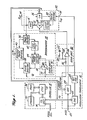
- the basic arrangement of this invention includes a low noise phase-locked loop system that is configured in accordance with the previously-mentioned patent application of Donald L. Meyer; a modulation compensator unit 12, which is responsive to an applied modulation signal and supplies two separate modulation signals to different circuit nodes within the low noise phase-locked loop; and a controller 14, which controls the operation of both the phase-locked loop and modulation compensator 12 on the basis of an applied frequency selection signal.
- the arrangement of Figure 1 provides a wide- band signal source wherein the system bandwidth is, in effect, partitioned into a plurality of contiguous subbands, having modulation characteristics that differ from one another because of component tolerances and other practical considerations.
- controller 14 determines the appropriate frequency subband and activates the low noise phase-locked loop to access that particular subband and, more specifically, the particular desired frequency within the accessed subband.
- controller 14 supplies modulation compensator 12 with two correction signals which are dependent upon the frequency selected and the subband associated with that frequency. These two correction signals establish the level of the two modulation components that are coupled to the phase-locked loop so as to substantially eliminate the differences between the modulation characteristics of the various subbands and effect a relatively constant deviation ratio at all carrier frequencies within the range of the phase-locked loop system.
- the low phase noise phase-locked loop portion of the embodiment depicted in Figure 1 includes a voltage controlled oscillator (VCO) 16 that is augmented with two feedback paths wherein the first feedback path includes a discriminator network 18 for reducing phase noise generated within VCO 16 and the second feedback path, in effect, configures the thusly-modified VCO 16 into a phase-locked loop system of the type frequently used as a frequency synthesizer. More specifically, in the illustrative embodiment of Figure 1, discriminator 18 of the noise-reducing feedback path is connected in cascade with a gain unit 20 and couples negative feedback from the VCO output terminal to a VCO frequency control terminal 22 via a conventional summing unit 24.
- VCO voltage controlled oscillator
- the second feedback path (typically referred to herein as the frequency selection feedback path) includes a programmable frequency divider 26, which is connected between the output terminal of VCO 16 and one input port of a phase detector 28, and a low-pass filter network 30 that is connected between the output port of phase detector 28 and the second input port of summing unit 24.
- the above-mentioned arrangement of VCO 16, frequency divider 26, phase detector 28 and filter 30 form a conventional programmable divide-by-N phase-locked loop system wherein the frequency of the signal provided by VCO 16 to the system output terminal 34 is Nf, ef , where N is the divisor of frequency divider 26 and f ref is the frequency of a reference signal that is coupled to the second input port of phase detector 28 (via terminal 35 in Figure 1).
- the divisor N is coupled to frequency divider 26 as a conventional digitally-encoded binary signal.
- discriminator 18 of the noise-reducing feedback path includes a conventional power splitter 36 which divides the signal provided by VCO 16 between two circuit paths that are connected to the input ports of a phase detector 38. Since one of the circuit paths includes a stepped phase shifter 40 and the second circuit path includes a time delay unit 42 and a variable phase shifter 44 that are connected in cascade with one another, it can be shown that the phase difference between the signals supplied to phase detector 38 is equal to where ⁇ is equal to the frequency of the signal supplied by VCO 16 in radians/second, T is the time delay associated with time delay unit 42 (in seconds) and ⁇ e and ⁇ s are respectively equal to the phase shift provided by variable phase shifter 44 and stepped phase shifter 40 (in radians).
- phase detector 38 is of the type conventionally employed in phase-locked loop circuits (i.e., a doubly-balanced signal mixer or one of the various conventional devices that approximate an ideal multiplier circuit), it can be recognized that the signal V d , provided to gain unit 20 by phase detector 38 is given by the expression
- Discriminator 18 also includes a phase shifter control unit 46 which receives the signal provided by phase detector 38 (V d ) and supplies a signal to a control port of variable phase shifter 44 to thereby establish the phase shift ⁇ e .
- the phase shift O e provided by variable phase shifter 44 is substantially equal to K s V P , where Vp is the signal provided by phase shifter control 46, and in conjunction with the phase shift provided by stepped phase shifter 40 causes the signal, V d , provided by phase detector 38 to be substantially equal to zero at each frequency selected through operation of the frequency selection loop.
- one arrangement for realizing a satisfactory phase shifter control 46 which provides a suitable dc control signal to variable phase shifter 44 is a conventional integrator circuit including an operational amplifier 48, an input resistor 50 and a feedback capacitor 52.
- the output signal provided by phase detector 38 of discriminator 18 is connected to a first input terminal of an operational amplifier 54 of the depicted gain unit 20 via a resistor 56.
- a feedback network which includes a resistor 58 that is connected in parallel with serially-connected resistor 60 and capacitor 62 is connected between the output and first input terminal of operational amplifier 54.
- the second input terminal of operational amplifier 54 receives a signal from modulation compensator 12 that establishes modulation at rates outside the phase-locked loop bandwidth and the output terminal of operational amplifier 54 is connected to the first input port of summing unit 24 to thereby couple a combined noise reduction-modulation signal into the phase-locked loop system.
- phase detector 28 and filter 30, which form the frequency selection feedback path for phase-locking VCO 16 to the reference signal supplied to terminal 35, low noise operation of the circuit of Figure 1 is accomplished while simultaneously maintaining conventional phase-locked loop tuning characteristics if the circuit components of the depicted arrangement are selected so that where ⁇ 3 is equal to the bandwidth of the depicted phase-locked loop arrangement when the noise-reducing feedback path is open-circuited. That is, ⁇ 3 corresponds to the bandwidth of the conventional phase-locked loop contained within dashed outline 32, which is known to be K ⁇ K ⁇ /N, where K ⁇ is the transfer constant associated with phase detector 28.
- phase noise is: (a) improved by a factor substantially equal to Go for all frequencies that are offset from the frequency of VCO 16 by less than ⁇ 0 ; (2) improved by a factor of less than Go for frequencies greater than ⁇ 0 with the noise performance being identical to a conventionally- arranged system at ⁇ 0 G 0 ; and, (3) substantially identical to that of a conventional phase-locked loop system for frequencies greater than woGo.
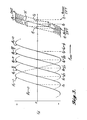
- the tuning properties and basic modulation characteristics of embodiment depicted in Figure 1 can be understood with reference to Figures 2 and 3, which depict signal diagrams that define the system discriminator characteristic, i.e., the signal V d that is supplied by discriminator 18 of the noise-reducing feedback path as a function of the frequency of VCO 16.
- Figure 2 illustrates the amplitude of the signal V d as a function of the frequency of VCO 16 when the noise-reducing feedback path is open-circuited to prevent feedback from reaching VCO 16 (e.g., the output of phase detector 38 is disconnected from gain unit 20) and the phase shift provided by stepped phase shifter 40 and variable phase shifter 44 is maintained at zero radians.
- the zero-phase characteristic of Figure 2 corresponds to the transfer characteristic of a conventional frequency discriminator that is commonly used to stabilize or lock an oscillator to a desired single frequency that corresponds to a selected zero crossover within a negative-going or positive-going portion of the depicted transfer characteristic.
- the arrangement of Figure 1 would operate as a discriminator stabilized signal source that would be stable only when the VCO was tuned to a frequency that corresponds to a zero crossover within a positive-going portion of the discriminator characteristic ((4n-1)/(4 ⁇ ), where n is a positive real integer) or a zero crossover within a negative-going portion of the discriminator characteristic (i.e., (4n-3)/(4 T )).
- circuit operation corresponds to that of a prior art discriminator-stabilized oscillator arrangement wherein an increase in the frequency of the signal supplied by VCO 16 causes discriminator 18 to supply a positive output signal and a decrease in the VCO frequency causes discriminator 18 to supply a negative output signal.
- VCO 16 By properly connecting such a feedback signal to the frequency control terminal of the VCO, e.g., by arranging gain unit 20 to provide inverting operation, negative feedback is provided that automatically returns the VCO to the selected frequency (4n-1 )/(4 ⁇ ).
- the frequency interval between zero crossings of the discriminator zero-phase characteristic is 1/ T
- the frequency interval or band defined between two crossovers within positive-going portions of the discriminator zero-phase characteristic (or negative-going portions) is effectively subdivided into k contiguous subbands through operation of stepped phase shifter 40.
- the frequency interval between f a and f b is divided into four subbands, each defining 1/(4 T ) hertz of the system bandwidth.
- variable phase shifter 44 must provide a phase shift over a range extending at least between -n/k radians and + 7 r/k radians if discriminator 18 of the arrangement depicted in Figure 1 is to provide a zero output signal at any selected frequency (i.e., in order to cause a zero crossover of the discriminator characteristic to occur at any frequency that lies within each of the subbands).
- a positive phase shift, ⁇ e causes each zero crossing of the discriminator characteristic to, in effect, shift upwardly in frequency whereas negative ⁇ e causes each zero crossing to occur at a corresponding lower frequency.
- phase shifter control unit 46 of Figure 1 is a conventionally arranged operational amplifier integrator circuit having a negative transfer characteristic, the gain constant of variable phase shifter 44 (i.e., K s ) must also be negative.
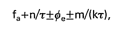
- the system can be tuned to any frequency Nf ref by selecting a value of m which produces a stepped, phase shift ⁇ s that causes a zero crossover of the discriminator characteristic to occur at a frequency that is within + 7 r/k of the selected frequency.
- This results in a phase detector output signal V d that, in turn, drives variable phase shifter 44 (via phase shifter control unit 46) in a manner which inserts additional phase shift O e that reduces the magnitude of the discriminator output signal V d until V d O.
- VCO 16 is caused to operate at a frequency substantially equal to Nf ref and the noise-reducing discriminator loop causes a zero crossing of the discriminator characteristic to occur at the selected frequency.
- the depicted modulation compensator 12 includes two conventional mutliplying-type digital-to-analog converter units (DAC's) 64 and 66 having the analog input terminals thereof commonly connected for receiving a modulation signal that is applied to a terminal 69.
- DAC's digital-to-analog converter units
- the digitally-encoded input signal to DAC 64 and DAC 66 is supplied by controller 14 and provides compensation for various factors that would otherwise cause FM inaccuracy.
- the signal provided by DAC 66 is coupled to the frequency control terminal of a voltage-controlled reference oscillator 68 having its output terminal connected to the reference frequency terminal 35 of the phase-locked loop arrangement.
- Reference oscillator 68 is preferably a voltage-controlled crystal oscillator and the frequency deviation ⁇ f of VCO 16 when the signal provided by reference oscillator 68 is injected into the input port of phase detector 28 is substantially equal to D 1 K x N, where D 1 is the gain or "weighting factor" effected by DAC 66 and the modulation coefficient of reference oscillator 68 is K X .
- the signal supplied by DAC 64 is coupled to one input terminal of operational amplifier 54 of gain unit 20.
- a modulation component proportional to D 2 ⁇ V, where D 2 is the gain or weighting factor of DAC 64, is injected into the noise-reducing feedback path so that the discriminator characteristic is utilized to effect modulation at frequencies outside the loop bandwidth ( ⁇ 3 /G 0 ).
- the discriminator characteristic denoted by the numeral 75 defines system operation relative to modulation components outside the loop bandwidth in that all signal variations coupled to the input terminal of operational amplifier 54 in Figure 1 cause a corresponding signal change to be coupled to the VCO frequency control terminal via summing unit 24.
- a periodic, symmetric modulation component e.g., a sinusoid
- V maximum amplitude of V
- the harmonic distortion encountered in the modulated signal depends on the linearity of the transfer characteristic.
- the deviation ratio is determined by the slope of the modulation characteristic and, if a constant deviation ratio is to be maintained over the full range of carrier frequencies supplied by the system, a constant slope must be maintained over the same range of frequencies.
- each of the indicated circuits or components within discriminator 18 exhibits phase and amplitude characteristics that vary with frequency.
- the positive-going (or, alternatively negative-going) portions of the discriminator input frequency to output voltage characteristic do not exhibit identical slope.
- neither the amplitude or delay characteristics of actual realizations of the depicted discriminator 18 are continuous relative to frequency because of the above-discussed operation of the stepped phase shifter 40 in dividing the system bandwidth into subbands which, in effect, position zero crossovers of the discriminator characteristic curve so that a modulation slope is provided at any selected frequency.
- Controller 14 of Figure 1 includes means for determining the subband associated with each selected frequency and, based on such information, supplies a digitally-encoded error correction signal to DAC 64 to adjust the modulation coupled to gain unit 20 in a manner which compensates for changes in the slope of the modulation transfer characteristic associated with a predetermined frequency within that particular subband (e.g., the center frequency of the subband).
- controller 14 supplies a digitally-encoded signal representative of the value of N associated with the selected frequency to DAC 66 to provide the previously-mentioned equalization of the modulation component which determines system modulation at rates less than ⁇ 3 /G 0 .
- One convenient manner of determining the subband associated with a selected frequency and, in turn, supplying the necessary correction factor and value of stepped phase shifter (m) is to consider the subbands as an ordered set of r elements that correspond to the ordered set of nonnegative integers 0, 1, 2, 3,..., r and extend between the lowest and highest selectable frequencies.
- the error correction signals or factors associated with subbands can, for example, be stored as a corresponding ordered array in a memory device and accessed in accordance with the above defined value of B.
- a value of m need not be stored for each of the r subbands if the controller computes the noninteger portion of the (B+m o )/k and utilizes that number in digitally-encoded format as m.
- controller 14 can be implemented in various manners.
- one advantageous arrangement utilizes logic circuitry that is commonly identified as a microprocessor and comprises a relatively small number of interconnected commercially-available silicon integrated circuits.
- a microprocessor (depicted in block diagram form in Figure 1) can be programmed with operating instructions and nonvolatile data by storing such information in a read-only memory such as the erasable programmable read-only memory (EPROM) 70 of Figure 1.
- EPROM erasable programmable read-only memory
- a central processing unit (CPU) 72 accesses the required system input signals (i.e., a signal representing the desired carrier frequency) via a conventional input/output unit (I/O) 74 in accordance with the instructions stored in EPROM 70 and, utilizing storage registers within a random access memory unit (RAM) 76 as a "scratch pad memory", performs the necessary arithmetic and logic operations (e.g., determines the appropriate value of N; the subband, B, associated with the selected frequency; and, based on the subband of interest the necessary value of m). Properly encoded digital signals are then supplied to the system by I/O unit 74 to thereby cause the system to operate in the above-described manner.
- I/O unit 74 accesses the required system input signals (i.e., a signal representing the desired carrier frequency) via a conventional input/output unit (I/O) 74 in accordance with the instructions stored in EPROM 70 and, utilizing storage registers within a random access memory unit (
- controller 14 Although those skilled in the art will recognize that various logic designs are possible to effect the functions performed by controller 14, it should be noted that the storage registers which contain the error correction values that are used to compensate the system for slope variations in the modulation characteristics which occur from one subband to another must be programmed when a particular piece of equipment in which the invention is embodied is constructed and should be capable of reprogramming to accommodate replacement of components within the discriminator 18. In particular, because of component-to-component variations in the amplitude and phase characteristics of each of the previously-described portions of discriminator 18, the error correction factors utilized in operation of this invention should be established for each system in which this invention is embodied and such values may not provide sufficient compensation if one or more components within discriminator 18 must be replaced. Thus, a device such as an EPROM is generally utilized.
- the method utilized comprises the steps of: (1) supplying a frequency selection signal to the controller 14 which tunes the system to the center of each subband; (2) supplying a modulation signal having a frequency that is substantially higher than the system bandwidth (e.g., 10 kilohertz in the embodiment under consideration) to the system modulation terminal 69, with the amplitude of the signal being established at a value that is intended to provide a desired frequency deviation (e.g., 100 kilohertz); and (3) determining the setting of DAC 64 necessary to provide the desired frequency deviation (e.g., 100 kilohertz) by adjusting the digitally-encoded signal supplied to DAC 64.
- phase-locked loop filter (30 in Figure 1) must exhibit a phase shift less than T r/2 at ⁇ o in order for the basic low phase noise phase-locked loop to be unconditionally stable.
- the depicted arrangement also includes various modifications and variations relative to the embodiment of Figure 1.
- the basic programmable divide-by-N phase-locked loop that is included within dashed outline 32 in Figure 5 corresponds to the phase-locked loop contained within dashed outline 32 of Figure 1, with additional details being shown in Figure 5 to indicate the presently preferred type of components and to provide clarity of description relative to the hereinafter-discussed additional features of Figure 5 that relate to maintaining a linear, constant slope discriminator characteristic over the relatively narrow subbands of frequency.
- the VCO incorporates or includes the summing network 24 of the arrangement of Figure 1 so as to minimize generation of noise within circuitry that carries the noise-reducing feedback signal.
- various VCO's of this general type are available, including various VCO's configured in the manner of VCO 16-1 of Figure 5 wherein electrical connection can be made to each terminal of a varactor diode 80 which controls the frequency of the VCO.
- variable attenuator 84 of the noise-reducing feedback path controls the signal level so as to prevent, or at least partially eliminate, amplitude variations in the signal coupled to the discriminator phase detector.
- loop filter 30-1 of Figure 5 includes a first filter network 88 connected in cascade with a simple lead-lag filter comprising a resistor 90, which is serially connected between first filter network 88 and one terminal of varactor 80, and a capacitor 132 that is connected between circuit commin potential and resistor 90 via the source-to-drain path of a field-effect transistor 130.
- field-effect transistor 130 functions as a variable resistor to establish a low frequency pole in the gain function of the phase-lock loop whenever system turn-on or tuning sequences cause the magnitude of the noise-reducing feedback signal to fall below a predetermined level. This counteracts the reduction in loop gain to maintain phase-lock loop bandwidth substantially constant for all system conditions.
- Figure 5 also illustrates one arrangement for realizing stepped phase shifter 40 of Figure 1 in a manner which is easily implemented and is compatible with system noise requirements.
- the signal supplied by the VCO 16-1 is coupled to the input port of a first quadrature 3db coupler or hybrid network 96 having two output ports that supply an in- phase signal and a signal delayed by ⁇ /2, respectively, connected to the two input terminals of a first RF switch 98.
- first RF switch 98 is responsive to a digitally-encoded signal (identified as the phase code signal in Figure 5) and functionally corresponds to a double-pole double-throw switch that is interconnected so that the signal that does not exhibit phase shift is supplied to the input port of a second quadrature 3db coupler 100 and the signal exhibiting a phase shift of n/2 is coupled to the input port of the time delay unit 42 when the switch is deenergized (e.g., when the phase code signal is equal to a logical zero).
- RF switch 98 when RF switch 98 is energized by, for example, applying a logical one signal to the switch control terminal, the quadrature signal is coupled to the input port of quadrature 3bd coupler 100 and the signal that does not exhibit phase shift is coupled to the input port of time delay unit 42. Since RF switch 98 selectively couples a phase shift of ⁇ /2 radians into one of the two input paths of the discriminator phase detector 38-1 while coupling a phase shift of 0 radians into the other input path, it can be noted that operation of RF switch 98 causes the phase difference between the signals coupled to the input ports of the phase detector (mixer 38-1, in Figure 5) to change by ⁇ radians (180°).
- the output ports of the second quadrature 3db coupler 100 are connected to a second RF switch 102, which is activated by additional bits within the phase code signal and corresponds to a single-pole double-throw switch that selectively couples the signal supplied by the quadrature and in- phase output ports of the quadrature 3 db coupler 100 to the local oscillator (LO) input port of a doubly-balanced mixer 38-1 that serves as the phase detector of the noise-reducing feedback path.
- LO local oscillator
- a doubly-balanced mixer of the Schottky barrier diode type having a limiting LO input port and a linear RF signal port is preferably employed because such a mixer exhibits a relatively low noise figure and thus is advantageous in obtaining optimum noise performance.
- RF switch 102 selectively adds an additional ⁇ /2 radians of phase shift in the phase detector input path that does not include time delay unit 42 and variable phase shifter 44. Combining this phase shifting capability with that provided by RF switch 98, it can be seen that the stepped phase shift arrangement utilized in Figure 5 provides phase shift in accordance with Table 1, in which: the phase code signal is considered to be a two-bit binary word with the first bit controlling the operational state of RF switch 98 and the second bit controlling the operational state of RF switch 102.
- the discriminator portion of the noise-reducing feedback path utilized in the arrangement of Figure 5 also includes a variable phase shifter 44, which couples the signal supplied by time delay unit 42 to the RF input port of mixer 38-1 via a directional coupler 104, and a phase shift controller 46-1 for activating the variable phase shifter 44 in the manner described relative to the embodiment of Figure 1.
- Variable phase shifter 44 of the arrangement depicted in both Figures 1 and 5 can either be a broadband phase shifter that is capable of producing the necessary phase shift ⁇ /k ( ⁇ /4 for the arrangement of Figure 5) or can be a tunable phase shifter of more limited frequency range that is adjusted so as to, in effect, track the selected frequency Nf ret"
- a three-stage tunable band-pass filter utilizing varactor diodes as the tuning and phase shift control elements is utilized.
- the necessary filter tuning signal can be supplied by phase shift control unit 46.
- the signal supplied by the signal integrator formed with operational amplifier 48 is coupled to the noninverting input terminal of an operational amplifier 125 via series connected resistors 121 and 123.
- the output terminal of operational amplifier 125 is coupled to the control terminal of variable phase shifter 44 and a feedback resistor 127 is connected between the output and inverting input terminals of amplifier 125. Since the inverting input terminal is connected to a terminal 126 via a resistor 139, it can be recognized that a dc tuning signal applied to terminal 126 in effect causes operational amplifier 125 to supply a bias signal to the phase shift control terminal of variable phase shifter 44 so as to establish the center frequency of the tunable filter.
- the filter tuning signal supplied to terminal 126 must vary in accordance with the subband associated with the selected signal frequency Nf ref .
- appropriate values for the phase shifter tuning signal can be determined experimentally; stored in EPROM 70 of the controller 14 ( Figure 1) at storage addresses associated with the corresponding subband; and, accessed and converted to an appropriate analog signal, which is applied to the terminal 126 when the system is tuned to each desired frequency. Conversion from the stored digitally-encoded signal to an analog signal of proper magnitude can, for example, be accomplished through use of a conventional multiplying-type digital-to-analog converter, such as DAC's 64 and 66 of Figures 1 and 5.
- variable phase shifter 44 it may be desirable to include circuitry for preventing transient signals from reaching the phase shifter control terminal at an amplitude that could cause the phase shifter to be tuned so that the selected system frequency (Nf ref ) is outside the phase shifter passband.
- oppositely poled diodes 129 and 131 are connected from the junction of resistors 121 and 123 to terminals that are supplied with potentials +V and -V. As can be seen in Figure 5, this limits the signal that is supplied to the noninverting input terminal of operational amplifier 125, and hence limits the signal supplied to the phase shift control terminal of variable phase shifter 44.
- circuit gain is determined by input resistor 56 and feedback resistor 58 that are connected to the inverting input terminal of gain unit 20-1 in the conventional manner for effecting gain with signal inversion relative to the modulation component that is coupled to resistor 56.
- the noise-reducing feedback signal is coupled to the noninverting input terminal of operational amplifier 54 and the desired zero in the circuit transfer function is achieved by a resistor 112, capacitor 114, and resistor 116 that are serially connected between the output terminal of the operational amplifier and ground potential, with the junction between resistor 112 and capacitor 114 being coupled to varactor 80 of VCO 16-1 via an adjustable attenuator 128.
- the adjustable attenuator 128 forms a portion of the previously-mentioned circuitry for ensuring that the system is unconditionally stable when, for example, VCO 16-1 is tuned to a frequency that lies outside the subband associated with the present free- quency of operation.
- variable attenuator 84 of the depicted arrangement. More specifically, in the embodiment of Figure 5, an output terminal of directional coupler 104 is coupled to the input terminal of a voltage follower stage 107 via a diode 101, which in conjunction with a resistor 103 and capacitor 105 that are connected in parallel with one another between circuit common and the cathode of diode 101, function as a detector circuit.
- the output terminal of voltage follower 107 is connected to the inverting input terminal of an operational amplifier 106 via a resistor 108 and the output terminal of operational amplifier 106 is connected to the control terminal 86 of the variable attenuator 84.
- a resistor 110 and a capacitor 111 are connected between the inverting input terminal and output terminal of amplifier 106 to provide feedback.
- Variable attenuator 84 which is a conventional attenuator circuit such as those utilizing high frequency field-effect transistors or other devices such as P-i-n diodes, is arranged so that the amount of attenuation inserted between the output terminal of power divider 82 and the input terminal of first quadrature 3db coupler 96 is directly proportional to the magnitude of the signal supplied to operational amplifier 106 by voltage follower 107 and detection diode 101.
- variable attenuator 84 Since the signal supplied to detection diode 101 by directional coupler 104 is proportional to the signal being supplied to the RF input port of the mixer 38-1, it can be recognized that the circuit constitutes what is commonly called a leveling loop and, thus, variable attenuator 84 operates in a manner which tends to maintain a constant signal level at the RF input port of mixer 38-1. In effect, this mode of operation transfers signal level variations that would normally occur at the RF input port of the mixer 38-1 to the LO input port.
- variable attenuator 84 Since the LO input port is a limiting port (whereas the RF input port is a linear input port), this results in a substantial reduction in the output signal level variations of mixer 38-1 (typically reducing signal level variation by a factor of approximately 5 or more) relative to signal variations that would occur in the absence of the above-described operation of variable attenuator 84.
- the arrangement of Figure 5 is also configured to substantially reduce modulation-induced variations in the control signal coupled to variable phase shifter 44 by phase shift controller 46 that could cause corresponding variations in the signals supplied by mixer 38-1 and hence result in harmonic distortion of the FM signal and variation in the system deviation ratio as a function of the selected frequency. Further, if not eliminated or adequately reduced, modulation-induced variations in the variable phase shifter control signal could cause inadvertent and false operation of the hereinafter-described portion of Figure 5 that ensures unconditional stability of the depicted system during all modes of operation, including tuning sequences.
- modulation-induced variations in the phase shifter control signal are substantially reduced by "bucking" (or feedforward) arrangement wherein the undesired modulation-induced signal component is substantially reduced by summation with a signal component of substantially the same amplitude and a phase difference of 7 r radians.
- attenuator 118 supplies a signal representative of the signal that modulates the system at rates greater than ⁇ 3 /G 0 to the inverting input terminal of an operational amplifier 120 via a resistor 122. Since the discriminator output signal (provided by mixer 38-1) contains the undesired modulation and is.
- the signal coupled from operational amplifier 120 to operational amplifier 48 is relatively free of modulation-induced signal components.
- at least 2 db attenuation of the modulation component is easily attained through operation of operational amplifier 120 and such amount is sufficient to provide satisfactory operation of the embodiment of Figure 5.
- the noise-reducing feedback path when the noise-reducing feedback path is open circuited, system bandwidth increases to that of a phase-locked loop not employing the noise-reducing feedback path.
- the noise-reducing feedback path is at least momentarily open-circuited during a tuning sequence wherein the value of stepped phase shift is altered by activating RF switches 98 and 102 and, since typical embodiments utilize a Go on the order of 100, the effective loop bandwidth increases substantially.
- the system VCO may operate at a frequency that corresponds to a maxima or minima in the system discriminator characteristic depicted, e.g., the discriminator characteristics depicted in Figure 3.
- the discriminator in effect, is operating with a characteristic curve having zero slope and the bandwidth of the system increases to co 3 .
- the system is, at best, only conditionally stable under such conditions and unless the loop filter is designed to exhibit less than n/2 radians of phase shift at ⁇ 3 or other provisions are made, the system may oscillate.
- the arrangement of Figure 5 ensures unconditional system stability without imposing design constraints on the system filter by reducing the gain of the noise-reducing discriminator loop and the gain of the frequency selection path (phase-lock loop) with tracking attenuators so that the effective loop bandwidth is maintained relatively constant under operating conditions that could otherwise result in the above-mentioned potential circuit instability.
- the attenuator for decreasing the gain of the noise-reducing feedback path is a controlled or variable attenuator, the attenuator 128, which is connected between gain unit 20-1 and the frequency control port of VCO 16-1.
- the field-effect transistor 130 having the source electrode thereof connected to the circuit common potential and the drain electrode interconnected to the junction between resistor 90 and one frequency control terminal of VCO 16-1 via the capacitor 132, reduces the gain of the frequency selection (phase lock) feedback path.
- a control terminal 133 of attenuator 128 and the gate electrode of the field-effect transistor 130 are commonly connected for receiving the signal supplied by a one-shot multivibrator 136.
- one-shot multivibrator 136 is activated by a signal comparator 134, having a first input terminal connected to the output terminal of operational amplifier 120 and a second input that is connected to a terminal 135 for receiving a reference potential.
- Comparator 134 is a conventional circuit arrangement that is activated whenever the magnitude (absolute value) of the signal supplied by the system discriminator (mixer 38-1 in Figure 5) exceeds a predetermined level established by the reference potential that is applied to terminal 135.
- the reference potential is established so that signal comparator 134 activates one-shot multivibrator 136 whenever the signal level supplied by operational amplifier 120 indicates that the noise-reducing feedback path is operating outside the nominally linear region of its characteristic curve, e.g., the signal being supplied to operational amplifier 120 by mixer 38-1 is less than -V 1 or greater than +V, of Figure 3.
- one-shot multivibrator 136 When activated, one-shot multivibrator 136 supplies a signal pulse of a time duration sufficient to allow the system to stabilize at a newly selected frequency if the system condition that causes comparator 134 to activate is the initiation of a tuning sequence. Regardless of the type of disturbance which activates comparator 134, one-shot multivibrator 136 causes field-effect transistor 130 to enter a conducting or ON state which connects capacitor 132 to the circuit common potential via the drain-to-source path of field-effect transistor 130.
- field-effect transistor 130 Since field-effect transistor 130 exhibits a relatively low resistance while in the ON state (which is commonly denoted as R ds (ON) and is typically 30 to 50 ohms), this effectively moves the pole of the simple lead-lag filter defined by resistor 90, field-effect transistor 130 and capacitor 132 downward in frequency so as to decrease the gain of the frequency selection (phase-lock) feedback path by a desired amount.
- Attenuator 128 is also energized by the signal pulse supplied by one-shot multivibrator 136 and thus is activated at the same time as field effect transistor 130.
- attenuator 128 is arranged to cause signal attenuation that complements and tracks the conductance changes in field-effect transistor 130 during the entire period of the signal supplied by one-shot multivibrator 136, including the signal transition periods in which field-effect transistor 130 and attenuator 128 are energized and deenergized.
- Attenuator 128 and field effect transistor 130 ideally have identical effects on the gain of the noise-reducing feedback path and the frequency selection path (respectively), to thereby maintain a constant overall system gain during the entire time period in which one-shot multivibrator 136 applies a signal.
- comparator 134 can be utilized as comparator 134, one-shot multivibrator 136 and attenuator 128.
- attenuator 128 can be realized by a field-effect transistor arranged to form a complementary signal attenuator relative to the attenuator defined by field effect transistor 130.
- circuit arrangement for one-shot multivibrator 136 that supplies a signal pulse having a relatively long fall time so as to prevent signal transients and ensure adequate tracking as the system reverts to normal operation.
- the embodiments discussed herein utilize positive-going portions of the discriminator characteristic and, if a transient caused the system to momentarily operate at a frequency within a negative going region of the discriminator characteristic, positive feedback would be supplied through the noise-reducing feedback path and instability would result.
- the signal supplied by one-shot multivibrator 136 is differentiated by a capacitor 145 and resistor 137 that are connected between the output terminal of one-shot multivibrator 136. and circuit common.
- the differential signal is coupled to the gate electrode of a field-effect transistor 143, or other type of switching device which enters a conducting state in response to the differentiated signal. Since the source electrode of the field-effect transistor 143 is connected to circuit common and the drain electrode is connected to the junction of resistors 121 and 123, it can be recognized that the phase shift command signal which is provided by the phase shift control unit 46 of the discriminator network 18-1 is substantially eliminated during the interval in which field-effect transistor 143 is conducting.
- the tuning voltage that is coupled to the control terminal of variable phase shifter 44 is determined by the potential applied to terminal 126 and the tunable filter utilized as phase shifter 44 is momentarily set to provide zero phase shift for a frequency that corresponds to the center of a subband.
- the presently preferred embodiments of the invention also include means for interrupting the signal path that couples modulation into the noise reducing feedback path during tuning procedures and other situations in which the gain of the noise-reducing feedback path and frequency selection feedback path are decreased by field-effect transistor 130 and attenuator 128.
- the signal attenuator defined by field-effect transistor 130 and capacitor 132 does not cause a gain reduction in the frequency selection path that exactly tracks the gain reduction in the noise-reducing feedback path that is effected by attenuator 128.
- the above-described technique reduces the variation in bandwidth from a ratio of approximately 100 to 1 to a ratio of approximately 3 to 1 by inserting approximately 40 db of attenuation in both feedback paths.
- variations of such magnitude still may have a substantial effect on the system modulation flatness characteristic.
- the previously discussed signal cancellation or "bucking" that is utilized in the arrangement of Figure 5 to reduce the amount of modulation component reaching phase shift controller 46 may not be effective during such time intervals.
- RF switch 138 is a conventional device that functionally corresponds to a normally- closed single-pole switch and is activated by one-shot multivibrator 136.
- RF switch 138 can be implemented by a conventional field-effect transistor circuit arrangement.
- Figure 6 is a partial tabulation of various system parameters typical of unit that is constructed substantially in accordance with the arrangement of Figure 5.
- variable phase shifter 44 a phase shift range of exactly ⁇ 7 r/4 radians must be provided by variable phase shifter 44 to permit the system to be tuned to any frequency within each of the subbands (i.e., any frequency between 249.5 megahertz and 520.5 megahertz).
- time delay provided by various delay devices including sections of transmission line (e.g., coaxial cable) and surface acoustic wave devices is not totally invariant over a frequency range that spans an octave or more.
- the time delay units, variable phase shifters and other types of components utilized in practical realizations of the invention do not exhibit the exact design value.
- factors such as the various temperature coefficients of the different devices cause the associated system parameter values to vary with temperature, time or other environmental factors. In the practice of this invention, these practical considerations and constraints affect the value of the various quantities defined by the previously set forth mathematical relationships to the extent that few units, if any, exhibit ideal system operation.
- one convenient method for accommodating variations in time delay ( ⁇ ) that occur from one unit to another and the slight variation in the time delay that each particular unit exhibits over the relevant frequency range involves determining an average value of ⁇ and defining particular subbands for the system utilizing that time delay unit on the basis of the average value of time delay.
- the average value of ⁇ 1 is empirically determined for each particular unit by measuring system time delay. at the lowermost system frequency, the uppermost system frequency and at least one intermediate frequency.
- Each subband is then considered to span exactly 1/(4z a ), where Ta is the empirically- determined value of time delay for that unit.
- Ta is the empirically- determined value of time delay for that unit.
- the subbands each define 1.050 megahertz of the overall bandwidth; a frequency interval which results from an average value of time delay that is approximately equal to 238.1 nanoseconds.
- variable phase shifter utilized should be capable of effecting a phase shift that is greater than the minimum design value of ⁇ /k (e.g., ⁇ /4, for the particular system being considered).
- ⁇ /k e.g., ⁇ /4, for the particular system being considered.
- subband #0 is arbitrarily defined as the first subband that lies entirely below the minimum design frequency of the system.
- the time delay of this particular unit is somewhat below the nominal or design value of 250 nanoseconds, less than 270 subbands are required to produce the desired system frequency range.
- the uppermost system subband can be arbitrarily defined to be that subband which exceeds the highest desired system frequency by a predetermined amount.
- the uppermost system subband is defined as the second subband which lies above the uppermost system design frequency.
- the particular time delay associated with the prototype being discussed results in a requirement for 260 subbands rather than the 270 that would be required if ⁇ was exactly equal to 250 nanoseconds.
- the previously-discussed procedure can be carried out to determine the necessary value of the correction factor for each subband of the particular embodiment being constructed.
- the unit being constructed is tuned to a predetermined frequency within each of the subbands (e.g., the center frequency, wherein the variable phase shifter does not insert phase shift) and the correction factor that is necessary to cause the system to provide a predetermined frequency deviation in response to a signal of fixed amplitude and a frequency that lies outside the effective loop frequency is applied to the modulation input.
- the particular unit under discussion requires the modulation signal to be increased by a factor of 1.223 in subband 33 (the frequency subband extending between 282.87 and 283.9199 megahertz) and requires a weighting factor of 0.920 within subband 34.
- these particular correction factors require application of a digitally-encoded signals to DAC 64 that respectively have a decimal equivalent of 584 and 439.
- these values are stored in EPROM 70 and accessed by the CPU unit 72 each time a carrier frequency is selected.
- a carrier frequency is selected.
- the particular unit associated with the information in Figure 6 is initially tuned to a frequency of 286.7890 megahertz it is operating within subband 36 and a digitally-encoded signal having a decimal equivalent of 514 is supplied to DAC 64.
- the phase code setting for operation in subband 36 is 10, which causes the RF switches 98 and 102 of Figure 5 to operate so as to provide radians (90°) of phase shift.
- modulation of a phase-locked loop system over a broad range of carrier frequencies can also be effected by phase modulating the loop phase detector as well as by frequency modulating the reference oscillator that supplies the phase detector the system reference signal.
- the modulation component for effecting modulation at rates inside the loop bandwidth can be coupled into the frequency selection (phase-lock) feedback path at the output port of phase detector 28 if the signal is fed through a conventional integrator circuit.
- compensation for the selected carrier frequency, Nf ref is not effected by adjusting the magnitude of the modulation component, but is accomplished by controlling the gain of phase detector 28 as a function of (1/N).
- a fre- quency/phase detector of the type wherein a desired gain can be established by controlling the current through the detector diodes can be employed and a multiplying type digital-to-analog converter (e.g., DAC 66) can be used to establish the proper phase detector current.
Landscapes
- Stabilization Of Oscillater, Synchronisation, Frequency Synthesizers (AREA)
Claims (12)

Applications Claiming Priority (2)
| Application Number | Priority Date | Filing Date | Title |
|---|---|---|---|
| US06/168,524 US4321706A (en) | 1980-07-14 | 1980-07-14 | Frequency modulated phase-locked loop signal source |
| US168524 | 1980-07-14 |
Publications (2)
| Publication Number | Publication Date |
|---|---|
| EP0044155A1 EP0044155A1 (fr) | 1982-01-20 |
| EP0044155B1 true EP0044155B1 (fr) | 1984-12-19 |
Family
ID=22611849
Family Applications (1)
| Application Number | Title | Priority Date | Filing Date |
|---|---|---|---|
| EP81302907A Expired EP0044155B1 (fr) | 1980-07-14 | 1981-06-26 | Synthétiseur de fréquences à verrouillage de phase modulé en fréquence |
Country Status (3)
| Country | Link |
|---|---|
| US (1) | US4321706A (fr) |
| EP (1) | EP0044155B1 (fr) |
| DE (1) | DE3167815D1 (fr) |
Families Citing this family (44)
| Publication number | Priority date | Publication date | Assignee | Title |
|---|---|---|---|---|
| JPS58105631A (ja) * | 1981-12-17 | 1983-06-23 | Nec Corp | 周波数変調送信機 |
| US4507796A (en) * | 1982-10-20 | 1985-03-26 | Printronix, Inc. | Electronic apparatus having low radio frequency interference from system clock signal |
| GB8313616D0 (en) * | 1983-05-17 | 1983-06-22 | Marconi Instruments Ltd | Signal generators |
| GB2160037A (en) * | 1984-05-25 | 1985-12-11 | Multitone Electronics Plc | Phase locked loop circuits |
| DE3533222A1 (de) * | 1985-09-18 | 1987-03-19 | Schlumberger Messgeraete Gmbh | Schaltungsanordnung mit einer gleichspannungsfrequenzmodulierbaren phasenregelschleife |
| JPH0626352B2 (ja) * | 1987-11-20 | 1994-04-06 | 日本電気エンジニアリング株式会社 | プログラマブル変調回路 |
| US4969210A (en) * | 1988-02-10 | 1990-11-06 | Motorola, Inc. | Two-way radio having a PLL |
| JPH063845B2 (ja) * | 1988-04-26 | 1994-01-12 | 日本無線株式会社 | 広帯域pllシンセサイザ変調方式 |
| US4890071A (en) * | 1988-10-26 | 1989-12-26 | Hewlett-Packard Company | Signal generator utilizing a combined phase locked and frequency locked loop |
| US4918405A (en) * | 1988-10-26 | 1990-04-17 | Hewlett-Packard Company | Signal generator utilizing a combined phase locked and frequency locked loop |
| FI895068A0 (fi) * | 1989-10-25 | 1989-10-25 | Telenokia Oy | Frekvenssyntetisator. |
| US5276661A (en) * | 1990-07-18 | 1994-01-04 | Sundstrand Corporation | Master clock generator for a parallel variable speed constant frequency power system |
| JP2798526B2 (ja) * | 1991-06-20 | 1998-09-17 | 富士通株式会社 | 周波数弁別器 |
| DE4214385C1 (fr) * | 1992-04-30 | 1993-08-05 | Fraunhofer-Gesellschaft Zur Foerderung Der Angewandten Forschung Ev, 8000 Muenchen, De | |
| GB2270218B (en) * | 1992-07-15 | 1997-03-05 | Futaba Denshi Kogyo Kk | Transmitter for radio control device |
| JPH06291645A (ja) * | 1993-03-31 | 1994-10-18 | Nec Corp | 周波数シンセサイザ |
| US5515013A (en) * | 1995-04-18 | 1996-05-07 | Sierra Wireless | Fixed compromise equalization for a dual port FM modulator |
| US5703850A (en) * | 1996-06-18 | 1997-12-30 | Cirrus Logic, Inc. | Data retrieval system and method within a constant angular velocity CD-ROM |
| FR2755556A1 (fr) * | 1996-11-06 | 1998-05-07 | Motorola Semiconducteurs | Modulateur de frequence, emetteur et emetteur-recepteur incorporant ce modulateur de frequence |
| US6008703A (en) * | 1997-01-31 | 1999-12-28 | Massachusetts Institute Of Technology | Digital compensation for wideband modulation of a phase locked loop frequency synthesizer |
| US6721298B1 (en) * | 1998-03-16 | 2004-04-13 | Lucent Technologies Inc. | Technique for effectively utilizing bandwidth of a cable network for wireless communications |
| EP0999641B1 (fr) * | 1998-11-06 | 2004-02-18 | Robert Bosch Gmbh | Boucle commutable pour conversion vers le haut pour un étage d' émetteur d' un téléphone mobile |
| FR2787257A1 (fr) * | 1998-12-15 | 2000-06-16 | Koninkl Philips Electronics Nv | Appareil radioelectrique comportant un synthetiseur de frequences et procede pour moduler en phase et/ou en frequence un synthetiseur de frequences |
| US6292002B1 (en) * | 1999-08-16 | 2001-09-18 | The B. F. Goodrich Company | Crystal resonant frequency sensor |
| US6864755B2 (en) | 2000-10-06 | 2005-03-08 | Alfred E. Mann Institute For Biomedical Engineering At The University Of Southern California | Switched reactance modulated E-class oscillator design |
| US6307411B1 (en) * | 2000-10-13 | 2001-10-23 | Brookhaven Science Associates | Wide tracking range, auto ranging, low jitter phase lock loop for swept and fixed frequency systems |
| US8254430B1 (en) * | 2001-09-10 | 2012-08-28 | Narendar Venugopal | Method and apparatus for detection and control of spread spectrum EMI reduction |
| US7005935B2 (en) * | 2001-10-05 | 2006-02-28 | Alfred E. Mann Institute For Biomedical Engineering At The University Of Southern California | Switched reactance modulated E-class oscillator |
| US20030171900A1 (en) * | 2002-03-11 | 2003-09-11 | The Charles Stark Draper Laboratory, Inc. | Non-Gaussian detection |
| AT411685B (de) † | 2002-06-14 | 2004-04-26 | Agrolinz Melamin Gmbh | Zusammensetzungen zur herstellung von aminoplasterzeugnissen |
| GB2393049B (en) * | 2002-09-13 | 2005-09-28 | Hitachi Ltd | High frequency semiconductor integrated circuit and radio communication system |
| US7158767B2 (en) * | 2003-10-24 | 2007-01-02 | Cts Corporation | Tuneable frequency translator |
| US7193546B1 (en) * | 2005-12-20 | 2007-03-20 | Cirrus Logic, Inc. | Phase-measuring delta-sigma modulator calibration method and apparatus |
| JP2007193751A (ja) * | 2006-01-23 | 2007-08-02 | Nec Electronics Corp | 半導体装置およびデータ入出力システム |
| JP5224699B2 (ja) | 2007-03-01 | 2013-07-03 | 富士フイルム株式会社 | インク組成物、インクジェット記録方法、印刷物、平版印刷版の製造方法、及び平版印刷版 |
| WO2013096266A1 (fr) * | 2011-12-20 | 2013-06-27 | University Of Florida Research Foundation, Inc. | Systèmes et procédés permettant une distribution d'oscillation locale et un déphasage |
| JP6587780B2 (ja) * | 2017-05-24 | 2019-10-09 | 三菱電機株式会社 | インピーダンスチューナ及び信号増幅装置 |
| EP3933655B1 (fr) * | 2019-03-28 | 2025-02-19 | Kabushiki Kaisha Zuken | Dispositif de traitement d'informations et procédé |
| WO2021011955A1 (fr) * | 2019-07-12 | 2021-01-21 | Sanjole Inc. | Système et procédé de correction de bruit de phase dans un système de communication |
| CN110995255B (zh) * | 2019-12-13 | 2024-01-23 | 贵州航天计量测试技术研究所 | 一种具有快锁功能的宽带低相噪锁相环 |
| CN112468243B (zh) * | 2020-11-20 | 2022-06-03 | 西安空间无线电技术研究所 | 一种测距设备零值测量方法及系统 |
| CN112713868B (zh) * | 2021-01-07 | 2023-09-22 | 湖北华中电力科技开发有限责任公司 | 一种网络监管系统 |
| CN112612309B (zh) * | 2021-01-25 | 2021-10-15 | 郑州财经学院 | 一种路由器的温度控制装置 |
| US12061249B1 (en) * | 2021-11-09 | 2024-08-13 | National Technology & Engineering Solutions Of Sandia, Llc | Radar transmit bandwidth augmentation |
Citations (1)
| Publication number | Priority date | Publication date | Assignee | Title |
|---|---|---|---|---|
| US4123719A (en) * | 1977-04-22 | 1978-10-31 | Westinghouse Electric Corp. | Chirp phase distortion detector in a wideband linearization feedback control loop |
Family Cites Families (8)
| Publication number | Priority date | Publication date | Assignee | Title |
|---|---|---|---|---|
| US4052673A (en) * | 1976-08-30 | 1977-10-04 | Rca Corporation | Combined controlled oscillator and frequency multiplier |
| US4110707A (en) * | 1976-12-13 | 1978-08-29 | Texas Instruments Incorporated | Indirect FM modulation scheme using phase locked loop |
| US4074209A (en) * | 1976-12-13 | 1978-02-14 | Rca Corporation | Wide range frequency modulation of narrow loop bandwidth phase-locked oscillators |
| US4068198A (en) * | 1976-12-23 | 1978-01-10 | Gte Sylvania Incorporated | Phase-locked loop frequency shift key modulator |
| US4189689A (en) * | 1977-06-30 | 1980-02-19 | Wulfsberg Electronics, Inc. | Automatic leveling stabilized VHF-FM frequency synthesizer |
| FR2426358A1 (fr) * | 1978-05-17 | 1979-12-14 | Trt Telecom Radio Electr | Synthetiseur de frequence a division directe a pas apres virgule |
| US4206425A (en) * | 1978-08-29 | 1980-06-03 | Rca Corporation | Digitized frequency synthesizer |
| US4242649A (en) * | 1979-07-13 | 1980-12-30 | Harris Corporation | Method and apparatus for modulating a phase locked loop |
-
1980
- 1980-07-14 US US06/168,524 patent/US4321706A/en not_active Expired - Lifetime
-
1981
- 1981-06-26 DE DE8181302907T patent/DE3167815D1/de not_active Expired
- 1981-06-26 EP EP81302907A patent/EP0044155B1/fr not_active Expired
Patent Citations (1)
| Publication number | Priority date | Publication date | Assignee | Title |
|---|---|---|---|---|
| US4123719A (en) * | 1977-04-22 | 1978-10-31 | Westinghouse Electric Corp. | Chirp phase distortion detector in a wideband linearization feedback control loop |
Also Published As
| Publication number | Publication date |
|---|---|
| US4321706A (en) | 1982-03-23 |
| DE3167815D1 (en) | 1985-01-31 |
| EP0044155A1 (fr) | 1982-01-20 |
Similar Documents
| Publication | Publication Date | Title |
|---|---|---|
| US4321706A (en) | Frequency modulated phase-locked loop signal source | |
| EP0044153B1 (fr) | Synthétiseur de fréquences comportant une correction amont pour réduire le bruit de phase | |
| US4313209A (en) | Phase-locked loop frequency synthesizer including compensated phase and frequency modulation | |
| US4792768A (en) | Fast frequency settling signal generator utilizing a frequency locked-loop | |
| CA2049346C (fr) | Synthetiseur de frequence a commutation rapide | |
| US5313173A (en) | Quadrature modulated phase-locked loop | |
| US7352249B2 (en) | Phase-locked loop bandwidth calibration circuit and method thereof | |
| CA2281522C (fr) | Schema de modulation angulaire delta-sigma a deux points | |
| JP4808882B2 (ja) | Pllとデルタシグマ変調器とを有する無線送信器機構 | |
| US7002417B2 (en) | RC and SC filter compensation in a radio transceiver | |
| EP0370170B1 (fr) | Générateur de signal avec une boucle d'asservissement de phase et de fréquence combinée | |
| US5483203A (en) | Frequency synthesizer having modulation deviation correction via presteering stimulus | |
| EP0360442A1 (fr) | Synthétiseur de fréquence | |
| US4743867A (en) | Compensation circuitry for dual port phase-locked loops | |
| US5991605A (en) | Method and circuit for creating a modulated signal in a transceiver | |
| EP0370169B1 (fr) | Générateur de signal avec une boucle d'asservissement de phase et de fréquence combinée | |
| JP3858021B2 (ja) | 変調器、半導体集積回路、有線および無線通信装置 | |
| US5281930A (en) | Frequency modulator | |
| EP0497801B1 (fr) | Boucle a verrouillage de phase servant a produire une porteuse de reference pour un detecteur coherent | |
| EP0909036A1 (fr) | Circuit de boucle à verrouillage de phase | |
| US7205849B2 (en) | Phase locked loop including an integrator-free loop filter | |
| EP0555001B1 (fr) | Circuit démodulateur FM | |
| JP2638101B2 (ja) | Fm変調回路 | |
| JP2000183736A (ja) | 周波数シンセサイザ | |
| JP2794707B2 (ja) | 周波数シフトキーイング式変調器 |
Legal Events
| Date | Code | Title | Description |
|---|---|---|---|
| PUAI | Public reference made under article 153(3) epc to a published international application that has entered the european phase |
Free format text: ORIGINAL CODE: 0009012 |
|
| AK | Designated contracting states |
Designated state(s): DE FR GB |
|
| 17P | Request for examination filed |
Effective date: 19820622 |
|
| RAP1 | Party data changed (applicant data changed or rights of an application transferred) |
Owner name: JOHN FLUKE MFG. CO., INC. |
|
| GRAA | (expected) grant |
Free format text: ORIGINAL CODE: 0009210 |
|
| AK | Designated contracting states |
Designated state(s): DE FR GB |
|
| REF | Corresponds to: |
Ref document number: 3167815 Country of ref document: DE Date of ref document: 19850131 |
|
| ET | Fr: translation filed | ||
| PLBE | No opposition filed within time limit |
Free format text: ORIGINAL CODE: 0009261 |
|
| STAA | Information on the status of an ep patent application or granted ep patent |
Free format text: STATUS: NO OPPOSITION FILED WITHIN TIME LIMIT |
|
| 26N | No opposition filed | ||
| PGFP | Annual fee paid to national office [announced via postgrant information from national office to epo] |
Ref country code: GB Payment date: 19900525 Year of fee payment: 10 |
|
| PGFP | Annual fee paid to national office [announced via postgrant information from national office to epo] |
Ref country code: FR Payment date: 19900618 Year of fee payment: 10 |
|
| PGFP | Annual fee paid to national office [announced via postgrant information from national office to epo] |
Ref country code: DE Payment date: 19900627 Year of fee payment: 10 |
|
| PG25 | Lapsed in a contracting state [announced via postgrant information from national office to epo] |
Ref country code: GB Effective date: 19910626 |
|
| GBPC | Gb: european patent ceased through non-payment of renewal fee | ||
| PG25 | Lapsed in a contracting state [announced via postgrant information from national office to epo] |
Ref country code: FR Effective date: 19920228 |
|
| PG25 | Lapsed in a contracting state [announced via postgrant information from national office to epo] |
Ref country code: DE Effective date: 19920401 |
|
| REG | Reference to a national code |
Ref country code: FR Ref legal event code: ST |