EP0044708B1 - Magnetische Blasenspeicheranordnung - Google Patents
Magnetische Blasenspeicheranordnung Download PDFInfo
- Publication number
- EP0044708B1 EP0044708B1 EP81303260A EP81303260A EP0044708B1 EP 0044708 B1 EP0044708 B1 EP 0044708B1 EP 81303260 A EP81303260 A EP 81303260A EP 81303260 A EP81303260 A EP 81303260A EP 0044708 B1 EP0044708 B1 EP 0044708B1
- Authority
- EP
- European Patent Office
- Prior art keywords
- pattern
- minor loop
- patterns
- bubble
- loop pattern
- Prior art date
- Legal status (The legal status is an assumption and is not a legal conclusion. Google has not performed a legal analysis and makes no representation as to the accuracy of the status listed.)
- Expired
Links
Images


Classifications
-
- G—PHYSICS
- G11—INFORMATION STORAGE
- G11C—STATIC STORES
- G11C19/00—Digital stores in which the information is moved stepwise, e.g. shift registers
- G11C19/02—Digital stores in which the information is moved stepwise, e.g. shift registers using magnetic elements
- G11C19/08—Digital stores in which the information is moved stepwise, e.g. shift registers using magnetic elements using thin films in plane structure
- G11C19/0875—Organisation of a plurality of magnetic shift registers
- G11C19/0883—Means for switching magnetic domains from one path into another path, i.e. transfer switches, swap gates or decoders
Definitions
- the present invention relates to a magnetic bubble memory device and, more specifically, to a transfer gate of a major-minor loop-organized magnetic bubble memory device.
- the most efficient one of the proposed approaches is a bubble device of the type comprising: a magnetic layer having a first region having the easy axis of magnetization extending in a certain direction and a second region surrounding the first region and having the easy axis of magnetization substantially perpendicular to that of the first region, said first region defining at least one major loop pattern for propagation of information bubbles and a plurality of minor loop patterns for storage of information bubbles; and an electrical conductor pattern deposited on the magnetic layer with an insulating layer interposed therebetween in a region in which the major loop pattern and the minor loop patterns are opposed to each other, thereby constructing a transfer gate for transfer of information bubbles between the major loop pattern and the minor loop patterns.
- the second region of the magnetic layer is made by ion- implantation to the magnetic layer.
- the major loop pattern and the minor loop patterns are contiguous patterns which may be composed of a plurality of overlapping disk or square patterns.
- the present invention provides a bubble device of the aforementioned type, wherein the major loop pattern is provided at the portions thereof substantially opposite the ends of the minor loop patterns in the transfer gate, with gaps through which the bubbles are transferred between the major loop pattern and the minor loop patterns, while other similar portions of the major loop pattern which are not opposite ends of the minor loop pattern are contiguous.
- the conductor pattern is formed not to overlap the minor loop patterns.
- the ends of the minor loop patterns opposite the major loop pattern in the transfer gate are advantageously shaped to be concave or flat.
- a plurality of neighbouring minor loop patterns may be interconnected at their end portions by a connecting pattern to define a multi-line minor loop pattern.
- a connecting pattern to define a multi-line minor loop pattern.
- Such a multi-line minor loop pattern may be provided, at the connecting pattern opposite the major loop pattern, with a cusp at which the bubbles are transferred between the major loop pattern and the multi-line minor loop pattern.
- the multi-line minor loop pattern is broken at at least one point to define a full-length bubble propagation path running continuously along the entire periphery of the pattern.
- FIGs. 1 and 2 illustrate an ion-implanted bubble propagation pattern.
- a reference numeral 1 designates a substrate of gadolinium gallium garnet (GGG), on which a thin layer 2 of magnetic garnet is deposited by the method of liquid-phase epitaxial growth.
- the magnetic layer 2 has a first region 3, and a second remainder region 4 in which an ion, such as H, Ne or He is implanted.
- the second ion-implanted region 4 has the easy axis of magnetization which is in the plane of the layer 2 as shown by an arrow X
- the first region 3 has the easy axis of magnetization which is normal to the plane of the layer 2 as shown by an arrow Y.
- a bubble 5 is moved along the periphery of the first region 3 by means of a magnetic field rotating in the plane of the layer 2. Therefore, the first region 3 defines a bubble propagation pattern.
- Such bubble propagation pattern as mentioned above is a contiguous pattern, which may be composed of a plurality of overlapping disk or square patterns and therefore requires no gap unlike a conventional permalloy pattern. This fact makes it possible to relax the pattern in precision and, accordingly, to provide a smaller pattern and a higher density.
- the magnetic layer 2 there are six easy axes of magnetization K, in the directions (I), (II), (III), (IV), (V) and (VI) which are 60° apart from each other, as illustrated in Fig. 3. These axes are classified into two groups: that is, a group including the axes (I), (II) and (III); and the other group including the axes (IV), (V) and (VI).
- the axes (I), (II) and (III) are easy axes of striping out.
- the axes (I), (II) and (111) are referred to as "easy axes”.
- a super track "s" is a propagation path in which the bias field margins is large and the bubble can be easily propagated.
- the track “b” is a propagation path in which the bias field margin is small and the bubble cannot be easily propagated.
- the good track “g” is a propagation path in which the operating margins in the bubble propagation is moderate. As illustrated in Fig. 3, the path opposite to the super track "s" is the bad track "b".
- Both of the paths of the contiguous disk pattern 3' arranged along the axis K, are the good tracks "g". This feature is due to a peculiarity of bubble propagation which is caused by the cubic anisotropy of garnet film.
- the propagation pattern 3 is composed of four overlapping disk patterns 6 (-1 through -4) and four overlapping disk patterns 6 (-5 through -8), which are arranged in line with a gap G between the patterns 6-4 and 6-5.
- the pattern 3 is arranged with respect to the easy axis of magnetization K, so that the bottom bubble propagation path defines the super track "s" and the top bubble propagation path defines the bad track "b".
- the bad track "b", of the disk pattern 6-4 but is brought to rest at the gap G as shown by the reference numeral 5'.
- the bubble 5' moves beyond the gap G to the disk pattern 6-5 and, succeedingly, is propagated as shown by reference numeral 5".
- the bubble 7 on the bad track "b" of the disk pattern 6-6 is propagated to the adjacent disk pattern 6-5, as shown by a dotted line P 2 , when the rotating field H R is applied.
- the bubble 7 moves along the periphery of the disk pattern 6-5. In this case, the bubble 7 cannot cross the gap G, but continues to turn round the disk pattern 6-5 to enter the super track "s". In response to further rotations of the rotating field H R , the bubble 7 is propagated on the super track "s" as shown by the reference numeral 7'. As mentioned above, there is a feature that a bubble on the bad track "b" cannot cross a gap, but moves along the periphery of the disk pattern to enter the super track "s".
- the gap G when being small enough, has a property that, on one hand, it behaves like a cusp in the propagation pattern for the bubbles propagated on the super track "s" and, on the other hand, it behaves merely like a passage-way for the bubbles propagated on the bad track "b".
- This property is disclosed in "Design of Bubble Device Elements Employing lon-Implanted Propagation Patterns" by T. J. Nelson et al, The Bell System Technical Journal, Vol. 59, No. 2, February 1980.
- Figs. 5 and 6 illustrate conventional ion-implanted and major-minor loop-organized magnetic bubble memory devices, which will now be described.
- Fig. 5 illustrates a transfer-in gate in a first known device wherein reference numeral 8 designates a major loop pattern for propagation of the information bubbles, reference numeral 9 designates minor loop pattern for storage of the information bubbles, and reference numeral 10 designates a hairpin-shaped conductor pattern.
- the conductor pattern 10 is deposited on the magnetic layer with an insulating layer interposed therebetween in a region in which the major loop pattern 8 and the minor loop patterns 9 are opposed to each other, so that the conductor pattern 10 overlaps the major loop pattern 8 and the minor loop patterns 9.
- the major loop pattern 8 and the minor loop patterns 9 are arranged as illustrated with respect to the easy axes of magnetization K 1 , so that the major loop pattern 8 defines the super track "s" on its bottom side and the bad track “b” on its top side, and the minor loop pattern 9 defines the good tracks "g" on its opposed sides. Assuming that the information bubble 5 is propagated on the super track "s" of the major loop pattern 8 from the left to the right as shown by an arrow P.
- a square-shaped pulse of current is applied to the conductor pattern 10 by means of a transfer gate driver (not illustrated), so that the bubble 5 is striped out across the major loop pattern 8 and is transferred to the end of the minor loop pattern 9, resulting in the write-in of information.
- this conventional transfer gate has a problem in that the bubble nucleation is easily caused. This results in poor current margins, that is, a small difference between the minimum nucleation current depending on the construction of the transfer gate and the current required to stripe out the bubble across the boundary of the major loop pattern.
- Fig. 6 illustrates a transfer-in gate and a transfer-out gate in a second known device in which stripe-shaped conductor patterns 13 and 14 are deposited on regions in which major loop patterns 11 (-1, -2) and the minor loop patterns 12 are opposed to each other.
- the major loop and minor loop patterns 11 (-1, -2) and 12 are arranged as illustrated with respect to the easy axes of magnetization K" so that each of the major loop patterns 11 (-1, -2) defines the super track "s" on its top side and the bad track "b” on its bottom side, and the minor loop pattern 12 defines the good tracks "g" on its opposed sides.
- the conductor pattern is formed to overlap the end portions of the minor loop patterns.
- the combined influence of the strain in the conductor pattern due to the fabricating conditions and the magnetic field based on the pulse current cause failures sometimes in operation, such as that the bubble, when being transferred, is stretched in an unexpected direction and transferred to a position on the minor loop pattern other than the predetermined position, or that the bubble propagation along the minor loop pattern after the transfer is disturbed at the end of the minor loop pattern.
- the end of the minor loop pattern in the transfer gate is formed in a circular or square shape. Accordingly, there is further the problem that the period of time of the stay of the charged wall is short and therefore the phase margins and the current margins for transfer of the bubble are insufficient.
- a plurality of linear minor loop patterns are arranged parallel to each other, and the transfer gate is provided for every minor loop pattern. Accordingly, in a high density device, the intervals of the transfer gates are small and the freedom of the design of the gate pattern is poor. Moreover, since the conductor pattern is small in width, there are the problems that the resistance of the gate is large and, accordingly, a high voltage for the drive is required, and that the conductor pattern is poor in reliability.
- the conductor pattern is applied with a square-shaped pulse of transfer current for driving the transfer gate. Accordingly, the bias field margins and the current margins are insufficient.
- the present invention is made to eliminate the above-mentioned problems in conventional devices.
- the preferred embodiments of the present invention will now be described with reference to Figs. 7 through 33.
- Fig. 7 is a diagrammatic view of an embodiment of a magnetic bubble memory device according to the present invention, in which are illustrated major loop patterns 15 and 16, minor loop patterns 17 (-1 through -N), hairpin-shaped conductor patterns 18 and 19, a bubble generator GE, a bubble stretcher ST, and a bubble detector DE.
- Each of the major loop patterns 15 and 16 defines the super track "s" on the bottom side and the bad track "b" on the top side
- each of the minor loop patterns 17 (-1 through -N) defines the good tracks "g" on the opposed sides.
- the bubble train When a train of bubbles corresponding to the information has been generated by the bubble generator GE, the bubble train is propagated on the super track "s" of the major loop pattern 15 in the direction of an arrow P in response to the rotation of the counterclockwise rotating field.
- the conductor pattern 18 When the bubble train has reached the position corresponding to the minor loop patterns 17 (-1 through -N), the conductor pattern 18 is applied with a pulse of current, so that the bubble train is transferred to the ends of the minor loop patterns 17 (-1 through -N). Therefore, the write-in of information from the major loop pattern 15 into the minor loop patterns 17 (-1 through N) is performed.
- the conductor pattern 19 is applied with a pulse of current, so that the bubbles on the minor loop patterns 17 (-1 through -N) are transferred to the super track "s" of the major loop pattern 16. Therefore, the information is read out from the minor loop patterns 17 (-1 through -N) to the major loop pattern 16.
- the bubbles read out are propagated on the super track "s" of the major loop pattern 16 in the direction of an arrow P' in response of the rotation of the rotating field and, then, detected by the bubble detector DE so that the information is read.
- the major loop pattern 15 is composed of a plurality of overlapping disk patterns 21 and elongated disk patterns 22 (-1, -2, -3, ...), which are arranged in line with gaps G (-1, -2, -3, ...) therebetween.
- the gaps G are small (about 1 ⁇ m) and are opposite the end disk patterns 23 (hereinafter referred to as "transfer disk patterns") of the minor loop patterns 17 (-1, -2, -3, ...), respectively.
- the conductor pattern 18 is formed to cross the major loop pattern 15 and to overlap the transfer disk patterns 23 of the minor loop patterns 17 (-1, -2, -3, ...), with the hairpin loops being aligned with the respective gaps G (-1, -2, -3, ).
- the bubble 20' moves along the periphery of the elongated disk pattern 22-1 into the position indicated by 20". Further, as the rotating field HFt begins its next rotation to face to the direction D, the bubble 20" is propagated to the gap G-2 between the elongated disk patterns 22-1 and 22-2, as shown by 20"'. Then, a pulse of current is applied to the conductor pattern 18 to weaken the bias field locally, by which the bubble 20'11 is striped out through the gap G-2 so that the end of the stripe domain reaches the end 23a of the transfer disk pattern 23 of the minor loop pattern 17-2.
- the rotating field H R rotates succeedingly, through the directions A and B, to face to the direction C, the magnetic pole for attracting the bubble 20'" is produced on the transfer disk pattern 23. Accordingly, when the pulse of current applied to the conductor pattern 18 has been made off, the bubble 20'" is transferred to the transfer disk pattern 23. Succeedingly, as the rotating field H R rotates to successively face to the directions D and A, the bubble transferred to the minor loop pattern 17-2 moves successively to the positions 23b and 23c on the periphery of the transfer disk pattern 23.
- the read-out major loop pattern 16 is constructed similar to the write-in major loop pattern 15.
- the bubbles on the minor loop patterns 17 (-1 through -N) are transferred through the hairpin loops of the conductor pattern 19 to the super track "s" of the major loop pattern 16 and propagated on the super track "s" in the direction of the arrow P'. Accordingly, the sequences of the bubble train in both of the write-in of information and the read-out of information are coincident with each other.
- Fig. 10 illustrates another bubble device according to the present invention, which is an improvement on the embodiment in Fig. 7 and is similar in basic construction to the same.
- major loop patterns 24 and 25 and minor loop patterns 26 are composed of overlapping square patterns.
- the major loop pattern 24 is provided with gaps G, and a conductor pattern 27 is hairpin-like shaped.
- the major loop pattern 25 is provided with no gap, and a conductor pattern 28 is an N-like shape.
- the characteristic feature of the device in Fig. 10 resides in that, in the transfer-in gate, the conductor pattern 27 is formed not to overlap the minor loop patterns 26, as are shown enlarged in Fig. 11.
- the conductor pattern 18 is formed to overlap the transfer disk patterns 23 of the minor loop patterns 17 (-1, -2, -3, ...) as in the prior art in Fig. 5.
- failures in operation are caused by the combined influence of the strain in the conductor pattern 18 and the magnetic field based on the pulse current, that the bubble 20"' is not transferred to the required position 23a of the disk pattern 23, but is transferred to the other position 23c.
- the combined influence of the strain in the conductor pattern 27 and the magnetic field based on the pulse current is small.
- the bubble is transferred correctly to the end 26a of the minor loop pattern 26 and is prevented from being transferred to the other position 26b. Moreover, in the propagation of the bubble along the minor loop pattern 26 after the transfer, the bubble is stably propagated without being disturbed at the end 26a.
- Fig. 12 illustrates another embodiment of the transfer gate according to the present invention, which is an improvement on the transfer gate in Fig. 11.
- the corner portions 27a of the conductor pattern 27 which are opposed to the end portions of the minor loop patterns 26 are shaped to be flat, so as to provide enough large gaps 29 between the minor loop patterns 26 and the conductor pattern 27.
- the width of the gap 29 is from one to four times the bubble diameter.
- Figs. 13, 14 and 15 show comparatively the experimental data of the operating characteristics of both of substantially the same transfer gate (designated by A) as the embodiment in Fig. 8 and the transfer gate (designated by B) in Fig. 11.
- the experimental conditions are as follows: wherein the pulse width of the transfer current I is 0.2 ps; the frequency of the rotating field is, on one hand, 50 KHz for the transfer gate A and, on the other hand, 300 KHz for the transfer gate B; and the amplitude of the rotating field is 50 Oe.
- Fig. 13 shows the current versus phase characteristics at the constant bias field He of 338 Oe.
- Fig. 14 shows the bias field margins depending on the phase at the constant transfer current I of, on one hand, 140 mA for the transfer gate A and, on the other hand, 120 mA for the transfer gate B. It will be undestood from these figures that the transfer gate B is improved in contrast with the transfer gate A..
- Fig. 15 shows the bias field margins depending on the transfer current at the constant phase ⁇ of 90° of the transfer gate B only.
- Figs. 16, 17 and 18 show the operating characteristics of the transfer gate in Fig. 12, wherein the width of the gap 29 between the minor loop pattern 26 and the conductor pattern 27 is twice (2 pm) the bubble diameter, provided that the experimental conditions are the same as for the transfer gate B.
- Fig. 16 shows the current versus phase characteristics at the constant bias field H B of 340 Oe.
- Fig. 17 shows the bias field margins depending on the phase at the constant transfer current I of 100 mA.
- Fig. 18 shows the bias field margins depending on the transfer current at the constant phase 8 of 162°.
- the transfer gate in Fig. 12 has more stable characteristics in contrast with the transfer gate in Fig. 11 (designated by B in Figs. 13 through 15). In particular, the ripples of the bias field as shown in Figs. 14 and 15 are eliminated.
- Fig. 19 illustrates another embodiment of the transfer gate according to the present invention, which is an improvement on the embodiment in Fig. 12.
- the characteristic feature of this transfer gate resides in that the end 26a of the minor loop pattern 26 opposed to the.major loop pattern 26 is shaped to be concave.
- the dimensions of the concave end 26a are determined so that the bubble (not illustrated) is propagated from the position 26c, through the position 26a, to the position 26b, in response to one rotation of the rotating field H R .
- the period of time in which the charged wall stays in the minor loop pattern end 26a is long, and accordingly the state ensuring the easy transfer of the bubble from the major loop pattern 24 to the minor loop pattern end 26a can be maintained for so much longer. Therefore, the affinity for the bubble transfer of the minor loop pattern end 26a is large. This feature makes the phase margins wide and, also, the bias field margins on the current large.
- Fig. 20 illustrates a modification of the embodiment in Fig. 19, in which the end 26a of the minor loop pattern 26 is shaped to be flat. The effect in this modification is the same as in the embodiment in Fig. 19.
- Fig. 21 illustrates a further embodiment of the bubble device according to the present invention.
- This embodiment is an improvement on the embodiment in Fig. 10, of which the characteristic feature resides in the constructions of the minor loop and the transfer gate.
- the minor loop is composed of a plurality of linear patterns 26 arranged parallel to each other.
- the minor loop is composed of multi-line patterns 30 (-1, -2, ...), each of which is U-like shaped by interconnecting two adjacent linear patterns 26 with a connecting pattern 30a at their ends opposed to the write-in major loop pattern 24.
- the connecting pattern 30a is provided with a cusp 30b.
- the major loop pattern 24 is provided with gaps G (-1, -2, ...) which are aligned with the cusps 30b of the U-shaped minor loop patterns 30, respectively.
- a conductor pattern 27 has hairpin loops, which are aligned with both of the cusps 30b and the gaps G to construct the transfer-in gates.
- the transfer-out gate is constructed by depositing an N-shaped conductor pattern 28 on the region in which one end of each of the U-shaped minor loop patterns 30 is opposed to the read-out major loop pattern 25.
- the bubble transfer in the transfer-in gate is performed at the cusp 30b, at which the charged wall stays during a long period of time.
- the phase margins and the current margins are large.
- the number oftransfer-in gates is one-halfthe number in the prior art, that is, the number of the linear patterns 26, it is possible to double the intervals of the transfer gates in contrast with the prior art. Therefore, the freedom of the design of the transfer gate increases.
- the reduction in the number of transfer gates itself makes the resistance of the conductor pattern lower and, in addition, the increased intervals of the transfer gates make it possible to widen the conductor pattern so as to reduce the gate resistance, the required voltage of gate drive can be greatly lowered.
- the multi-line minor loop pattern 30 in Fig. 21 is open at the portion adjacent to the transfer-out gate, thereby defining a full-length bubble propagation path which runs continuously along the entire periphery of the U-shaped pattern as shown by the arrow P in Fig. 21.
- This construction ensures the almost same memory density as in the embodiment in Fig. 10.
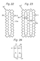
- Fig. 22 illustrates another embodiment of the multi-line minor loop pattern.
- This pattern 30' is a 2-line pattern similarto that in Fig. 21, in which two linear patterns 26 (-1, -2) are interconnected. In this case, however, the linear patterns 26 (-1, -2) are interconnected at their opposed ends, and the central portion 30A of the linear pattern 26-2 is cut off so as to define the full-length propagation path as mentioned hereinbefore. Otherwise, the linear pattern 26-1 may be partially cut off to define the full-length propagation path.
- Fig. 23 illustrates a further embodiment of the multi-line minor loop pattern.
- This pattern 30" is a 3-line pattern, in which three linear patterns 26 (-1, -2, -3) are interconnected, and the central portions 30B and 30C of the respective linear patterns 26-2 and 26-3 are cut off to define the full-length propagation path.
- the 3-line minor loop pattern 30" in arrangement of the cut-off portions of pattern, which will be generally described with reference to Fig. 24.
- three linear patterns are schematically illustrated with the references a 1 , a 2 and a3
- four connecting patterns are schematically illustrated with the references b l , b 2 , b 3 and b 4 .
- the first closed loop 1 1 can be opened by providing any one of four patterns a 1 , a 2 , b, and b 3 thereof with a cut-off portion
- the second closed loop 1 2 can be opened by providing any one of four patterns a 2 , a3, b 2 and b 4 thereof with a cut-off portion.
- Fig. 23 corresponds to one of these variations, in which the patterns a 2 and a3 are provided with the cut-off portions of pattern 30A and 30B.
- the multi-line patterns in which "n" linear patterns (n ⁇ 2) are interconnected, requires "n-1" cut-off portions of pattern to define the full-length propagation path.
- “n” is three or more, in particular, there are a number of variations in arrangement of the cut-off portion of pattern.
- the application of a pulse of current to the conductor pattern of the transfer gate causes the bubble to be transferred from the major loop pattern to the minor loop pattern, and vice versa.
- the pulse of transfer current is a square-shaped pulse and, accordingly, the bias field margins and the current margins are insufficient.
- Fig. 25 shows the bubble diameter versus bias field characteristics.
- the bubble In the magnetic field decreasing from the bias field H B , the bubble is striped out into the stripe domain at the elliptical instability field H so .
- the stripe domain In the magnetic field increasing towards the bias field H B , the stripe domain does not shrink in length until a field H sc , which is appreciably higher than the field H so , is reached.
- the operating characteristics of the transfer gate can be greatly improved by utilizing the above-mentioned transition hysteresis. This is attained by a feature that the pulse of transfer current applied to the conductor pattern to drive the transfer gate is a convex-shaped pulse.
- Fig. 26 illustrates a convex-shaped pulse which is composed of three parts, that is, a first base pulse P 1 , a summit pulse P 2 and an end base pulse P 3 .
- the first base pulse P 1 effects to expand the bubbles so as to make it easy to stripe out the bubbles
- the summit pulse P 2 effects to stripe out the expanded bubbles into the stripe domain
- the end base pulse P 3 effects to maintain the stripe domain constant in length until the position to which the bubble is to be transferred becomes attractive.
- ⁇ 1 , ⁇ 2 and ⁇ 3 designate the widths of the pulses P 1 , P 2 and P 3 , respectively, and I 1 designates the current of the summit pulse P 2 , and further 1 2 designates the currents of the base pulses P 2 and P 3 .
- the convex-shaped pulse mentioned above it is possible to make the width ⁇ 2 of the summit pulse P 2 narrower than that of the conventional square-shaped pulse. Consequently, the bias field margins and the current margins can be improved in contrast with those based on the conventional square-shaped pulse.
- Figs. 27 through 30 show the experimental data of the operating characteristics in the case wherein the above-mentioned convex-shaped pulse of current is applied to the transfer gate in Fig. 12.
- Fig. 27 shows the bias field margins depending on the summit pulse current I 1 at the constant base pulse current 1 2 of 50 mA.
- Fig. 28 shows the bias field margins depending on the base pulse current 1 2 at the constant summit pulse current I 1 of 100 mA. It will be understood from these figures that the best margins are obtained when the summit pulse current I 1 is 100 mA and the base pulse current 1 2 is 50 mA.
- Figs. 27 shows the bias field margins depending on the summit pulse current I 1 at the constant base pulse current 1 2 of 50 mA.
- the summit pulse width ⁇ 2 is constant to 0.3 ps
- the end base pulse width ⁇ 3 is constant to 0.2 ps
- the first base pulse width ⁇ 1 is varied to 0 ⁇ s, 0.15 ⁇ s and 0.3 ps.
- the summit pulse width ⁇ 2 is constant to 0.3 ⁇ s
- the first base pulse width ⁇ 1 is constant to 0.3 ps
- the end base pulse width ⁇ 3 is varied to 0 ps, 0.1 ⁇ s and 0.2 ⁇ s. It will be understood from these figures that the best bias field margins are obtained when the first base pulse width ⁇ 1 is 0.3 ⁇ s and the end base pulse width ⁇ 3 is 0.2 ps.
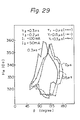
- Figs. 31 through 33 show comparatively the characteristics based on the convex-shaped pulse according to the present invention and the conventional square-shaped pulse.
- the graph A concerns the convex-shaped pulse, wherein the first base pulse width ⁇ 1 is 0.3 ⁇ s, the summit pulse width ⁇ 2 is 0.3 ps, and the end base pulse width ⁇ 3 is 0.2 ps.
- the graph B concerns the square-shaped pulse of 0.3 ⁇ s width
- the graph C concerns the square-shaped pulse of 0.8 ⁇ s width.
- Fig. 31 shows the bias field margins depending on the phase at the constant pulse current I (the summit. pulse current I 1 for the convex-shaped pulse) of 100 mA.
- Fig. 32 shows the current margins depending on the phase at the constant bias field margin H B of 330 Oe.
- Fig. 33 shows the bias field margins depending on the current at the constant phase 8 which is, of 110° for the convex-shaped pulse A, of 145° for the 0.3 pm width square-shaped pulse B, and of 110° for the 0.8 ⁇ m width square-shaped pulse C. It will be understood from these Figs. 31 through 33 that the convex-shaped pulse according to this aspect of the invention is superior to the square-shaped pulse.
- the present invention is applicable equally to cases in which the major loop pattern and the minor loop patterns are composed of disk patterns or square patterns.
Landscapes
- Thin Magnetic Films (AREA)
Claims (10)
Applications Claiming Priority (10)
| Application Number | Priority Date | Filing Date | Title |
|---|---|---|---|
| JP9734180A JPS5913105B2 (ja) | 1980-07-15 | 1980-07-15 | 連珠形デイスク・パタ−ン磁気バブル装置 |
| JP97341/80 | 1980-07-15 | ||
| JP2220781A JPS6037547B2 (ja) | 1981-02-19 | 1981-02-19 | イオン注入磁気バブルメモリ素子のゲ−ト駆動方法 |
| JP22207/81 | 1981-02-19 | ||
| JP2296081A JPS6037548B2 (ja) | 1981-02-20 | 1981-02-20 | 磁気バブルメモリ素子 |
| JP22960/81 | 1981-02-20 | ||
| JP56022959A JPS6059671B2 (ja) | 1981-02-20 | 1981-02-20 | 磁気バブルメモリ素子 |
| JP22961/81 | 1981-02-20 | ||
| JP22959/81 | 1981-02-20 | ||
| JP2296181A JPS6037549B2 (ja) | 1981-02-20 | 1981-02-20 | 磁気バブルメモリ素子 |
Publications (3)
| Publication Number | Publication Date |
|---|---|
| EP0044708A2 EP0044708A2 (de) | 1982-01-27 |
| EP0044708A3 EP0044708A3 (en) | 1984-03-28 |
| EP0044708B1 true EP0044708B1 (de) | 1987-06-24 |
Family
ID=27520425
Family Applications (1)
| Application Number | Title | Priority Date | Filing Date |
|---|---|---|---|
| EP81303260A Expired EP0044708B1 (de) | 1980-07-15 | 1981-07-15 | Magnetische Blasenspeicheranordnung |
Country Status (3)
| Country | Link |
|---|---|
| US (1) | US4415988A (de) |
| EP (1) | EP0044708B1 (de) |
| DE (1) | DE3176282D1 (de) |
Families Citing this family (5)
| Publication number | Priority date | Publication date | Assignee | Title |
|---|---|---|---|---|
| DE3365054D1 (en) * | 1982-02-22 | 1986-09-11 | Fujitsu Ltd | Ion-implanted magnetic bubble memory device |
| CA1197924A (en) * | 1982-06-23 | 1985-12-10 | Yoshio Satoh | Magnetic bubble memory device |
| FR2562706B1 (fr) * | 1984-04-05 | 1987-12-18 | Commissariat Energie Atomique | Duplicateur dans une memoire a bulles a motifs non implantes, procede pour la mise en oeuvre dudit duplicateur et memoire a bulles de type serie-parallele comportant au moins un desdits duplicateurs |
| FR2567300B1 (fr) * | 1984-07-09 | 1992-04-03 | Hitachi Ltd | Dispositif de memoire a bulles magnetiques |
| US4759020A (en) * | 1985-09-25 | 1988-07-19 | Unisys Corporation | Self-healing bubble memories |
Family Cites Families (6)
| Publication number | Priority date | Publication date | Assignee | Title |
|---|---|---|---|---|
| US4142250A (en) * | 1976-12-30 | 1979-02-27 | International Business Machines Corporation | Bubble translation switch using magnetic charged wall |
| US4176404A (en) * | 1978-01-13 | 1979-11-27 | Texas Instruments Incorporated | Bubble memory structure with enhanced data density |
| US4164027A (en) * | 1978-04-07 | 1979-08-07 | Control Data Corporation | Fault tolerant bubble memory with a single major loop having an integral stationary register |
| US4247912A (en) * | 1978-11-13 | 1981-01-27 | International Business Machines Corporation | Magnetic bubble domain chip with enhanced propagation margins |
| US4283776A (en) * | 1979-12-03 | 1981-08-11 | Bell Telephone Laboratories, Incorporated | Ion-implanted magnetic bubble memory |
| US4249249A (en) * | 1979-12-03 | 1981-02-03 | Bell Telephone Laboratories, Incorporated | Ion-implanted bubble memory |
-
1981
- 1981-07-14 US US06/283,182 patent/US4415988A/en not_active Expired - Fee Related
- 1981-07-15 DE DE8181303260T patent/DE3176282D1/de not_active Expired
- 1981-07-15 EP EP81303260A patent/EP0044708B1/de not_active Expired
Also Published As
| Publication number | Publication date |
|---|---|
| EP0044708A3 (en) | 1984-03-28 |
| DE3176282D1 (en) | 1987-07-30 |
| EP0044708A2 (de) | 1982-01-27 |
| US4415988A (en) | 1983-11-15 |
Similar Documents
| Publication | Publication Date | Title |
|---|---|---|
| US3523286A (en) | Magnetic single wall domain propagation device | |
| EP0044708B1 (de) | Magnetische Blasenspeicheranordnung | |
| Nelson et al. | Design of Bubble Device Elements Employing Ion‐Implanted Propagation Patterns | |
| US4079461A (en) | Gap tolerant bubble domain propagation circuits | |
| EP0011137A1 (de) | Herstellung eines Magnetblasendomänenchips mit verbesserten Propagationstoleranzen | |
| US3417385A (en) | Thin film shift register | |
| CA1130001A (en) | Contiguous element field access bubble lattice file | |
| EP0099750B1 (de) | Magnetische Blasenspeicheranordnung | |
| US3996572A (en) | Very high density gapless propagation structure for bubble domains | |
| EP0101187A2 (de) | Magnetische Blasenspeicheranordnung | |
| US4334291A (en) | Ion-implanted magnetic bubble memory with domain confinement rails | |
| EP0030149B1 (de) | Blasenspeicher mit Haupt-Nebenschleifen-Konfigurationen | |
| US4434476A (en) | Magnetic bubble memory device and method for operating the same | |
| CA1165874A (en) | Magnetic bubble memory | |
| US4012726A (en) | Magnetic bubble replicator | |
| Smith et al. | Dollar-sign transfer for magnetic bubbles | |
| US4387443A (en) | Magnetic bubble device | |
| US4357682A (en) | Conductorless transfer for magnetic bubble memories | |
| US4124901A (en) | Domain propagation register with single layer of conductors | |
| US4027297A (en) | Gapless magnetic bubble propagation path structure | |
| JPS592991B2 (ja) | 磁気バブルデバイスのマイナル−プ構成法 | |
| EP0087910B1 (de) | Ion-implantierter Magnetblasenspeicher | |
| CA1118097A (en) | Conductor access bubble memory | |
| US4698786A (en) | Magnetic bubble memory device | |
| US3641523A (en) | Magnetic domain circulating shift register |
Legal Events
| Date | Code | Title | Description |
|---|---|---|---|
| PUAI | Public reference made under article 153(3) epc to a published international application that has entered the european phase |
Free format text: ORIGINAL CODE: 0009012 |
|
| AK | Designated contracting states |
Designated state(s): DE FR GB NL |
|
| PUAL | Search report despatched |
Free format text: ORIGINAL CODE: 0009013 |
|
| AK | Designated contracting states |
Designated state(s): DE FR GB NL |
|
| 17P | Request for examination filed |
Effective date: 19840822 |
|
| GRAA | (expected) grant |
Free format text: ORIGINAL CODE: 0009210 |
|
| AK | Designated contracting states |
Kind code of ref document: B1 Designated state(s): DE FR GB NL |
|
| ET | Fr: translation filed | ||
| REF | Corresponds to: |
Ref document number: 3176282 Country of ref document: DE Date of ref document: 19870730 |
|
| PLBE | No opposition filed within time limit |
Free format text: ORIGINAL CODE: 0009261 |
|
| STAA | Information on the status of an ep patent application or granted ep patent |
Free format text: STATUS: NO OPPOSITION FILED WITHIN TIME LIMIT |
|
| 26N | No opposition filed | ||
| PGFP | Annual fee paid to national office [announced via postgrant information from national office to epo] |
Ref country code: GB Payment date: 19920630 Year of fee payment: 12 |
|
| PGFP | Annual fee paid to national office [announced via postgrant information from national office to epo] |
Ref country code: FR Payment date: 19920730 Year of fee payment: 12 |
|
| PGFP | Annual fee paid to national office [announced via postgrant information from national office to epo] |
Ref country code: NL Payment date: 19920731 Year of fee payment: 12 |
|
| PGFP | Annual fee paid to national office [announced via postgrant information from national office to epo] |
Ref country code: DE Payment date: 19920922 Year of fee payment: 12 |
|
| PG25 | Lapsed in a contracting state [announced via postgrant information from national office to epo] |
Ref country code: GB Effective date: 19930715 |
|
| PG25 | Lapsed in a contracting state [announced via postgrant information from national office to epo] |
Ref country code: NL Effective date: 19940201 |
|
| GBPC | Gb: european patent ceased through non-payment of renewal fee |
Effective date: 19930715 |
|
| NLV4 | Nl: lapsed or anulled due to non-payment of the annual fee | ||
| PG25 | Lapsed in a contracting state [announced via postgrant information from national office to epo] |
Ref country code: FR Effective date: 19940331 |
|
| PG25 | Lapsed in a contracting state [announced via postgrant information from national office to epo] |
Ref country code: DE Effective date: 19940401 |
|
| REG | Reference to a national code |
Ref country code: FR Ref legal event code: ST |