EP0046501B1 - Verfahren zum Herstellen dielektrischer Bereiche, die in einem Siliziumsubstrat eingelassen sind - Google Patents
Verfahren zum Herstellen dielektrischer Bereiche, die in einem Siliziumsubstrat eingelassen sind Download PDFInfo
- Publication number
- EP0046501B1 EP0046501B1 EP81105496A EP81105496A EP0046501B1 EP 0046501 B1 EP0046501 B1 EP 0046501B1 EP 81105496 A EP81105496 A EP 81105496A EP 81105496 A EP81105496 A EP 81105496A EP 0046501 B1 EP0046501 B1 EP 0046501B1
- Authority
- EP
- European Patent Office
- Prior art keywords
- layer
- substrate
- polycrystalline silicon
- silicon
- dielectric material
- Prior art date
- Legal status (The legal status is an assumption and is not a legal conclusion. Google has not performed a legal analysis and makes no representation as to the accuracy of the status listed.)
- Expired
Links
Images
Classifications
-
- G—PHYSICS
- G03—PHOTOGRAPHY; CINEMATOGRAPHY; ANALOGOUS TECHNIQUES USING WAVES OTHER THAN OPTICAL WAVES; ELECTROGRAPHY; HOLOGRAPHY
- G03F—PHOTOMECHANICAL PRODUCTION OF TEXTURED OR PATTERNED SURFACES, e.g. FOR PRINTING, FOR PROCESSING OF SEMICONDUCTOR DEVICES; MATERIALS THEREFOR; ORIGINALS THEREFOR; APPARATUS SPECIALLY ADAPTED THEREFOR
- G03F7/00—Photomechanical, e.g. photolithographic, production of textured or patterned surfaces, e.g. printing surfaces; Materials therefor, e.g. comprising photoresists; Apparatus specially adapted therefor
- G03F7/004—Photosensitive materials
- G03F7/09—Photosensitive materials characterised by structural details, e.g. supports, auxiliary layers
- G03F7/094—Multilayer resist systems, e.g. planarising layers
-
- H—ELECTRICITY
- H10—SEMICONDUCTOR DEVICES; ELECTRIC SOLID-STATE DEVICES NOT OTHERWISE PROVIDED FOR
- H10P—GENERIC PROCESSES OR APPARATUS FOR THE MANUFACTURE OR TREATMENT OF DEVICES COVERED BY CLASS H10
- H10P50/00—Etching of wafers, substrates or parts of devices
- H10P50/20—Dry etching; Plasma etching; Reactive-ion etching
- H10P50/26—Dry etching; Plasma etching; Reactive-ion etching of conductive or resistive materials
- H10P50/264—Dry etching; Plasma etching; Reactive-ion etching of conductive or resistive materials by chemical means
- H10P50/266—Dry etching; Plasma etching; Reactive-ion etching of conductive or resistive materials by chemical means by vapour etching only
- H10P50/267—Dry etching; Plasma etching; Reactive-ion etching of conductive or resistive materials by chemical means by vapour etching only using plasmas
- H10P50/268—Dry etching; Plasma etching; Reactive-ion etching of conductive or resistive materials by chemical means by vapour etching only using plasmas of silicon-containing layers
-
- H—ELECTRICITY
- H10—SEMICONDUCTOR DEVICES; ELECTRIC SOLID-STATE DEVICES NOT OTHERWISE PROVIDED FOR
- H10P—GENERIC PROCESSES OR APPARATUS FOR THE MANUFACTURE OR TREATMENT OF DEVICES COVERED BY CLASS H10
- H10P50/00—Etching of wafers, substrates or parts of devices
- H10P50/20—Dry etching; Plasma etching; Reactive-ion etching
- H10P50/28—Dry etching; Plasma etching; Reactive-ion etching of insulating materials
- H10P50/282—Dry etching; Plasma etching; Reactive-ion etching of insulating materials of inorganic materials
- H10P50/283—Dry etching; Plasma etching; Reactive-ion etching of insulating materials of inorganic materials by chemical means
-
- H—ELECTRICITY
- H10—SEMICONDUCTOR DEVICES; ELECTRIC SOLID-STATE DEVICES NOT OTHERWISE PROVIDED FOR
- H10P—GENERIC PROCESSES OR APPARATUS FOR THE MANUFACTURE OR TREATMENT OF DEVICES COVERED BY CLASS H10
- H10P50/00—Etching of wafers, substrates or parts of devices
- H10P50/20—Dry etching; Plasma etching; Reactive-ion etching
- H10P50/28—Dry etching; Plasma etching; Reactive-ion etching of insulating materials
- H10P50/286—Dry etching; Plasma etching; Reactive-ion etching of insulating materials of organic materials
- H10P50/287—Dry etching; Plasma etching; Reactive-ion etching of insulating materials of organic materials by chemical means
-
- H—ELECTRICITY
- H10—SEMICONDUCTOR DEVICES; ELECTRIC SOLID-STATE DEVICES NOT OTHERWISE PROVIDED FOR
- H10P—GENERIC PROCESSES OR APPARATUS FOR THE MANUFACTURE OR TREATMENT OF DEVICES COVERED BY CLASS H10
- H10P50/00—Etching of wafers, substrates or parts of devices
- H10P50/60—Wet etching
- H10P50/66—Wet etching of conductive or resistive materials
- H10P50/663—Wet etching of conductive or resistive materials by chemical means only
- H10P50/667—Wet etching of conductive or resistive materials by chemical means only by liquid etching only
-
- H—ELECTRICITY
- H10—SEMICONDUCTOR DEVICES; ELECTRIC SOLID-STATE DEVICES NOT OTHERWISE PROVIDED FOR
- H10P—GENERIC PROCESSES OR APPARATUS FOR THE MANUFACTURE OR TREATMENT OF DEVICES COVERED BY CLASS H10
- H10P95/00—Generic processes or apparatus for manufacture or treatments not covered by the other groups of this subclass
- H10P95/06—Planarisation of inorganic insulating materials
- H10P95/062—Planarisation of inorganic insulating materials involving a dielectric removal step
- H10P95/064—Planarisation of inorganic insulating materials involving a dielectric removal step the removal being chemical etching
-
- H—ELECTRICITY
- H10—SEMICONDUCTOR DEVICES; ELECTRIC SOLID-STATE DEVICES NOT OTHERWISE PROVIDED FOR
- H10W—GENERIC PACKAGES, INTERCONNECTIONS, CONNECTORS OR OTHER CONSTRUCTIONAL DETAILS OF DEVICES COVERED BY CLASS H10
- H10W10/00—Isolation regions in semiconductor bodies between components of integrated devices
- H10W10/01—Manufacture or treatment
- H10W10/011—Manufacture or treatment of isolation regions comprising dielectric materials
- H10W10/014—Manufacture or treatment of isolation regions comprising dielectric materials using trench refilling with dielectric materials, e.g. shallow trench isolations
- H10W10/0145—Manufacture or treatment of isolation regions comprising dielectric materials using trench refilling with dielectric materials, e.g. shallow trench isolations of trenches having shapes other than rectangular or V-shape
-
- H—ELECTRICITY
- H10—SEMICONDUCTOR DEVICES; ELECTRIC SOLID-STATE DEVICES NOT OTHERWISE PROVIDED FOR
- H10W—GENERIC PACKAGES, INTERCONNECTIONS, CONNECTORS OR OTHER CONSTRUCTIONAL DETAILS OF DEVICES COVERED BY CLASS H10
- H10W10/00—Isolation regions in semiconductor bodies between components of integrated devices
- H10W10/10—Isolation regions comprising dielectric materials
- H10W10/17—Isolation regions comprising dielectric materials formed using trench refilling with dielectric materials, e.g. shallow trench isolations
Definitions
- the present invention relates to an improved method for fabricating a semiconductor device provided with recessed regions of dielectric material for isolating individual elements of the device, more particularly to a method of forming deep dielectric isolation zones or regions wherein the improvement is restoring surface planarity to the substrate during the removal of excess dielectric material used to form the dielectric regions.
- dielectric isolation in integrated circuit devices has a substantial advantage over the PN junction isolation because potentially it allows the butting of the circuit elements against the isolation regions and thereby achieves greater density of packing of the active and passive devices on the integrated circuit device.
- One form of dielectric isolation involves the formation of grooves or depressions in silicon where the isolation regions are to be formed. During the groove formation the remainder of the silicon surface is protected by a protective film which is substantially unaffected by the silicon etch used to form the grooves and also to an oxidative environment.
- the usual protective layer is a silicon nitrile/silicon dioxide sandwich layer.
- the silicon body is subjected to a conventional oxidation step whereby the silicon in the groove area is oxidized and the silicon dioxide fills up the groove as well as oxidizing further into the silicon to form the isolation region.
- One of the major problems with this process is what is known as "bird's beak".
- the "bird's beak” is a nonplanar silicon dioxide formation at the top periphery of the groove and is caused by the lateral oxidation underneath the silicon nitride layer. Since the oxidation of a specific thickness of silicon requires an almost equivalent amount of free space to expand into, and since the Si 3 N 4 limits the unrestricted expansion, the result is an up- pushing of the silicon nitride at the edge of the groove. The final consequence of this is a general stress in the perimeter region of the groove as well as difficulties in subsequently achieving good butted diffusions against the vertical portion of the silicon dioxide. This non- butting capability defeats a major benefit of the original purpose of the silicon dioxide region. This process is described more fully by E. Kooi U.S. Pat. No. 3 970 486, Clevenger U.S. Pat. No. 3 534 234, Peltzer U.S. Pat. No. 3 648 125.
- the openings are then filled by vapor deposition of polycrystalline silicon, silicon dioxide, or similar materials.
- This technique has some disadvantages. Selective epitaxy, as required by this technique, is very sensitive to the area relationship between silicon dioxide and silicon regions. For example, two different size silicon regions would tend to fill in at a different rate so that at the end of a process the regions are filled in to a different extent. Also, in messa-type depositions, crystallographic faceting tends to occur. This results in pyramid-like growth and tends to widen the isolation regions beyond the original lithography capabilities. The slanted silicon/silicon dioxide interface will again cause difficulties in achieving reliable butted diffusions against the silicon dioxide region.
- U.S. Pat. No. 4 073 054 describes a method for forming a region of an electrical insulator between elements of a semiconductor integrated circuit device.
- a semiconductor substrate is covered with a first electrical insulator and a groove provided in the substrate. This groove is filled with insulating material, then the device is coated with a second electrical insulator which is etched subsequently at a rate approximately equivalent to that of the first insulator. Then, both insulator layers are removed until the surface of the substrate is exposed.
- U.S. Pat. No. 4 106 086 discloses a process for forming deep recessed oxide isolation regions in a silicon substrate wherein grooves are formed in the substrate using reactive ion etching, a layer of Si0 2 formed on the surface to fill the grooves, and the Si0 2 layer subsequently removed everywhere on the surface except where the material is disposed in the grooves.
- a shortcoming of this process is that the thickness of the Si0 2 layer is not always uniform, and the surface is not planar. Thickness variations in a deposited layer, particularly a relatively thick layer are common, and the top surface of a chemical vapor deposited layer that has been deposited over a non-planar surface is also not planar. Cusps are commonly formed over the grooves.
- top Si0 2 layer with a non-uniform thickness and a non-planar surface is removed by reactive ion etching, portions of the silicon substrate where the oxide layer is thinner might also be removed. If thin diffused regions are in the substrate, a substrate might be rendered useless. Further, the non-planarity of the top surface of the silicon oxide layer is propulgated down to the resultant semiconductor surface. Such unevenness of the surface of the semiconductor device which will be fabricated into an integrated circuit device, disrupts the fabrication of the masking and associated process steps necessary for forming the device as well as causing difficulty in fabricating the various metallurgy stripes on the surface.
- this invention intends to provide an improved process for forming deep dielectric isolation regions in which the silicon substrate is protected during etch-back of the dielectric layer used for form isolation regions and, also, to provide a process for producing recessed dielectric regions that include the step of planarizing the resultant substrate.
- the present invention as claimed provides a solution for these problems.
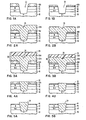
- Figs. 1 A-B through Figs. 5A-B depict a sequence of cross-sectional views which illustrate the process of the invention and the inherent thickness variations of depositing films.
- FIGs. 1 A-B through Figs. 5A-B the manufacturing steps for forming recessed oxide region in a semiconductor device are illustrated.
- the vertical dimensions in the figures are exaggerated to more clearly illustrate the problems of the art.
- a and B are cross-sectional views taken at different locations on a semiconductor wafer or on different wafers in a batch of wafers undergoing the same process steps. Different cross-sectional views are illustrated to show the effects of inherent process variations on the product and better explain the invention for compensating for such variables.
- the sequence of Figs. 1 A through 5A show views where the accumulated variations results in a deposition of thicker film than the average thickness of the film.
- FIG. 1A and Fig. 1B show accumulated variations where the deposition of the films are thinner than the average thickness of the films.
- the structure illustrated in Fig. 1A and Fig. 1B includes a monocrystalline silicon substrate 10, which is shown as P- conductivity for illustration purposes, with an N+ layer 12 over substrate 10 and an N- conductivity layer 14 on layer 12.
- a monocrystalline silicon substrate 10 which is shown as P- conductivity for illustration purposes, with an N+ layer 12 over substrate 10 and an N- conductivity layer 14 on layer 12.
- the layer 12 be a high conductivity region where it will ultimately be the collector of a bi-polar transistor.
- This structure can be fabricated by various techniques.
- the preferred technique is to provide a P- monocrystalline silicon substrate and diffuse an N+ blanket diffusion into the substrate by using conventional diffusion or ion implantation of an N type impurity such as arsenic antimony or phosphorus to produce the N+ region with a surface concentration of between 1 ⁇ 10 19 and 1 ⁇ 10 21 atoms per cm 3 .
- the layer 14 is subsequently grown onto substrate 10 over layer 12 by means of epitaxial growth. This may be done by conventional techniques such as the use of SiCl 4 /H 2 or SiH 4 /H 2 mixtures at growth temperatures of about 1000°C to 1200°C.
- the N+ layer may have a typical thickness of between 1 to 3 pm, whereas the epitaxial layer has a thickness of 0.5 to 10 11 m, the exact thickness depending upon the device to be built.
- the structure could be made by various combinations of thermal diffusions ion implantations and/or epitaxial growth which would include the formation of a buried subcollector region where the subsequent formation of bi-polar devices is desired.
- a silicon dioxide layer 16 is formed by conventional techniques of either thermal growth in a wet or dry oxygen ambient or by chemical vapor deposition. The thickness of layer 16 can be any suitable thickness typically between 250 to 10000 A, more preferably 1000 to 3000 A.
- a layer of polysilicon 18 is deposited over Si0 2 layer 16 using conventional techniques.
- the polysilicon layer 18 can be deposited with the same apparatus used to form epitaxial layer 14, described previously or by any conventional deposition technique.
- the thickness of the polysilicon layer must be sufficient to compensate for any accumulation of deposition and etchant removal techniques used in the process which follows. The description of applicants' process which follows will provide a more clear understanding. In general the thickness of layer 18 will be in the range of 0.2 to 1.5 ⁇ m for typical device application.
- trenches or grooves 20 In order to form recessed oxide regions in a device, trenches or grooves 20 must be formed to a depth sufficient to reach through N+ region 12. These grooves 20 can be formed by any suitable technique, but are preferably formed by reactive ion etching. Techniques for forming grooves in a semiconductor by reactive ion etching techniques are described in Hochberg U.S. Pat. No. 3 966 577 and T. Kaji et al U.S. Pat. No. 3 997 378, and S. A. Abbas, IBM TDB Vol. 20, No. 1, P. 144 June 1977 entitled "Recessed Oxide Isolation Process".
- a suitable mask is formed on the top surface of polysilicon layer 18A and 18B and the substrate exposed to reactive ion etching.
- a typical technique for forming a mask is to oxidize the surface of polysilicon layer 18A and 18B and remove portions thereof by conventional photolithographic techniques overlying the areas where trenches are desired. The masking layer is not illustrated since it is conventional in the art.
- Trenches 20 are then formed resulting in the cross-section shown in Figs. 1A and 1B. The depth of the trenches must be sufficient to extent beneath N+ diffused region 12 in both Fig. 1 A having a thicker layer 18A as well as Fig. B with a thinner layer 18B. In addition, there are inherent variations in the depth of the trench 20 using the surfaces of layer 18A and 18B as a reference.
- the next step in the process of forming recessed oxide regions is filling the grooves 20 with a suitable dielectric material.
- a blanket layer 22A and 22B of dielectric material must have a thickness at least one-half the width of the groove 20 or equal to the depth of the groove 20, whichever is appropriate.
- a preferred dielectric material for filling groove 20 is Si0 2 deposited by a chemical vapor deposition techniques using gas mixtures of CO 2 /SiH 4 /N 2 or N 2 O/SiH 4 /N 2 at 800-1000-C.
- Typical deposition rates are of the order of 50 to 200 A per minute and the total deposition thickness is at least one-half the width of groove 20.
- the width of groove 20 varies typically from 0.1 ⁇ m to 500 ⁇ m and the depth of groove 20 varies typically from 0.2 pm to 10 ⁇ m.
- the thickness of Si0 2 layer 22A and 22B also will inherently vary at different locations on the wafer, and from wafer to wafer by a figure of 10%. This, again, is illustrated in Figs. 2A and 2B wherein the layer 22A is thicker than layer 22B in Fig. 2B.
- Another approach, not illustrated, in filling grooves 20 with dielectric material is to initially form a thin layer of thermal oxide on the sidewalls of the trench 20.
- a thermal oxide layer can conveniently be formed by subjecting the substrates to an oxidation ambient which may be, for example, 970°C in wet oxygen.
- the substrate is subjected to the ambient for 10 to 30 minutes to produce a Si0 2 thickness within the trench 20 of about 500 to 200 A.
- the chemically vapor- deposited layer 22A and 22B can then be formed over the top surface of the thermal oxide layer in the groove.
- a depression or cusp 24 is formed on the surface over the filled channel 20. If a uniform surface thickness is removed from layer 22, the depression 24 will be propulgated downwardly and appear in the surface of the device. The depression can cause probelms in fabricating the necessary metallurgy on the finished device.
- a layer 26 of material is flowed over the surface to fill in the depression 24 to achieve a relatively planar surface 28.
- Layer 26 is preferably a layer of organic material such as polyimide resin, or a suitable resist material.
- the thickness can be any suitable thickness, preferably from 1 to 3.0 ⁇ m. As indicated in Figs. 3A and 3B, variations in the thickness can result in the layer 26. In Fig. 3A the layer 26A is indicated as thicker than layer 26B in Fig. 3B.
- layer 26, 22, and a portion of 18 are removed leaving the trench 20 filled with dielectric material which will serve as isolation regions encircling monocrystalline device regions to provide electrical isolation between associated elements on the same substrate.
- This removal step is accomplished by reactive ion etching of layer 26, layer 22 and a portion of layer 18.
- the system used for this process is preferably a low pressure sputter etch system with the substrate positioned on a silicon cathode cover plate.
- a fluorinated hydrocarbon such as CF 4 is used as an etchant so that the organic material/SiO 2 /Si etch rate ratio of approximately 1 to 1 to 1 results.
- the gas pressure could run from 10 to 70 I tm Hg with gas flow rates of 2 to 50 cm 3 /min.
- the RF power level is preferably from 0.2 watts/cm 2 to 0.5 watts/cm 2 .
- the reactive ion etching operation thus starts with a relatively smooth surface 28 and maintains this surface as the layers are progressively etched away, since the etch rates of Si, Si0 2 and polyimide are approximately the same.
- the objective of the removal process is to maintain a relatively planar surface while removing the materials above layer 16. Since the total thickness of the layers above layer 16 can vary due to inherent process variations, removal of the layers down to layer 16 at some locations where the layers were the thinnest would remove significant parts of layer 16 and region 14 which is unacceptable.
- the final step in forming the recessed regions by the method of our invention is removal of the remaining polysilicon material of layer 18 as shown in Figs. 5A and 5B.
- an etchant that selectively etches only the polysilicon and not the silicon dioxide material.
- Such an etch is pyrocatechol.
- the pyrocatechol etchant will remove all of the polysilicon above the Si0 2 layer 16 in both the cross-sectional views shown in Figs.
- the layer 16 serves as an etchant stop. Extreme care must be taken not to remove layer 16 or to allow the oxide refill to etch below layer 16* during the reactive ion etching process, otherwise the etchant for polysilicon layer 18 will attack the underlying silicon in region 14 and destroy the device. Alternately, the remaining polysilicon material can be removed by reactive ion etching in an ambient that selectively removes silicon. Examples are: SF with a polysilicon-to-oxide etchant ratio of 15:1 or SF 6 /Cl with a polysilicon-to-oxide.
- Fig. 5A there is a slight protrusion of recessed oxide region 34 above the surface of layer 16. However, the top surface of region 34 is planar without the depression 24 present in the deposited layer 22.
- the device shown in Figs. 5A and 5B can then be further processed by forming diffusion openings in layer 16 and making the necessary diffusions to form the desired device structure. Subsequently, metallurgy can be deposited as is conventional in the art to form very dense integrated circuit devices.
Landscapes
- Engineering & Computer Science (AREA)
- Architecture (AREA)
- Structural Engineering (AREA)
- Physics & Mathematics (AREA)
- General Physics & Mathematics (AREA)
- Element Separation (AREA)
- Local Oxidation Of Silicon (AREA)
- Drying Of Semiconductors (AREA)
Claims (9)
Applications Claiming Priority (2)
| Application Number | Priority Date | Filing Date | Title |
|---|---|---|---|
| US06/180,535 US4307180A (en) | 1980-08-22 | 1980-08-22 | Process of forming recessed dielectric regions in a monocrystalline silicon substrate |
| US180535 | 1980-08-22 |
Publications (2)
| Publication Number | Publication Date |
|---|---|
| EP0046501A1 EP0046501A1 (de) | 1982-03-03 |
| EP0046501B1 true EP0046501B1 (de) | 1984-10-31 |
Family
ID=22660805
Family Applications (1)
| Application Number | Title | Priority Date | Filing Date |
|---|---|---|---|
| EP81105496A Expired EP0046501B1 (de) | 1980-08-22 | 1981-07-14 | Verfahren zum Herstellen dielektrischer Bereiche, die in einem Siliziumsubstrat eingelassen sind |
Country Status (5)
| Country | Link |
|---|---|
| US (1) | US4307180A (de) |
| EP (1) | EP0046501B1 (de) |
| JP (1) | JPS5763843A (de) |
| CA (1) | CA1159966A (de) |
| DE (1) | DE3166951D1 (de) |
Families Citing this family (43)
| Publication number | Priority date | Publication date | Assignee | Title |
|---|---|---|---|---|
| US4394196A (en) * | 1980-07-16 | 1983-07-19 | Tokyo Shibaura Denki Kabushiki Kaisha | Method of etching, refilling and etching dielectric grooves for isolating micron size device regions |
| US4374011A (en) * | 1981-05-08 | 1983-02-15 | Fairchild Camera & Instrument Corp. | Process for fabricating non-encroaching planar insulating regions in integrated circuit structures |
| US4493740A (en) * | 1981-06-01 | 1985-01-15 | Matsushita Electric Industrial Company, Limited | Method for formation of isolation oxide regions in semiconductor substrates |
| JPS57204133A (en) * | 1981-06-10 | 1982-12-14 | Hitachi Ltd | Manufacture of semiconductor integrated circuit |
| US4389294A (en) * | 1981-06-30 | 1983-06-21 | International Business Machines Corporation | Method for avoiding residue on a vertical walled mesa |
| JPS5873163A (ja) * | 1981-10-27 | 1983-05-02 | Toshiba Corp | Mos型半導体装置 |
| FR2529714A1 (fr) * | 1982-07-01 | 1984-01-06 | Commissariat Energie Atomique | Procede de realisation de l'oxyde de champ d'un circuit integre |
| US4508757A (en) * | 1982-12-20 | 1985-04-02 | International Business Machines Corporation | Method of manufacturing a minimum bird's beak recessed oxide isolation structure |
| JPS59215741A (ja) * | 1983-05-24 | 1984-12-05 | Mitsubishi Electric Corp | 半導体集積回路装置の製造方法 |
| JPS59225543A (ja) * | 1983-06-06 | 1984-12-18 | Mitsubishi Electric Corp | 素子間分離領域の形成方法 |
| JPH0642510B2 (ja) * | 1983-06-13 | 1994-06-01 | エヌ・シー・アール・インターナショナル・インコーポレイテッド | 半導体構造の形成方法 |
| US4604162A (en) * | 1983-06-13 | 1986-08-05 | Ncr Corporation | Formation and planarization of silicon-on-insulator structures |
| JPS6054450A (ja) * | 1983-09-05 | 1985-03-28 | Oki Electric Ind Co Ltd | 半導体装置の製造方法 |
| JPS60115234A (ja) * | 1983-11-28 | 1985-06-21 | Toshiba Corp | 半導体装置の製造方法 |
| US4534824A (en) * | 1984-04-16 | 1985-08-13 | Advanced Micro Devices, Inc. | Process for forming isolation slots having immunity to surface inversion |
| JPS60245249A (ja) * | 1984-05-21 | 1985-12-05 | Nec Corp | 素子分離領域の形成方法 |
| JPS618945A (ja) * | 1984-06-25 | 1986-01-16 | Nec Corp | 半導体集積回路装置 |
| JPS6161431A (ja) * | 1984-09-03 | 1986-03-29 | Nec Corp | 半導体装置の製造方法 |
| US4541169A (en) * | 1984-10-29 | 1985-09-17 | International Business Machines Corporation | Method for making studs for interconnecting metallization layers at different levels in a semiconductor chip |
| US4541168A (en) * | 1984-10-29 | 1985-09-17 | International Business Machines Corporation | Method for making metal contact studs between first level metal and regions of a semiconductor device compatible with polyimide-filled deep trench isolation schemes |
| US4571819A (en) * | 1984-11-01 | 1986-02-25 | Ncr Corporation | Method for forming trench isolation structures |
| US4665010A (en) * | 1985-04-29 | 1987-05-12 | International Business Machines Corporation | Method of fabricating photopolymer isolation trenches in the surface of a semiconductor wafer |
| US4662064A (en) * | 1985-08-05 | 1987-05-05 | Rca Corporation | Method of forming multi-level metallization |
| US4671851A (en) * | 1985-10-28 | 1987-06-09 | International Business Machines Corporation | Method for removing protuberances at the surface of a semiconductor wafer using a chem-mech polishing technique |
| US4791073A (en) * | 1987-11-17 | 1988-12-13 | Motorola Inc. | Trench isolation method for semiconductor devices |
| US4851370A (en) * | 1987-12-28 | 1989-07-25 | American Telephone And Telegraph Company, At&T Bell Laboratories | Fabricating a semiconductor device with low defect density oxide |
| DE354669T1 (de) * | 1988-07-20 | 1990-11-08 | Hashimoto Chemical Industries Co., Ltd., Sakai, Osaka | Einrichtung und verfahren zum trockenaetzen und generator zum erzeugen von wasserfreier, verduennter fluss-saeure, die dafuer benoetigt wird. |
| US4973544A (en) * | 1989-03-07 | 1990-11-27 | Hughes Aircraft Company | Method for reversing tone or polarity of pattern on integrated circuit substrate utilizing reverse casting by planarization |
| US5159429A (en) * | 1990-01-23 | 1992-10-27 | International Business Machines Corporation | Semiconductor device structure employing a multi-level epitaxial structure and method of manufacturing same |
| US4997775A (en) * | 1990-02-26 | 1991-03-05 | Cook Robert K | Method for forming a complementary bipolar transistor structure including a self-aligned vertical PNP transistor |
| US5480832A (en) * | 1991-10-14 | 1996-01-02 | Nippondenso Co., Ltd. | Method for fabrication of semiconductor device |
| DE4202651A1 (de) * | 1992-01-30 | 1993-08-05 | Fraunhofer Ges Forschung | Verfahren zur trockenentwicklung einer siliziumhaltigen ultraviolett- und/oder elektronenstrahlempfindlichen lackschicht |
| US5229316A (en) * | 1992-04-16 | 1993-07-20 | Micron Technology, Inc. | Semiconductor processing method for forming substrate isolation trenches |
| US5395789A (en) * | 1993-08-06 | 1995-03-07 | At&T Corp. | Integrated circuit with self-aligned isolation |
| US6322634B1 (en) * | 1997-01-27 | 2001-11-27 | Micron Technology, Inc. | Shallow trench isolation structure without corner exposure |
| US5981354A (en) * | 1997-03-12 | 1999-11-09 | Advanced Micro Devices, Inc. | Semiconductor fabrication employing a flowable oxide to enhance planarization in a shallow trench isolation process |
| JP3904676B2 (ja) * | 1997-04-11 | 2007-04-11 | 株式会社ルネサステクノロジ | トレンチ型素子分離構造の製造方法およびトレンチ型素子分離構造 |
| TW395024B (en) * | 1998-08-28 | 2000-06-21 | United Microelectronics Corp | The method to shape up a shallow trench for isolation in IC |
| KR100674896B1 (ko) * | 2000-07-26 | 2007-01-26 | 삼성전자주식회사 | 반도체 집적회로의 트렌치 소자 분리 방법 |
| US7060573B2 (en) * | 2001-01-16 | 2006-06-13 | Chartered Semiconductor Manufacturing Ltd. | Extended poly buffer STI scheme |
| US6730609B2 (en) * | 2001-10-09 | 2004-05-04 | Micron Technology, Inc. | Etch aided by electrically shorting upper and lower sidewall portions during the formation of a semiconductor device |
| US7141478B2 (en) * | 2004-01-26 | 2006-11-28 | Legerity Inc. | Multi-stage EPI process for forming semiconductor devices, and resulting device |
| CN102479738B (zh) * | 2010-11-23 | 2014-05-28 | 中国科学院微电子研究所 | 沟槽隔离结构及其形成方法 |
Family Cites Families (7)
| Publication number | Priority date | Publication date | Assignee | Title |
|---|---|---|---|---|
| DE2547792C3 (de) * | 1974-10-25 | 1978-08-31 | Hitachi, Ltd., Tokio | Verfahren zur Herstellung eines Halbleiterbauelementes |
| JPS5226182A (en) * | 1975-08-25 | 1977-02-26 | Hitachi Ltd | Manufacturing method of semi-conductor unit |
| US4104090A (en) * | 1977-02-24 | 1978-08-01 | International Business Machines Corporation | Total dielectric isolation utilizing a combination of reactive ion etching, anodic etching, and thermal oxidation |
| JPS54589A (en) * | 1977-06-03 | 1979-01-05 | Hitachi Ltd | Burying method of insulator |
| US4104086A (en) * | 1977-08-15 | 1978-08-01 | International Business Machines Corporation | Method for forming isolated regions of silicon utilizing reactive ion etching |
| EP0023146B1 (de) * | 1979-07-23 | 1987-09-30 | Fujitsu Limited | Verfahren zur Herstellung einer Halbleiteranordnung, in der erste und zweite Schichten geformt sind |
| US4222792A (en) * | 1979-09-10 | 1980-09-16 | International Business Machines Corporation | Planar deep oxide isolation process utilizing resin glass and E-beam exposure |
-
1980
- 1980-08-22 US US06/180,535 patent/US4307180A/en not_active Expired - Lifetime
-
1981
- 1981-06-19 JP JP56094093A patent/JPS5763843A/ja active Pending
- 1981-07-07 CA CA000381235A patent/CA1159966A/en not_active Expired
- 1981-07-14 EP EP81105496A patent/EP0046501B1/de not_active Expired
- 1981-07-14 DE DE8181105496T patent/DE3166951D1/de not_active Expired
Also Published As
| Publication number | Publication date |
|---|---|
| DE3166951D1 (en) | 1984-12-06 |
| EP0046501A1 (de) | 1982-03-03 |
| US4307180A (en) | 1981-12-22 |
| CA1159966A (en) | 1984-01-03 |
| JPS5763843A (en) | 1982-04-17 |
Similar Documents
| Publication | Publication Date | Title |
|---|---|---|
| EP0046501B1 (de) | Verfahren zum Herstellen dielektrischer Bereiche, die in einem Siliziumsubstrat eingelassen sind | |
| US4104086A (en) | Method for forming isolated regions of silicon utilizing reactive ion etching | |
| EP0036111B1 (de) | Verfahren zur Herstellung einer feinen, tiefen dielektrischen Isolation | |
| US4502913A (en) | Total dielectric isolation for integrated circuits | |
| KR100213196B1 (ko) | 트렌치 소자분리 | |
| US5445989A (en) | Method of forming device isolation regions | |
| US4222792A (en) | Planar deep oxide isolation process utilizing resin glass and E-beam exposure | |
| US4755477A (en) | Overhang isolation technology | |
| US4271583A (en) | Fabrication of semiconductor devices having planar recessed oxide isolation region | |
| KR100224700B1 (ko) | 반도체장치의 소자분리방법 | |
| US5294562A (en) | Trench isolation with global planarization using flood exposure | |
| US4661832A (en) | Total dielectric isolation for integrated circuits | |
| US5565376A (en) | Device isolation technology by liquid phase deposition | |
| US4900689A (en) | Method of fabrication of isolated islands for complementary bipolar devices | |
| US4389294A (en) | Method for avoiding residue on a vertical walled mesa | |
| CA2015891C (en) | Method for forming variable width isolation structures | |
| US5234861A (en) | Method for forming variable width isolation structures | |
| KR0172792B1 (ko) | 반도체소자의 소자분리 영역의 제조방법 | |
| KR0185479B1 (ko) | 반도체 소자의 소자분리막 형성방법 | |
| US5851901A (en) | Method of manufacturing an isolation region of a semiconductor device with advanced planarization | |
| US6627492B2 (en) | Methods of forming polished material and methods of forming isolation regions | |
| KR100195237B1 (ko) | 개선된 트렌치와 로코스 조합형 소자분리방법 | |
| JPS58200554A (ja) | 半導体装置の製造方法 | |
| KR100954418B1 (ko) | 반도체 소자의 소자분리막 형성방법 | |
| CA1108772A (en) | Method for forming isolated regions of silicon |
Legal Events
| Date | Code | Title | Description |
|---|---|---|---|
| PUAI | Public reference made under article 153(3) epc to a published international application that has entered the european phase |
Free format text: ORIGINAL CODE: 0009012 |
|
| 17P | Request for examination filed |
Effective date: 19811029 |
|
| AK | Designated contracting states |
Designated state(s): DE FR GB IT |
|
| GRAA | (expected) grant |
Free format text: ORIGINAL CODE: 0009210 |
|
| AK | Designated contracting states |
Designated state(s): DE FR GB IT |
|
| PG25 | Lapsed in a contracting state [announced via postgrant information from national office to epo] |
Ref country code: IT Free format text: LAPSE BECAUSE OF FAILURE TO SUBMIT A TRANSLATION OF THE DESCRIPTION OR TO PAY THE FEE WITHIN THE PRESCRIBED TIME-LIMIT;WARNING: LAPSES OF ITALIAN PATENTS WITH EFFECTIVE DATE BEFORE 2007 MAY HAVE OCCURRED AT ANY TIME BEFORE 2007. THE CORRECT EFFECTIVE DATE MAY BE DIFFERENT FROM THE ONE RECORDED. Effective date: 19841031 |
|
| REF | Corresponds to: |
Ref document number: 3166951 Country of ref document: DE Date of ref document: 19841206 |
|
| ET | Fr: translation filed | ||
| PLBE | No opposition filed within time limit |
Free format text: ORIGINAL CODE: 0009261 |
|
| STAA | Information on the status of an ep patent application or granted ep patent |
Free format text: STATUS: NO OPPOSITION FILED WITHIN TIME LIMIT |
|
| 26N | No opposition filed | ||
| PGFP | Annual fee paid to national office [announced via postgrant information from national office to epo] |
Ref country code: GB Payment date: 19910621 Year of fee payment: 11 |
|
| PG25 | Lapsed in a contracting state [announced via postgrant information from national office to epo] |
Ref country code: GB Effective date: 19920714 |
|
| GBPC | Gb: european patent ceased through non-payment of renewal fee |
Effective date: 19920714 |
|
| PGFP | Annual fee paid to national office [announced via postgrant information from national office to epo] |
Ref country code: FR Payment date: 19950704 Year of fee payment: 15 |
|
| PGFP | Annual fee paid to national office [announced via postgrant information from national office to epo] |
Ref country code: DE Payment date: 19950720 Year of fee payment: 15 |
|
| PG25 | Lapsed in a contracting state [announced via postgrant information from national office to epo] |
Ref country code: FR Effective date: 19970328 |
|
| PG25 | Lapsed in a contracting state [announced via postgrant information from national office to epo] |
Ref country code: DE Effective date: 19970402 |
|
| REG | Reference to a national code |
Ref country code: FR Ref legal event code: ST |