EP0047167A2 - Magnetische Blasenspeicheranordnung - Google Patents
Magnetische Blasenspeicheranordnung Download PDFInfo
- Publication number
- EP0047167A2 EP0047167A2 EP81303974A EP81303974A EP0047167A2 EP 0047167 A2 EP0047167 A2 EP 0047167A2 EP 81303974 A EP81303974 A EP 81303974A EP 81303974 A EP81303974 A EP 81303974A EP 0047167 A2 EP0047167 A2 EP 0047167A2
- Authority
- EP
- European Patent Office
- Prior art keywords
- cassette
- bubble
- memory device
- holder
- bubble memory
- Prior art date
- Legal status (The legal status is an assumption and is not a legal conclusion. Google has not performed a legal analysis and makes no representation as to the accuracy of the status listed.)
- Granted
Links
Images


Classifications
-
- H—ELECTRICITY
- H05—ELECTRIC TECHNIQUES NOT OTHERWISE PROVIDED FOR
- H05K—PRINTED CIRCUITS; CASINGS OR CONSTRUCTIONAL DETAILS OF ELECTRIC APPARATUS; MANUFACTURE OF ASSEMBLAGES OF ELECTRICAL COMPONENTS
- H05K5/00—Casings, cabinets or drawers for electric apparatus
- H05K5/02—Details
- H05K5/0256—Details of interchangeable modules or receptacles therefor, e.g. cartridge mechanisms
- H05K5/0286—Receptacles therefor, e.g. card slots, module sockets, card groundings
- H05K5/0295—Receptacles therefor, e.g. card slots, module sockets, card groundings having ejection mechanisms
-
- G—PHYSICS
- G11—INFORMATION STORAGE
- G11C—STATIC STORES
- G11C19/00—Digital stores in which the information is moved stepwise, e.g. shift registers
- G11C19/02—Digital stores in which the information is moved stepwise, e.g. shift registers using magnetic elements
- G11C19/08—Digital stores in which the information is moved stepwise, e.g. shift registers using magnetic elements using thin films in plane structure
- G11C19/085—Generating magnetic fields therefor, e.g. uniform magnetic field for magnetic domain stabilisation
Definitions
- the present invention relates to a magnetic bubble memory device, more particularly it relates to improvements in the ejection system of a magnetic bubble memory cassette.
- An apparatus utilizing a magnetic bubble memory device for storage of information and performance of logical operation has various advantageous characteristics such as a non-volatile characteristic, a high memory density, a small power consumption, a small size and light weight.
- the magnetic bubble memory device is a solid device which does not include any mechanical element but has a very high reliability, great expectations are held for future utilization of this magnetic bubble memory device as a console unit memory or the like.
- the magnetic bubble memory device is used as a console unit memory, for example, a memory medium of a portable data recorder, the characteristics of a small size and a light weight are especially important among the above-mentioned characteristics of the magnetic bubble memory device.
- information can be conveyed very simply and since relatively large quantities of information can be contained in a compact cassette by virtue of characteristic properties of the magnetic bubble memory device, information to be put into a central processing unit can be formed directly at a place where data occur and therefore, further increase of the processing efficiency can be expected.
- the rotational magnetic field for actuating bubbles in a bubble chip must be stopped at a predetermined angle so as to stop the bubbles at a predetermined position in a transfer pattern of the bubbles. If the bubbles are not stopped at the predetermined position, it becomes hard to derive the memorized data in the bubble chip or otherwise the data are destroyed.
- the magnetic bubble memory cassette can be easily pulled out from the main apparatus during the operation of the device. Therefore, there is the possibility of destroying the memorized data in the bubble chip by pulling the cassette out of the apparatus by mistake.
- the present invention was made in order to obviate the above-mentioned drawback of the magnetic bubble memory device of prior art.
- a magnetic bubble memory device comprises a holder provided in a main apparatus and a magnetic bubble memory cassette which is inserted into the holder so as to be electrically connected with a bubble actuating circuit provided in the main apparatus to cause bubble motion;the device is characterised by a detector means for detecting the operation of ejecting the cassette from the holder, the detector means transmitting a signal for stopping the bubble motion in advance of the disconnection of the cassette from the actuating circuit.
- a magnetic bubble memory cassette 1 is dismountably attached to a main apparatus 2.
- a bubble chip 3 includes functional elements such as a magnetic bubble generator G, a divider SP, a sensor S and an eraser A.
- a magnetic bubble memory element having a single loop structure is shown in Fig. 1, but a magnetic bubble memory element having a major-minor loop structure can also be similarly used.
- Reference numeral 4 represents a connector and reference numeral 5 represents a revolving magnetic field-generating coil including X and Y coils arranged to cover the bubble chip 3.
- Reference numeral 6 represents a connector corresponding to the connector 4 disposed on the side of the cassette 1.
- a coil driver 7 is laid out to supply a sine or chopping wave current to the coil 5 to generate a revolving magnetic field along the bubble chip face.
- Reference numeral 8 represents a bubble reading circuit and reference numeral 9 represents a magnetic bubble control circuit including a bubble writing circuit for applying an electric current to the magnetic bubble generator G to generate bubbles, a circuit for applying an electric current to the divider SP to divide bubbles, a circuit for applying an electric current to the sensor S to detect the absence or presence of bubbles and a circuit for applying an electric current to the eraser A to erase unnecessary bubbles.
- a control circuit 10 is laid out to control the coil driver 7, the bubble reading circuit 8 and the magnetic bubble control circuit 9 according to instruction signals from a Central processing unit.
- Reference numerals 11 and 12 represent a register and a current circuit, respectively.
- F ig. 2 is a perspective view of the magnetic bubble memory cassette 1.
- a magnetic bubble chip which memorizes data is housed within a case 13 and can be electrically connected to the main apparatus through the connector 4.
- Fig. 3 is a sectional view of an embodiment of an ejection system for ejecting the cassette out of the main apparatus according to the present invention.
- reference numeral 15 designates a main apparatus in which the magnetic bubble memory cassette 1 is operated.
- the main apparatus 15 comprises a holder 16 for receiving the cassette 1.
- the cassette 1 is inserted through an inlet 17 of the holder 16.
- a connector 18 is disposed at the rear end of the holder 16 so as to electrically connect the main apparatus and the cassette.
- the connector 18 engages the connector disposed within the cassette 1.
- a spring 19 is installed within the holder 16.
- the spring 19 engages a recess of the cassette 1 so as to retain the cassette 1 within the holder 16.
- An eject lever 20, a push rod 21, and a switch 22 are also disposed within the holder 16.
- the eject lever 20 is rotatably mounted on a pin 23.
- the push rod 21 can abut against an end 20a of the eject lever 20.
- the switch 22 is actuated by the motion of the push rod 21.
- the push rod 21 is always biassed toward the direction of the arrow P due to a restoring spring 24.
- a recess 21b is formed on the push rod 21.
- a roller 22a of a switch lever of the switch 22 is received within the recess 21b so that the switch 22 is maintained OFF.
- the eject lever 20, the push rod 21, the switch 22 and the restoring spring 24 constitute an ejection system of the cassette 1.
- Such an ejection system illustrated in Fig. 3 operates as follows.
- the magnetic bubble memory cassette 1 is inserted into the holder 16 as illustrated in Fig. 3.
- this cassette 1 is to be ejected the outer end 21c of the push rod 21 is pushed in the direction of the arrow Q.
- the roller 22a of the switch 22 is pushed out of the recess 21b. Therefore, the switch 22 is turned on and transmits a signal for stopping the actuation of the bubble memory cassette to the actuating circuit which actuates the cassette.
- the push rod 21 is further pushed toward the direction of the arrow Q so that the end 21a of the push rod 21 abuts against the end 20a of the eject lever 20 which is then rotated as shown by the arrow R.
- the other end 20b of the eject lever 20 pushes the cassette 1 in the direction of the arrow S so as to eject the cassette 1 out of the holder 16. It takes about 50 us to stop the -motion of the bubbles after the switch 22 is turned on. The clearance l corresponds to that time.
- Bubbles in the bubble chip are transferred along the loop passage comprising a number of transfer pattern segments disposed in series by the function of a rotational magnetic field generated by the X and Y coils.
- the bubble motion In order to normally maintain memory within the bubble chip, the bubble motion must start and stop at a predetermined position in the pattern segment. Therefore, the rotational magnetic field must also start and stop at a predetermined angle.
- Fig. 4 is a circuit diagram for stopping the rotational magnetic field at a predetermined angle when the aforementioned switch 22 transmits a signal for stopping the bubble motion.
- the X coil 5a and the Y coil 5b are actuated through the coil driver 7 by negative and positive reference timing signals TXN, TXP, TYN, TYP for controlling the timing of the rotational magnetic field.
- These reference timing signals are clock signals of rectangular shaped pulses.
- the signal from the switch 22 for stopping the bubble motion is transmitted to a central processing unit (CPU) 25 which controls the operation of the device.
- CPU central processing unit
- the output signal from the CPU for starting and stopping the rotational magnetic field controls the input timing of the reference signals TXN, TXP, TYN, TYP through two flip flop circuits 26, 27 and five logic circuits 28 through 32 so that the- rotational magnetic field generated by the X coil 5a and the Y coil 5b is stopped at the predetermined angle.
- Reference characters T and T 2 are clock signals which are input to the flip flop circuits 26, 27, respectively, so as to stop the rotational magnetic field at the predetermined timing.
- the cassette is ejected after the bubbles are stopped at the predetermined position. Therefore, the data memorized in the bubble chip are protected from being destroyed by disconnecting the cassette from the driving circuit while the cassette is being operated.
- the switch 22 which detects the ejection of the cassette is not limited to the mechanical switch such as the micro switch as illustrated in Fig. 3.
- An optical sensor comprising a light emitter and a light receiver or a magnetic sensor can be used instead of the mechanical switch 22 so as to detect the movement of the push rod 21.
- Fig. 5 is an outer view of another example of the holder of the cassette.
- Fig. 6 is a sectional view taken along the line VI-VI in Fig. 5.
- a holder body 33 a housing portion 3 for receiving a magnetic bubble memory cassette 1
- a cover 35 for the housing portion 34 a connector 36 wtLch engages a connector of the cassette 1
- a switch 37 is illustrated.
- the switch 37 is actuated by the opening or closing motion of the cover 35.
- the output signal from the switch 37 is transmitted to the CPU 25 which is illustrated in Fig. 4.
- the CPU 25 stops the -rotational - magnetic field at a predetermined angle through the circuit illustrated in Fig. 4.
- bubbles in the cassette 1 can be actuated by the CPU 25 through the coil driver 7 only when the cover 35 is closed.
- the switch 37 transmits a signal for stopping the bubble motion so that the bubbles are stopped at the predetermined position.
- the cover 35 is necessarily opened so that the bubble motion is stopped before the cassette 1 is pulled out of the holder 33. ' Therefore, the disconnection of the cassette 1 during the time when the bubbles are actuated is avoided, thereby preventing the data memorized in the bubble chip from being destroyed.
- Figs. 7 through 11 are circuit diagrams for displaying whether the cassette is inserted and whether the bubbles are actuated on a displaying device so as to prevent the cassette from being pulled out of the holder while the cassette is being operated.
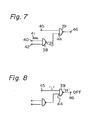
- a first example of the circuit is illustrated in F ig. 7.
- This circuit comprises a first NAND circuit 38 and a second NAND circuit 39.
- An on-and-off signal 41 is introduced into an input terminal 40 of the first NAND circuit 38.
- a bubble actuating signal is introduced into the other input terminal 42.
- the output terminal of the first NAND circuit 38 is connected to an input terminal 44 of the second NAND circuit 39.
- a cassette connection signal is introduced into the other input terminal 45 of the second NAND circuit 39.
- the output terminal 46 of the second NAND circuit 39 is connected to a circuit for actuating a displaying lamp which is not illustrated in this drawing.
- Fig. 8 represents a condition in which the cassette is not inserted and the bubble actuating signal is not introduced.
- a signal of "L” level is introduced into the input terminal 45 of the second NAND circuit 39. Therefore, the output signal from the output terminal 46 of the second NAND circuit 39 is "H" level irrespective of the signal introduced to the other input terminal 44.
- the circuit for actuating the displaying lamp is constructed so that the signal of "H" level from the second NAND circuit turns off the lamp. Therefore, in this condition, the lamp is turned off.
- the actuating signal and the on-off signal 41 are simultaneously, introduced to the first NAND circuit 38. Therefore, the signal of "H” level is introduced to the input terminal 42 and the signal of "L ⁇ H” level is introduced to the other input terminal 40 of the first NAND circuit as illustrated in Fig. 10. Accordingly, the level of the output signal from the first NAND circuit is "H.L” level which is inverted from the on-and-off signal of "L ⁇ H” level. The output signal of "H.L” level is introduced to the input terminal 44 of the second NAND circuit 39. The cassette connection signal of "H” level is already introduced to the input terminal 45 of the second NAND circuit 39. Therefore, an on-and-off signal of "L.H” level is transmitted from the output terminal 46 of the second NAND circuit 39, by which the displaying lamp is turned on and off repeatedly.
- Fig. 11 represents another example of the circuit diagram for displaying whether the cassette is inserted and whether the cassette is being operated.
- a resistance 49, switches 47 and 48, and lamp 51 are connected in series to a power source +V.
- Another resistance 50 is connected between the power source +V and the portion between the two switches 47 and 48.
- the switch 47 is actuated by the bubble actuating signal.
- the other switch 48 is actuated by the cassette connection signal.
- the value of the resistance 49 is about the same as the value of the resistance 50.
- this circuit is as follows.
- the switch 48 is turned off so that the lamp 51 is turned off.
- the cassette connection signal makes the switch 48 turn on. Therefore, current flows through the lamp 51, through the resistance 50 and the switch 48. Luminous intensity of the lamp 51 is low in this condition.
- the bubble actuating signal makes the switch 47 turn on so that the resistance 49 is connected to the resistance 50 in parallel. Therefore, the luminous intensity of the lamp 51 is increased since the total value of resistances 49, 50 in parallel is lower than the value of the resistance 50 alone.
- these examples of circuit diagrams display the situation in which the cassette is housed in the holder by lighting the lamp in the first example or by dimly lighting the lamp in the second example. Also, these circuits make it possible to display the situation in which the cassette is operated by turning the lamp on and off in the first example or by enhancing the luminous intensity of the lamp in the second example. Therefore, it is possible to avoid disconnection of the cassette by pulling out the cassette from the holder.while it is operated. Therefore, data memorized in the bubble chip are normally retained.
Landscapes
- Engineering & Computer Science (AREA)
- Microelectronics & Electronic Packaging (AREA)
- Techniques For Improving Reliability Of Storages (AREA)
Applications Claiming Priority (2)
| Application Number | Priority Date | Filing Date | Title |
|---|---|---|---|
| JP1980123080U JPS618471Y2 (de) | 1980-09-01 | 1980-09-01 | |
| JP123080/80U | 1980-09-01 |
Publications (3)
| Publication Number | Publication Date |
|---|---|
| EP0047167A2 true EP0047167A2 (de) | 1982-03-10 |
| EP0047167A3 EP0047167A3 (en) | 1984-03-21 |
| EP0047167B1 EP0047167B1 (de) | 1989-04-19 |
Family
ID=14851691
Family Applications (1)
| Application Number | Title | Priority Date | Filing Date |
|---|---|---|---|
| EP81303974A Expired EP0047167B1 (de) | 1980-09-01 | 1981-09-01 | Magnetische Blasenspeicheranordnung |
Country Status (4)
| Country | Link |
|---|---|
| US (1) | US4400795A (de) |
| EP (1) | EP0047167B1 (de) |
| JP (1) | JPS618471Y2 (de) |
| DE (1) | DE3177042D1 (de) |
Cited By (3)
| Publication number | Priority date | Publication date | Assignee | Title |
|---|---|---|---|---|
| EP0106474A3 (en) * | 1982-09-06 | 1986-04-02 | Fujitsu Limited | Magnetic bubble casette |
| EP0106726A3 (en) * | 1982-09-10 | 1986-12-30 | Fujitsu Limited | A cassette-type magnetic bubble memory |
| EP0241731A3 (de) * | 1986-03-17 | 1989-04-26 | Nec Corporation | Fassung für elektronisches Gerät |
Families Citing this family (10)
| Publication number | Priority date | Publication date | Assignee | Title |
|---|---|---|---|---|
| JPS5856179B2 (ja) * | 1980-07-15 | 1983-12-13 | ファナック株式会社 | ポ−タブル・バブル・メモリ装置 |
| JPS5894198U (ja) * | 1981-12-18 | 1983-06-25 | 富士通株式会社 | カセット状磁気バブルメモリ装置 |
| JPS58118078A (ja) * | 1981-12-29 | 1983-07-13 | Fanuc Ltd | メモリカセツトの信号・電源供給方式 |
| FR2548815B1 (fr) * | 1983-07-07 | 1988-07-15 | Sagem | Ensemble constitue par un appareil, notamment de lecture et/ou d'ecriture, et par une cassette amovible, notamment contenant une memoire, pour cet appareil et application aux lecteurs de cassettes a memoire a bulles |
| JPS6031800U (ja) * | 1983-08-06 | 1985-03-04 | 富士通株式会社 | カセット式磁気バブルメモリ装置 |
| JPS60212891A (ja) * | 1984-04-09 | 1985-10-25 | Fujitsu Ltd | カセツト式磁気バブルメモリ装置 |
| US4835739A (en) * | 1987-08-04 | 1989-05-30 | Grumman Aerospace Corporation | Mass storage bubble memory system |
| US4931990A (en) * | 1987-11-19 | 1990-06-05 | Bruce C. Perkin | Hardened bubble memory circuit |
| US7345373B2 (en) * | 2005-11-29 | 2008-03-18 | General Electric Company | System and method for utility and wind turbine control |
| CN112876996A (zh) | 2012-10-09 | 2021-06-01 | 艾利丹尼森公司 | 胶黏剂和相关方法 |
Family Cites Families (3)
| Publication number | Priority date | Publication date | Assignee | Title |
|---|---|---|---|---|
| FR1255844A (fr) * | 1959-05-16 | 1961-03-10 | Bassani Spa | Interrupteur de sûreté |
| US3575482A (en) * | 1969-06-05 | 1971-04-20 | Rex Chainbelt Inc | Self-adjusting positive locking chassis latch |
| US4459679A (en) * | 1979-10-04 | 1984-07-10 | Fujitsu Limited | Magnetic bubble memory device cassette |
-
1980
- 1980-09-01 JP JP1980123080U patent/JPS618471Y2/ja not_active Expired
-
1981
- 1981-08-28 US US06/297,265 patent/US4400795A/en not_active Expired - Lifetime
- 1981-09-01 DE DE8181303974T patent/DE3177042D1/de not_active Expired
- 1981-09-01 EP EP81303974A patent/EP0047167B1/de not_active Expired
Cited By (3)
| Publication number | Priority date | Publication date | Assignee | Title |
|---|---|---|---|---|
| EP0106474A3 (en) * | 1982-09-06 | 1986-04-02 | Fujitsu Limited | Magnetic bubble casette |
| EP0106726A3 (en) * | 1982-09-10 | 1986-12-30 | Fujitsu Limited | A cassette-type magnetic bubble memory |
| EP0241731A3 (de) * | 1986-03-17 | 1989-04-26 | Nec Corporation | Fassung für elektronisches Gerät |
Also Published As
| Publication number | Publication date |
|---|---|
| EP0047167B1 (de) | 1989-04-19 |
| JPS5749799U (de) | 1982-03-20 |
| EP0047167A3 (en) | 1984-03-21 |
| JPS618471Y2 (de) | 1986-03-15 |
| DE3177042D1 (en) | 1989-05-24 |
| US4400795A (en) | 1983-08-23 |
Similar Documents
| Publication | Publication Date | Title |
|---|---|---|
| EP0047167A2 (de) | Magnetische Blasenspeicheranordnung | |
| US4891727A (en) | Memory device | |
| US4733314A (en) | Disc unit including automatic ejection upon misinsertion detection | |
| KR880011765A (ko) | 카세트 장착 장치 | |
| EP0027337B1 (de) | Magnetische Blasenspeichervorrichtung | |
| US6332578B1 (en) | Adapter | |
| JPH10135669A (ja) | 電子機器 | |
| CA1189619A (en) | Cassette-type magnetic-bubble memory apparatus | |
| US4445199A (en) | Portable bubble memory apparatus | |
| US3984871A (en) | Tape cartridge release assembly | |
| US6907314B2 (en) | Inventory control device | |
| JPS63282989A (ja) | メモリ−カ−トリツジのドライブ装置 | |
| JPS6113315B2 (de) | ||
| KR19980703443A (ko) | 카드매체의 배출 보호장치 | |
| JPS5942393B2 (ja) | 電気接続体 | |
| KR20010085945A (ko) | 기록 및/또는 재생장치 및 기억매체의 로딩방법 | |
| JP2665212B2 (ja) | Icカードリーダーライター | |
| KR840005883A (ko) | 카세트형 자기 바블 메모리 | |
| JPS56143559A (en) | Cassette magnetic recording and reproducing device | |
| GB2212968A (en) | Cassette tape recorder | |
| KR930004914Y1 (ko) | 자동차용 오토리버스 풀로직 데크의 스위치장치 | |
| CA2000477A1 (en) | High density disk drive with magnetic clutch and a removable cartridge | |
| JP2697184B2 (ja) | Icカードシステム | |
| JP2742339B2 (ja) | 記憶媒体ドライブ装置 | |
| JPS6025757Y2 (ja) | 磁気バブルメモリ装置 |
Legal Events
| Date | Code | Title | Description |
|---|---|---|---|
| PUAI | Public reference made under article 153(3) epc to a published international application that has entered the european phase |
Free format text: ORIGINAL CODE: 0009012 |
|
| AK | Designated contracting states |
Designated state(s): DE FR GB |
|
| PUAL | Search report despatched |
Free format text: ORIGINAL CODE: 0009013 |
|
| AK | Designated contracting states |
Designated state(s): DE FR GB |
|
| 17P | Request for examination filed |
Effective date: 19840822 |
|
| GRAA | (expected) grant |
Free format text: ORIGINAL CODE: 0009210 |
|
| AK | Designated contracting states |
Kind code of ref document: B1 Designated state(s): DE FR GB |
|
| REF | Corresponds to: |
Ref document number: 3177042 Country of ref document: DE Date of ref document: 19890524 |
|
| ET | Fr: translation filed | ||
| PLBE | No opposition filed within time limit |
Free format text: ORIGINAL CODE: 0009261 |
|
| STAA | Information on the status of an ep patent application or granted ep patent |
Free format text: STATUS: NO OPPOSITION FILED WITHIN TIME LIMIT |
|
| 26N | No opposition filed | ||
| PGFP | Annual fee paid to national office [announced via postgrant information from national office to epo] |
Ref country code: FR Payment date: 19920929 Year of fee payment: 12 |
|
| PGFP | Annual fee paid to national office [announced via postgrant information from national office to epo] |
Ref country code: DE Payment date: 19921125 Year of fee payment: 12 |
|
| PG25 | Lapsed in a contracting state [announced via postgrant information from national office to epo] |
Ref country code: FR Free format text: LAPSE BECAUSE OF NON-PAYMENT OF DUE FEES Effective date: 19940531 |
|
| PG25 | Lapsed in a contracting state [announced via postgrant information from national office to epo] |
Ref country code: DE Effective date: 19940601 |
|
| REG | Reference to a national code |
Ref country code: FR Ref legal event code: ST |
|
| PGFP | Annual fee paid to national office [announced via postgrant information from national office to epo] |
Ref country code: GB Payment date: 19940823 Year of fee payment: 14 |
|
| PG25 | Lapsed in a contracting state [announced via postgrant information from national office to epo] |
Ref country code: GB Effective date: 19950901 |
|
| GBPC | Gb: european patent ceased through non-payment of renewal fee |
Effective date: 19950901 |
|
| APAH | Appeal reference modified |
Free format text: ORIGINAL CODE: EPIDOSCREFNO |