EP0047395A2 - Dispositif pour décapage ionique réactif - Google Patents
Dispositif pour décapage ionique réactif Download PDFInfo
- Publication number
- EP0047395A2 EP0047395A2 EP81106090A EP81106090A EP0047395A2 EP 0047395 A2 EP0047395 A2 EP 0047395A2 EP 81106090 A EP81106090 A EP 81106090A EP 81106090 A EP81106090 A EP 81106090A EP 0047395 A2 EP0047395 A2 EP 0047395A2
- Authority
- EP
- European Patent Office
- Prior art keywords
- anode
- baffle plate
- plasma
- chamber
- etching
- Prior art date
- Legal status (The legal status is an assumption and is not a legal conclusion. Google has not performed a legal analysis and makes no representation as to the accuracy of the status listed.)
- Granted
Links
Images

Classifications
-
- H—ELECTRICITY
- H01—ELECTRIC ELEMENTS
- H01J—ELECTRIC DISCHARGE TUBES OR DISCHARGE LAMPS
- H01J37/00—Discharge tubes with provision for introducing objects or material to be exposed to the discharge, e.g. for the purpose of examination or processing thereof
- H01J37/32—Gas-filled discharge tubes
- H01J37/32431—Constructional details of the reactor
- H01J37/32623—Mechanical discharge control means
- H01J37/32633—Baffles
Definitions
- the present invention relates to reactive ion etching and, more particularly, to a reactive ion etching system using a modified reaction chamber which gives uniform silicon etching in batch processing silicon wafers.
- Reactive ion etching has been shown to be widely applicable to a variety of thin film materials and compatible with commonly utilized photoresist systems.
- RIE reactive ion etching
- one of the difficulties encountered in RIE has been obtaining etch rate uniformities suitable for manufacturing semiconductor devices.
- Non-uniformity of etching has been addressed in a variety of prior art etching devices.
- U.S. Patent 4 148 705 to Battey et al describes a plasma etching reactor arrangement for etching, for example, aluminum wherein the plasma is generated between a pair of closely spaced electrodes and a distributed impedance is provided in series with the plasma to assure uniform distribution of the ionizing current and the glow discharge of the plasma throughout the region between the electrodes.
- Galicki et al describe in the IBM Technical Disclosure Bulletin, Vol. 20, No. 6, November 1977, a plasma etch reaction chamber arrangement which provides a uniform flow of gas in the chamber.
- a reactive ion etching chamber arrangement for the selective etching of silicon dioxide has been described by L. M. Ephrath in J. Electrochemical Soc.: Solid-State Science and Technology, August 1979, pp. 1419-1421.
- Ephrath employs for the wafers an aluminum plate which is mechanically and electrically connected to a water cooled RF cathode.
- a grounded counterelectrode is placed in close proximity to the surface of the wafers to reduce the backscattering of aluminum.
- a further plasma etch reaction chamber that attempts to achieve gas uniformity in a batch wafer processing arrangement is that described by Yamamoto et al in U.S. Patent 4 151 034.
- etch rate uniformity becomes even more of a problem because of the larger areas involved.
- the etch rate of materials like silicon can be relatively non-uniform.
- a non-uniformity of 35 percent has been observed in batch processing silicon wafers in a multi-wafer etching mode involving a dozen or more wafers. This non-uniformity of etch rate can occur even though the partial pressure of the injected gas, as well as the plasma density of the etching plasma, is uniform over the chamber volume.
- etch rate is that although the etchant species is generated uniformly over the entire chamber volume/surface, the dominant loss occurs at the target, and thus an etchant species concentration gradient is created which leads to an enhanced etch rate at the outer edge of the target.
- the invention provides a remedy.
- the invention achieves uniform etching of batches of silicon substrates in an enlarged RIE chamber by providing a mechanism within the chamber for adjusting the etchant species concentration across the target so as to be uniform.
- the mechanism is comprised of a plasma enhancing baffle plate (PEBP) placed in the general region above the target in such a way that it encloses a plasma volume between itself and the anode (non-target electrode).
- This enclosed volume is connected to the main chamber volume by providing apertures in the PEBP of various sizes, shapes and locations.
- the concentration of etchant species in the target region in the presence of the PEBP represents a significant increase over that with no plate.
- the PBEP increases the RF currents and, hence, ionizing currents in the region near the PEBP.
- these currents since these currents must pass through the apertures in the PEBP, they are constricted in the region of the apertures leading to a high rate of etchant species production at the aperture locations.
- By adjusting aperture size and location / the etchant species density may be varied over the target to produce a uniform etch rate.
- FIG. 1 shows a typical prior art RIE chamber 1 employing a "tophat” cathode target arrangement.
- anode 3 with interior surface 4 is grounded and cathode top plate 13 of cathode assembly 5 is coupled to RF source 7.
- the "tophat” cathode target assembly arrangement comprises a rounded brim portion 9 integral with wall portion 11 extending upwardly into the RIE chamber.
- Top plate 13 of the "tophat” is electrically insulated from wall portion 11 by insulating spacer 15 and held in place by screws, one of which is shown at 17.
- a seal between the interior of the RIE chamber and atmosphere is achieved via 0-rings 19 and 21 on opposing sides of spacer 15.
- a seal between the interior of the chamber and atmosphere around the brim portion of the "tophat” is achieved via 0-ring 23.
- pallet 27 rests upon top plate 13 and accommodates a plurality of workpieces 25, the latter typically being silicon substrates.
- Pumpdown of the chamber is achieved through port 29 which is separated from the main chamber volume by screen 30.
- the gas inlet 31 and gas ring 33 permit introduction and distribution of the appropriate process gas into the chamber.
- a plasma glow will exist within the interior plasma region 34 of chamber 1.
- the explanation to follow divides the interior chamber plasma region into central plasma region 34A situated over cathode 13 and outer plasma region 34B situated nearer the chamber walls.
- plasma is separated from the inside chamber surfaces, including the surfaces of pallet 27, screen 30 and chamber wall 36, by a plasma sheath.
- the character of the plasma sheath is determined by its particular location within the chamber.
- the cathode plasma sheath 37 is the widest (typically 1 cm), has a high potential drop across it (typically 300 500 V DC ) and is normally observed as a distinct dark region between the cathode and the plasma glow.
- the anode plasma sheath 38 and the wall plasma sheath 39 are generally the same for the system as configured, with a thickness typically ⁇ 1 mm and voltage drop of m 20V.
- the various dark spaces merge continuously into each other, as depicted near cathode edge 40.
- a plasma sheath also exists around gas inlet 31.
- FIG. 2 shows the prior art RIE chamber shown in Figure 1, modified in accordance with the present invention to include the plasma enhancing baffle plate (PEBP) 41 with upper surface 41A and lower surface 41B.
- PEBP plasma enhancing baffle plate
- the gas inlet ring 33 has been omitted, but it is to be understood that the ring or some like form of gas introduction/distribution mechanism is provided within the chamber.
- the particular PEBP shown in Figure 2 has a single large aperture 45 connecting the enclosed plasma region 43 to the plasma region 34A. Aperture 45 permits the creation of an enclosed plasma in region 43 resulting in an anode plasma sheath 44 at both the surface of plate 3 and the upper surface 41A of the PEBP.
- a sheath is formed on lower surface 41B of the PEBP.
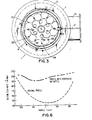
- FIG 3 shows, as an example, a top view of a typical baffle plate arrangement, such arrangement having more particular aperture design detail over that shown in Figure 2.
- the PEBP apertures decrease in size radially, there being one large aperture 45 at the central region of the plate, akin to the PEBP of Figure 2.
- Concentric with the central aperture 45 is a set of six apertures 46A ⁇ 46F,each being approximately three- sevenths in size to that of the central aperture.
- Also indicated by dashed circles is a possible wafer arrangement for RIE processing of a nineteen wafer batch. It should be understood that the arrangement of wafers is for illustration only and does not imply any fixed relationship between the wafer arrangement and the aperture pattern. In fact, any wafer arrangement occupying the same general area of the cathode would suffice for the purpose of this invention.
- the relative sizes, shapes, density and pattern arrangement of PEBP apertures may be varied in accordance with the particular characteristics of the RIE chamber for which the PEBP is designed.
- asymmetric pattern arrangements of apertures, or arrangements for which the hole sizes vary with radius are within the scope of this invention.
- an aperture arrangement or configuration is not necessarily unique for a given chamber but is to be designed such that it optimally compensates for the non-uniformity in etch rate of the particular chamber for which it is intended to be used.
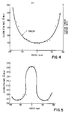
- Figure 4 shows, as an example, the plot of the expected neutral fluorine concentration profile (F Concent.) across the cathode target 13 in the RIE apparatus shown in Figure 1 under the conditions of etching silicon with CF 4 .
- This profile was obtained through numerical calculation by assuming that fluorine is produced at a constant rate S in the entire plasma region 34A-34B of Figure 1 by electron collisions with the gas CF 4 injected through gas feed 31, and that fluorine is only removed by combining with silicon to form S i F X at the silicon wafers 25 on target cathode 13 or, alternatively, at the surface of pallet 27 where latter is, for example, constructed of silicon.
- the shape of the fluorine concentration curve shown in Figure 4 may be explained by the following simple model. Fluorine is produced everywhere within the plasma regions 34A and 34B shown in Figure 1. Under steady state situations, the fluorine produced in region 34B must diffuse into the target region 34A, where it is eventually removed by combining with the silicon. In order for this diffusion to occur, a fluorine concentration gradient is set up with the fluorine concentration increasing radially out from the center of target cathode 13.
- RIE reactive ion etching
- etch rate of the ion component versus the neutral component in an RIE etch system will depend strongly on the etchant gas and the material being etched. For example, in RIE of silicon in a CF 4 plasma, the etch rate depends strongly on the fluorine concentration (or other active fluorine radicals) while in RIE of SiO 2 in a CF 4 plasma the etch rate is dominated by ionic (most likely CF3) concentration and depends much less on the neutral fluorine concentration.
- etch rate non-uniformity due to concentration gradients of neutral etching species is directed to the example of etching silicon using CF 4
- the problem of etch rate non-uniformity due to concentration gradients of neutral etching species is general to any similar etching process, i.e. one for which the etch rate depends on the presence of a neutral species produced within the plasma.
- the etch rate will be proportional to the neutral species density.
- Figure 4 also shows measured etch rate points using silicon wafers and CF 4 as the etchant gas. Measurements were made (three measurement points per wafer) on five wafers arrayed along a diameter of a cylindrical target cathode, similar to that shown in Figure 1. These etch rate points were obtained using a pressure of 40 ⁇ m Hg, a flow rate of 25 SCCM (Standard cm 3 per minute), an RF power of 400 W and an RF frequency of about 13.56 MHz. The batch uniformity in etching silicon under such conditions was found to be + 39 percent. As can be seen, the series of points representing the measured silicon etch rate at various radial points on the cathode surface follow closely the calculated neutral fluorine concentration profile.
- the PEBP is positioned in relatively close proximity to anode 3 to form region 43.
- the distance between the anode and PEBP may vary up to a distance equal to 25 percent of the PEBP diameter but should, in no event, be more than 50 percent of the distance between anode and cathode.
- the spacing between anode and PEBP should be no more than 127 mm (5 inches) but in no event more than half the distance from anode to cathode.
- the minimum distance or spacing between anode and PEBP should be no less than 10 to 20 Debye lengths since spacing less than this will start to extinguish the plasma.
- a typically good operating distance between anode and PEBP is approximately 25.4 mm (1 inch).
- FIG. 5 shows a measured etch rate profile where a PEBP with only one large central perforation is employed, such perforation being akin to perforation 45 in Figure 3.
- the etch rate sharply peaks to approximately 0 230A per minute at the central point of the cathode target, there being a sharp drop-off in etch rate approximately 50.8 mm (2 inches) from the center of the target.
- a PEBP aperture diameter of from 38.1 to 50.8 mm (1.5 to 2 inches) with the high etch values observed on the target at the point opposite the center of the aperture.
- this enhanced etch rate is apparently due to an increased etchant concentration in the target region beneath the aperture. The reason for this is postulated as follows.
- One condition necessary for this enhanced plasma glow to occur is that the PEBP has apertures with opening dimensions considerably greater than the plasma Debye length. Under such a condition, the plasmas in regions 43 and 34 are closely coupled and the anode area of the system is increased by the total surface area of the PEBP 41. This has two effects.
- apertures now represent an enhanced source of etchant species which may be adjusted over the target area by adjusting aperture locations, number and sizes. It is clear that, in accordance with the above teachings, the effect of aperture arrangement on etchant species may be calculated and the aperture designed to produce high etch rate uniformity in accordance with the particular characteristics of the system.
- Figure 6 shows a silicon etch rate profile both with and without the use of a PEBP.
- the silicon etch rate profile without the use of the PEBP is designated "original profile" in Figure 6.
- the profile characteristic shown in Figure 6 with the use of the PEBP represents the results obtained using a baffle plate akin to that shown in Figure 3, typically a plate 20 inches in diameter in a 28-inch diameter chamber.
- a cathode target of 508 mm (20 inches) is employed and, as shown in Figure 3, 19 silicon wafers of, for example, 82 mm dimension are closed-packed in the central region of the target cathode.
- An interelectrode spacing of approximately 76.2 mm (3.5 inches) was utilized and the initial evacuation level typically would be 5 X 10 torr.
- the concentric rings of perforations extending outwardly from central perforation 45 act to spread or flatten the etch rate profile shown in Figure 5 wherein only perforation 45 was employed.
- the distribution of the etchant species caused by the perforations is further spread outwardly from the center of the target in a manner to compensate for the deficiency of species in prior art RIE chambers, as depicted by the profile in Figure 4. Accordingly, this compensation acts to cause the etch rate to be more nearly uniform over the radius of the cathode target, as shown in Figure 6.
- baffle configurations may be designed to meet particular applications whereby the etch rate over the entire cathode target may be made optimally uniform.
- specific parameters have been given in the examples above, it is clear that different etchant species, flow rates, chamber pressures and RF power levels may be utilized.
- the plasma enhancing baffle plate may as readily be employed to attain enhanced uniformity in any etching application in which the neutral species component has an appreciable effect.
Landscapes
- Physics & Mathematics (AREA)
- Engineering & Computer Science (AREA)
- Plasma & Fusion (AREA)
- Chemical & Material Sciences (AREA)
- Analytical Chemistry (AREA)
- Drying Of Semiconductors (AREA)
Applications Claiming Priority (2)
| Application Number | Priority Date | Filing Date | Title |
|---|---|---|---|
| US185831 | 1980-09-10 | ||
| US06/185,831 US4340461A (en) | 1980-09-10 | 1980-09-10 | Modified RIE chamber for uniform silicon etching |
Publications (3)
| Publication Number | Publication Date |
|---|---|
| EP0047395A2 true EP0047395A2 (fr) | 1982-03-17 |
| EP0047395A3 EP0047395A3 (en) | 1982-04-07 |
| EP0047395B1 EP0047395B1 (fr) | 1984-03-21 |
Family
ID=22682620
Family Applications (1)
| Application Number | Title | Priority Date | Filing Date |
|---|---|---|---|
| EP81106090A Expired EP0047395B1 (fr) | 1980-09-10 | 1981-08-04 | Dispositif pour décapage ionique réactif |
Country Status (4)
| Country | Link |
|---|---|
| US (1) | US4340461A (fr) |
| EP (1) | EP0047395B1 (fr) |
| JP (1) | JPH0359573B2 (fr) |
| DE (1) | DE3162803D1 (fr) |
Cited By (4)
| Publication number | Priority date | Publication date | Assignee | Title |
|---|---|---|---|---|
| EP0200133A3 (en) * | 1985-05-01 | 1987-12-16 | International Business Machines Corporation | Plasma etching reactor |
| EP0282836A3 (en) * | 1987-03-20 | 1989-07-26 | Leybold Aktiengesellschaft | Process and apparatus for depositing of high ohmic resistance layers by cathodic sputtering |
| EP0395017A3 (fr) * | 1989-04-25 | 1990-12-19 | Tokyo Electron Limited | Méthode d'attaque par plasma |
| GB2327909A (en) * | 1997-08-07 | 1999-02-10 | Bosch Gmbh Robert | Anisotropic plasma etching of a silicon wafer with aperture between plasma source and wafer |
Families Citing this family (15)
| Publication number | Priority date | Publication date | Assignee | Title |
|---|---|---|---|---|
| US4384938A (en) * | 1982-05-03 | 1983-05-24 | International Business Machines Corporation | Reactive ion etching chamber |
| US4534816A (en) * | 1984-06-22 | 1985-08-13 | International Business Machines Corporation | Single wafer plasma etch reactor |
| US4595484A (en) * | 1985-12-02 | 1986-06-17 | International Business Machines Corporation | Reactive ion etching apparatus |
| NL8601824A (nl) * | 1986-07-11 | 1988-02-01 | Hauzer Holding | Werkwijze en inrichting voor het met een geleidend plasmakanaal ontsteken van een boog. |
| US5015331A (en) * | 1988-08-30 | 1991-05-14 | Matrix Integrated Systems | Method of plasma etching with parallel plate reactor having a grid |
| US5002631A (en) * | 1990-03-09 | 1991-03-26 | At&T Bell Laboratories | Plasma etching apparatus and method |
| US5451435A (en) * | 1990-06-18 | 1995-09-19 | At&T Corp. | Method for forming dielectric |
| US5415753A (en) * | 1993-07-22 | 1995-05-16 | Materials Research Corporation | Stationary aperture plate for reactive sputter deposition |
| US5711849A (en) * | 1995-05-03 | 1998-01-27 | Daniel L. Flamm | Process optimization in gas phase dry etching |
| US6500314B1 (en) * | 1996-07-03 | 2002-12-31 | Tegal Corporation | Plasma etch reactor and method |
| US6048435A (en) | 1996-07-03 | 2000-04-11 | Tegal Corporation | Plasma etch reactor and method for emerging films |
| US6203661B1 (en) * | 1999-12-07 | 2001-03-20 | Trusi Technologies, Llc | Brim and gas escape for non-contact wafer holder |
| JP4370789B2 (ja) * | 2002-07-12 | 2009-11-25 | 東京エレクトロン株式会社 | プラズマ処理装置及び可変インピーダンス手段の校正方法 |
| KR100661186B1 (ko) * | 2005-03-23 | 2006-12-22 | 주식회사 하이닉스반도체 | 플래쉬 메모리 소자의 제조방법 |
| US20090095714A1 (en) * | 2007-10-12 | 2009-04-16 | Tokyo Electron Limited | Method and system for low pressure plasma processing |
Family Cites Families (18)
| Publication number | Priority date | Publication date | Assignee | Title |
|---|---|---|---|---|
| US3282815A (en) * | 1963-07-01 | 1966-11-01 | Ibm | Magnetic control of film deposition |
| US3410774A (en) * | 1965-10-23 | 1968-11-12 | Ibm | Method and apparatus for reverse sputtering selected electrically exposed areas of a cathodically biased workpiece |
| US3480535A (en) * | 1966-07-07 | 1969-11-25 | Trw Inc | Sputter depositing semiconductor material and forming semiconductor junctions through a molten layer |
| US3733258A (en) * | 1971-02-03 | 1973-05-15 | Rca Corp | Sputter-etching technique for recording holograms or other fine-detail relief patterns in hard durable materials |
| GB1417085A (en) * | 1973-05-17 | 1975-12-10 | Standard Telephones Cables Ltd | Plasma etching |
| FR2265872B1 (fr) * | 1974-03-27 | 1977-10-14 | Anvar | |
| IT1203089B (it) * | 1976-03-03 | 1989-02-15 | Int Plasma Corp | Procedimento ed apparecchiatura per eseguire reazioni chimiche nella regione della scarica luminescente di un plasma |
| DE2644208C3 (de) * | 1976-09-30 | 1981-04-30 | Siemens AG, 1000 Berlin und 8000 München | Verfahren zur Herstellung einer einkristallinen Schicht auf einer Unterlage |
| DE2709107A1 (de) * | 1977-03-02 | 1978-09-07 | Siemens Ag | Verfahren zum einebnen mikroskopischer rauhigkeiten in der oberflaeche eines festkoerpersubstrates |
| JPS5450440A (en) * | 1977-09-29 | 1979-04-20 | Cho Lsi Gijutsu Kenkyu Kumiai | Plasma etching device |
| US4119881A (en) * | 1978-02-27 | 1978-10-10 | Control Data Corporation | Ion beam generator having concentrically arranged frustoconical accelerating grids |
| JPS54128284A (en) * | 1978-03-29 | 1979-10-04 | Kokusai Electric Co Ltd | Electrode structure for semiconductor wafer plasma etching stripping device |
| US4230515A (en) * | 1978-07-27 | 1980-10-28 | Davis & Wilder, Inc. | Plasma etching apparatus |
| US4211601A (en) * | 1978-07-31 | 1980-07-08 | Bell Telephone Laboratories, Incorporated | Device fabrication by plasma etching |
| US4183780A (en) * | 1978-08-21 | 1980-01-15 | International Business Machines Corporation | Photon enhanced reactive ion etching |
| JPS5539690A (en) * | 1978-09-14 | 1980-03-19 | Chiyou Lsi Gijutsu Kenkyu Kumiai | Plasma etching device |
| US4209357A (en) * | 1979-05-18 | 1980-06-24 | Tegal Corporation | Plasma reactor apparatus |
| JPS6053751B2 (ja) * | 1979-12-10 | 1985-11-27 | 松下電子工業株式会社 | プラズマ処理装置 |
-
1980
- 1980-09-10 US US06/185,831 patent/US4340461A/en not_active Expired - Lifetime
-
1981
- 1981-07-20 JP JP56112407A patent/JPH0359573B2/ja not_active Expired - Lifetime
- 1981-08-04 EP EP81106090A patent/EP0047395B1/fr not_active Expired
- 1981-08-04 DE DE8181106090T patent/DE3162803D1/de not_active Expired
Cited By (7)
| Publication number | Priority date | Publication date | Assignee | Title |
|---|---|---|---|---|
| EP0200133A3 (en) * | 1985-05-01 | 1987-12-16 | International Business Machines Corporation | Plasma etching reactor |
| EP0282836A3 (en) * | 1987-03-20 | 1989-07-26 | Leybold Aktiengesellschaft | Process and apparatus for depositing of high ohmic resistance layers by cathodic sputtering |
| EP0395017A3 (fr) * | 1989-04-25 | 1990-12-19 | Tokyo Electron Limited | Méthode d'attaque par plasma |
| US5089083A (en) * | 1989-04-25 | 1992-02-18 | Tokyo Electron Limited | Plasma etching method |
| GB2327909A (en) * | 1997-08-07 | 1999-02-10 | Bosch Gmbh Robert | Anisotropic plasma etching of a silicon wafer with aperture between plasma source and wafer |
| GB2327909B (en) * | 1997-08-07 | 2000-03-08 | Bosch Gmbh Robert | Process and device for the anisotropic etching of substrates |
| US6214161B1 (en) | 1997-08-07 | 2001-04-10 | Robert Bosch Gmbh | Method and apparatus for anisotropic etching of substrates |
Also Published As
| Publication number | Publication date |
|---|---|
| EP0047395B1 (fr) | 1984-03-21 |
| EP0047395A3 (en) | 1982-04-07 |
| DE3162803D1 (en) | 1984-04-26 |
| JPH0359573B2 (fr) | 1991-09-11 |
| US4340461A (en) | 1982-07-20 |
| JPS5754324A (fr) | 1982-03-31 |
Similar Documents
| Publication | Publication Date | Title |
|---|---|---|
| EP0047395B1 (fr) | Dispositif pour décapage ionique réactif | |
| US4600464A (en) | Plasma etching reactor with reduced plasma potential | |
| US7138067B2 (en) | Methods and apparatus for tuning a set of plasma processing steps | |
| JP6854768B2 (ja) | 周期的かつ選択的な材料の除去及びエッチングのための処理チャンバ | |
| CN100401450C (zh) | 中空阳极等离子体反应器与方法 | |
| US5605637A (en) | Adjustable dc bias control in a plasma reactor | |
| US5310454A (en) | Dry etching method | |
| US4380488A (en) | Process and gas mixture for etching aluminum | |
| GB2026369A (en) | Plasma etching apparatus | |
| KR20010089689A (ko) | 플라즈마 리액터 내의 천공된 플라즈마 한정 링 | |
| US4400235A (en) | Etching apparatus and method | |
| US4424102A (en) | Reactor for reactive ion etching and etching method | |
| US6827870B1 (en) | Method and apparatus for etching and deposition using micro-plasmas | |
| US4810322A (en) | Anode plate for a parallel-plate reactive ion etching reactor | |
| WO2008049024A1 (fr) | Procédés et appareil permettant de régler une série d'opérations de traitement au plasma | |
| KR20250022790A (ko) | 원격 플라즈마 프로세스들을 위한 식각제들을 생성하기 위한 장치 | |
| US20250046629A1 (en) | Ion beam etching apparatus, method for manufacturing semiconductor device using the same, and method for treating substrate using the same | |
| KR20250116060A (ko) | 에칭 방법 및 플라즈마 처리 장치 | |
| WO2001027969A1 (fr) | Procede et dispositif d'attaque et de depot au moyen de micro-plasmas | |
| US5681419A (en) | Reactive ion etching apparatus | |
| KR20050001831A (ko) | 플라즈마 처리 장치 | |
| JPS6032972B2 (ja) | エツチング装置 | |
| US20250174462A1 (en) | Substrate processing method and substrate processing system | |
| KR20250020257A (ko) | 이온 빔 식각 장치, 이를 이용한 반도체 장치 제조 방법, 및 이를 이용한 기판 처리 방법 | |
| JPS6276627A (ja) | ドライエツチング装置 |
Legal Events
| Date | Code | Title | Description |
|---|---|---|---|
| PUAI | Public reference made under article 153(3) epc to a published international application that has entered the european phase |
Free format text: ORIGINAL CODE: 0009012 |
|
| PUAL | Search report despatched |
Free format text: ORIGINAL CODE: 0009013 |
|
| 17P | Request for examination filed |
Effective date: 19810804 |
|
| AK | Designated contracting states |
Designated state(s): DE FR GB IT |
|
| AK | Designated contracting states |
Designated state(s): DE FR GB IT |
|
| GRAA | (expected) grant |
Free format text: ORIGINAL CODE: 0009210 |
|
| AK | Designated contracting states |
Designated state(s): DE FR GB IT |
|
| PG25 | Lapsed in a contracting state [announced via postgrant information from national office to epo] |
Ref country code: IT Free format text: LAPSE BECAUSE OF FAILURE TO SUBMIT A TRANSLATION OF THE DESCRIPTION OR TO PAY THE FEE WITHIN THE PRESCRIBED TIME-LIMIT;WARNING: LAPSES OF ITALIAN PATENTS WITH EFFECTIVE DATE BEFORE 2007 MAY HAVE OCCURRED AT ANY TIME BEFORE 2007. THE CORRECT EFFECTIVE DATE MAY BE DIFFERENT FROM THE ONE RECORDED. Effective date: 19840321 |
|
| REF | Corresponds to: |
Ref document number: 3162803 Country of ref document: DE Date of ref document: 19840426 |
|
| ET | Fr: translation filed | ||
| PLBE | No opposition filed within time limit |
Free format text: ORIGINAL CODE: 0009261 |
|
| STAA | Information on the status of an ep patent application or granted ep patent |
Free format text: STATUS: NO OPPOSITION FILED WITHIN TIME LIMIT |
|
| 26N | No opposition filed | ||
| PGFP | Annual fee paid to national office [announced via postgrant information from national office to epo] |
Ref country code: FR Payment date: 19910726 Year of fee payment: 11 |
|
| PGFP | Annual fee paid to national office [announced via postgrant information from national office to epo] |
Ref country code: DE Payment date: 19910828 Year of fee payment: 11 |
|
| PGFP | Annual fee paid to national office [announced via postgrant information from national office to epo] |
Ref country code: GB Payment date: 19920722 Year of fee payment: 12 |
|
| PG25 | Lapsed in a contracting state [announced via postgrant information from national office to epo] |
Ref country code: FR Effective date: 19930430 |
|
| PG25 | Lapsed in a contracting state [announced via postgrant information from national office to epo] |
Ref country code: DE Effective date: 19930501 |
|
| REG | Reference to a national code |
Ref country code: FR Ref legal event code: ST |
|
| PG25 | Lapsed in a contracting state [announced via postgrant information from national office to epo] |
Ref country code: GB Effective date: 19930804 |
|
| GBPC | Gb: european patent ceased through non-payment of renewal fee |
Effective date: 19930804 |