EP0047591A2 - Lichtemittierende Diode mit hoher äusserer Quantenausbeute - Google Patents
Lichtemittierende Diode mit hoher äusserer Quantenausbeute Download PDFInfo
- Publication number
- EP0047591A2 EP0047591A2 EP81303706A EP81303706A EP0047591A2 EP 0047591 A2 EP0047591 A2 EP 0047591A2 EP 81303706 A EP81303706 A EP 81303706A EP 81303706 A EP81303706 A EP 81303706A EP 0047591 A2 EP0047591 A2 EP 0047591A2
- Authority
- EP
- European Patent Office
- Prior art keywords
- layer
- light emitting
- emitting diode
- further characterised
- region
- Prior art date
- Legal status (The legal status is an assumption and is not a legal conclusion. Google has not performed a legal analysis and makes no representation as to the accuracy of the status listed.)
- Granted
Links
Images
Classifications
-
- H—ELECTRICITY
- H10—SEMICONDUCTOR DEVICES; ELECTRIC SOLID-STATE DEVICES NOT OTHERWISE PROVIDED FOR
- H10H—INORGANIC LIGHT-EMITTING SEMICONDUCTOR DEVICES HAVING POTENTIAL BARRIERS
- H10H20/00—Individual inorganic light-emitting semiconductor devices having potential barriers, e.g. light-emitting diodes [LED]
- H10H20/80—Constructional details
- H10H20/83—Electrodes
- H10H20/831—Electrodes characterised by their shape
- H10H20/8312—Electrodes characterised by their shape extending at least partially through the bodies
-
- H—ELECTRICITY
- H10—SEMICONDUCTOR DEVICES; ELECTRIC SOLID-STATE DEVICES NOT OTHERWISE PROVIDED FOR
- H10H—INORGANIC LIGHT-EMITTING SEMICONDUCTOR DEVICES HAVING POTENTIAL BARRIERS
- H10H20/00—Individual inorganic light-emitting semiconductor devices having potential barriers, e.g. light-emitting diodes [LED]
- H10H20/01—Manufacture or treatment
- H10H20/011—Manufacture or treatment of bodies, e.g. forming semiconductor layers
- H10H20/018—Bonding of wafers
-
- H—ELECTRICITY
- H10—SEMICONDUCTOR DEVICES; ELECTRIC SOLID-STATE DEVICES NOT OTHERWISE PROVIDED FOR
- H10H—INORGANIC LIGHT-EMITTING SEMICONDUCTOR DEVICES HAVING POTENTIAL BARRIERS
- H10H20/00—Individual inorganic light-emitting semiconductor devices having potential barriers, e.g. light-emitting diodes [LED]
- H10H20/80—Constructional details
- H10H20/81—Bodies
- H10H20/811—Bodies having quantum effect structures or superlattices, e.g. tunnel junctions
-
- H—ELECTRICITY
- H10—SEMICONDUCTOR DEVICES; ELECTRIC SOLID-STATE DEVICES NOT OTHERWISE PROVIDED FOR
- H10H—INORGANIC LIGHT-EMITTING SEMICONDUCTOR DEVICES HAVING POTENTIAL BARRIERS
- H10H20/00—Individual inorganic light-emitting semiconductor devices having potential barriers, e.g. light-emitting diodes [LED]
- H10H20/80—Constructional details
- H10H20/81—Bodies
- H10H20/822—Materials of the light-emitting regions
- H10H20/824—Materials of the light-emitting regions comprising only Group III-V materials, e.g. GaP
-
- H—ELECTRICITY
- H10—SEMICONDUCTOR DEVICES; ELECTRIC SOLID-STATE DEVICES NOT OTHERWISE PROVIDED FOR
- H10H—INORGANIC LIGHT-EMITTING SEMICONDUCTOR DEVICES HAVING POTENTIAL BARRIERS
- H10H20/00—Individual inorganic light-emitting semiconductor devices having potential barriers, e.g. light-emitting diodes [LED]
- H10H20/80—Constructional details
- H10H20/84—Coatings, e.g. passivation layers or antireflective coatings
- H10H20/841—Reflective coatings, e.g. dielectric Bragg reflectors
-
- H—ELECTRICITY
- H10—SEMICONDUCTOR DEVICES; ELECTRIC SOLID-STATE DEVICES NOT OTHERWISE PROVIDED FOR
- H10H—INORGANIC LIGHT-EMITTING SEMICONDUCTOR DEVICES HAVING POTENTIAL BARRIERS
- H10H20/00—Individual inorganic light-emitting semiconductor devices having potential barriers, e.g. light-emitting diodes [LED]
- H10H20/80—Constructional details
- H10H20/81—Bodies
- H10H20/819—Bodies characterised by their shape, e.g. curved or truncated substrates
- H10H20/821—Bodies characterised by their shape, e.g. curved or truncated substrates of the light-emitting regions, e.g. non-planar junctions
-
- H—ELECTRICITY
- H10—SEMICONDUCTOR DEVICES; ELECTRIC SOLID-STATE DEVICES NOT OTHERWISE PROVIDED FOR
- H10H—INORGANIC LIGHT-EMITTING SEMICONDUCTOR DEVICES HAVING POTENTIAL BARRIERS
- H10H20/00—Individual inorganic light-emitting semiconductor devices having potential barriers, e.g. light-emitting diodes [LED]
- H10H20/80—Constructional details
- H10H20/83—Electrodes
- H10H20/832—Electrodes characterised by their material
Definitions
- This invention relates to surface emitting light emitting diodes (LED) with enhanced external quantum efficiency.
- the internal quantum efficiency of surface emitting LED's is of the order of 80 - 100 percent, only 2 - 2.5 percent (top emitters) or 4 - 5 percent (Burrus-type LED's) of the internally generated light can escape from the LED.
- the high refractive index of LED semiconductor material for example GaAlAs, causes total internal reflection for all rays that strike the surface at an angle greater than the critical angle ec. If the light emitting region of the device is considered as a point source emitting into a spherical volume, then only 1/2 of the light is emitted into the positive hemisphere. Of this light, only a fraction Sin2e will strike a given LED surface at less than the critical angle.
- the reflecting layer can, for example, be a layer of silicon dioxide in the thickness range of 1000A to 2000A units coated with a reflective metal, for example, Cr/Au or Ti/Pt.
- the reflective metal is preferably a central part of the second contact metallization, the composition of the contact metallization depending on the carrier type of the underlying semiconductor layer.
- the reflective layer may alternatively comprise a multilayer dielectric, for example, a stack of quarter- wavelength (X/4) layers of A1 2 0 3 and Si.
- the current directing means depends on the particular LED design and on the heterostructure system.
- the structure can include an n-type barrier layer formed on the second confining layer except at a central region thereof in vertical alignment with the emitting region.
- the structure can also incorporate a p-type diffusion layer extending both into the barrier layer and into the second confining layer at said central region.
- the junction of the barrier layer and the second confining layer forms, in operation, a reverse-biased isolating pn junction, current thus being funneled along the p-type diffusion layer and into the second confining layer where the p-type diffusion layer extends into the second confining layer.
- an alternative structure particularly adapted for the InP system has a current confining path defined on one side by a highly conductive second confining layer and on the other side by a reverse-biased annular p-n junction whereby current is directed to a central region of the device.
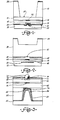
- a surface emitting LED consisting of a GaAlAs heterostructure.
- a first confining layer of n-type Ga 0.78 Al 0.22 As is grown by liquid phase epitaxy on a GaAs substrate 12.
- a 0.1-2 micron active layer 14 of p-type Ga 0.95 Al 0.05 As is then grown on the first confining layer 10.
- a 1-3 micron second confining layer 16 of p-type Ga 0.95 Al 0.05 As is then grown on the active layer 14.
- a 1 micron capping barrier layer 18 of n-type Ga 0.90 Al 0.10 As is then grown on the second confining layer 16.
- the higher aluminum content of this layer compared to the active layer ensures low light absorption.
- a circular window of about 50 microns diameter is opened up in the barrier layer 18 using selective etching procedures. For example, a solution of H202 and NaOH having a pH of about 8 attacks the layer 18 leaving the second confining layer 16 intact.
- an anodic etching technique can be used to produce a window whose boundary is independent of crystallographic planes.
- a zinc diffusion is then carried out over the whole lower surface of the chip to produce a 0.5 - 0.7 micron layer 20 of p-type material over the outer surface of the layer 18, including the boundary surface of the window, and extending into the exposed region of the confining layer 16. This is done by enclosing the chip for 20 minutes in an atmosphere generated by heating a composition of 1g GaAs, lg Ga and 500mg Zn to 600°C in a 250cc ampoule. A 1500A layer of silicon dioxide is then chemically vapor deposited over the upper surface of the chip and is etched using buffered HF to leave a 75 micron diameter dot 22 in alignment with the circular window.
- a Cr/Au metallization contact 24 is then vacuum evaporated over the silicon dioxide dot and a 5-10 micron gold heat sink 26 is plated over the bottom surface of the chip.
- a 200A Au/Ge; 2000A Au contact layer 28 is evaporated onto the top surface of the substrate, a well 30 then being etched into the substrate down to the first confining layer to permit emission of light.
- a current in the range of 1-500mA flows from a bottom contact 24/26 to the top contact 28 through an emitting region 32.
- the emitting region does not lie in a direct line between the top and bottom contacts since the top contact 28 is an annular contact extending around the well 30 and, similarly, the bottom contact 26/24 is an annular contact extending around the relatively high resistance silicon dioxide dot 22. Consequently, current, in passing between the contacts must be funnelled into and away from the emitting region 32. Current entering the bottom contact flows readily into the layers 20 and 18 but will not pass the reverse-biased junction between the barrier layer 18 and the second confining layer 16.
- the current consequently flows towards the centre of the chip to a region 32 where it encounters a zinc diffused conductive region extending into the confining layer 16.
- Current thus flows along the inside surface of the reflecting layer 22 until it can cross into the confining layer and, where it crosses; this defines the region 32 since the path to the active layer 14 from the zinc diffused layer-20 is relatively - low resistance.
- the combination of the silicon dioxide layer 22 and the metallization 24 below the emitting region increases reflectivity significantly over the 0.55 value currently obtained by metallization alone.
- FIG. 2 there is a shown an enhanced external quantum efficiency top emitting LED structure which is particularly adapted for the InP heterostructure.
- InP devices are of growing interest since they emit longer wavelengths compatible with the minimum loss regime of optical fibres.
- the device illustrated in Figure 2 differs from the GaAlAs device illustrated in Figure 1 in that current confinement is solely achieved by the use of potential barriers within the LED chip instead of by external isolation and potential barriers.
- a 1-3 micron layer 38 of n-type InP is grown by liquid phase epitaxy.
- a window 40 is opened in the n-type layer 38 using conventional photolithographic and etching techniques. The diameter of the window 40 corresponds to the desired emitting area of the LED and is in the range of 15-100 microns.
- the p-type substrate 36 is exposed at the wi-ndow 40.
- a double heterostructure layer sequence comprising a first confining layer 42 of 2-3 microns p-type InP, a 0.2-2 micron active layer 44 of p- or n-type GaInAsP and a 1.5-3 micron second confining layer 46 of n-type InP are grown.
- the internal layer 38 provides a reverse biased pn junction in operation and so restricts current flow to the window region 40. As a result, light emission is also restricted to a region 48 of the active layer 44 in vertical alignment with the window 40.
- a 1500A layer of silicon dioxide 50 is deposited over the bottom surface of the second confining layer 46 using chemical vapor deposition.
- the silicon dioxide 50 is photo-engraved to yield dots somewhat larger than the emitting region 48 so as to redirect as much light as possible.
- the silicon dioxide dot is provided with a gold plated heat sink 52 which extends substantially over the whole of the bottom surface of the chip.
- the inner surface of the gold layer forms an annular contact region with the highly conductive n-type InP.
- the bottom contact 32 and a Au/Be 2000A annular top contact 54 do not determine current confinement to the emitting region, and so have relatively large contact areas on both crystal surfaces which provides a low series resistance.
- the current confinement is .ensured by the highly conductive n-type second confining layer 46 which encourages current to move inwardly towards the emitting region 48 and window 40 rather than to cross the reverse-biased pn junction between the first confining layer 42 and the internal layer 38.
- the reflective element 50 ensures an improvement in light output of the order of 3dB.
- a similar structure could be obtained by reversing the carrier types of all the semiconductor materials. However, it is doubtful if significant carrier confinement will result due to the much higher conductivity of n-type InP, so the structure illustrated is preferred.
- the silicon dioxide could be substituted by another suitable dielectric, for example, alumina.
- reflection can be accomplished by a multilayer dielectric of the type described by Ettenberg (Applied Physics Letters Vol. 32 (11) June 1, 1978, pp 724-725).
- the surface emitting GaAs/GaAlAs double heterostructure LED illustrated in Figure 3 is structurally in many respects the inverse of the LED as shown in Figure 1.
- the LED has a substrate 60 of GaAs, a 25 micron first confining layer 62 of n-type GaAlAs, a 0.1-5 micron active layer 64 of p-type GaAs, a 1-3 micron second confining layer 66 of p-type GaAlAs, a 1 micron barrier 68 of n-type GaAlAs, and a 0.5-0.7 micron zinc duffused p-type layer 70, the p-type layer 70 extending into the second confining layer 66 as described with respect to Figure 1.
- the layers 62, 64, 66 and 68 are grown by, for example, liquid phase epitaxy and the recess 74 is opened up using conventional photo-engraving techniques including a selective etchant. Further details of the LPE processing may be found in U.S. Patent Serial No. 4,086,126.
- the substrate is processed by first evaporating a Au/Ge layer 79 onto the substrate surface and then etching a well 80 through to the first confining layer using a selective etchant. Subsequently, a 1000 2000A reflecting layer 82 of silicon dioxide is chemically vapor deposited into the well after first masking the bottom metallization 79. The silica layer 82 is followed by an evaporated layer of Cr/Au 84 to provide thermal contact between the silicon dioxide layer and a subsequently electroplated layer 86 of Au.
- the first confining layer 62 should be 25 microns or greater to ensure a low series resistance for current which is forced to flow outwardly from the emitting region 76 and around the well 82 to reach the bottom metallization 82.
- the essence of the invention is that a light emitting region should be directly between a transmissive element and a reflective element and that the contact metallization at respective sides should be radially outward of these elements.
- the LED should include means for causing currents to converge from the input metallization to the emitting region and to cause the current to diverge from the emitting region to the output metallization. That means can, for example, be a reverse-biased pn junction, a region of enhanced conductivity, or can be merely defined by the geometry of the device.
Landscapes
- Led Devices (AREA)
Applications Claiming Priority (2)
| Application Number | Priority Date | Filing Date | Title |
|---|---|---|---|
| CA000360029A CA1139412A (en) | 1980-09-10 | 1980-09-10 | Light emitting diodes with high external quantum efficiency |
| CA360029 | 1980-09-10 |
Publications (3)
| Publication Number | Publication Date |
|---|---|
| EP0047591A2 true EP0047591A2 (de) | 1982-03-17 |
| EP0047591A3 EP0047591A3 (en) | 1982-09-29 |
| EP0047591B1 EP0047591B1 (de) | 1985-11-21 |
Family
ID=4117853
Family Applications (1)
| Application Number | Title | Priority Date | Filing Date |
|---|---|---|---|
| EP81303706A Expired EP0047591B1 (de) | 1980-09-10 | 1981-08-14 | Lichtemittierende Diode mit hoher äusserer Quantenausbeute |
Country Status (5)
| Country | Link |
|---|---|
| US (1) | US4342944A (de) |
| EP (1) | EP0047591B1 (de) |
| JP (1) | JPS5779688A (de) |
| CA (1) | CA1139412A (de) |
| DE (1) | DE3172987D1 (de) |
Cited By (5)
| Publication number | Priority date | Publication date | Assignee | Title |
|---|---|---|---|---|
| FR2531814A1 (fr) * | 1982-08-10 | 1984-02-17 | Thomson Csf | Association monolithique de diodes electroluminescentes et de lentilles |
| EP0165309A4 (de) * | 1983-12-14 | 1986-11-06 | Honeywell Inc | Oberflächen-led mit grosser bandbreite und strahlungsintensität und verfahren zu deren fabrikation. |
| EP0121402A3 (en) * | 1983-04-05 | 1986-12-17 | Plessey Overseas Limited | A semiconductor component and method of manufacture |
| WO1996037000A1 (de) * | 1995-05-18 | 1996-11-21 | Siemens Aktiengesellschaft | Lichtemittierendes halbleiterbauelement |
| US6940704B2 (en) | 2001-01-24 | 2005-09-06 | Gelcore, Llc | Semiconductor light emitting device |
Families Citing this family (44)
| Publication number | Priority date | Publication date | Assignee | Title |
|---|---|---|---|---|
| US4675058A (en) * | 1983-12-14 | 1987-06-23 | Honeywell Inc. | Method of manufacturing a high-bandwidth, high radiance, surface emitting LED |
| DE3581333D1 (de) * | 1984-07-24 | 1991-02-21 | Nec Corp | Lichtemittierende halbleitervorrichtung. |
| DE3532821A1 (de) * | 1985-09-13 | 1987-03-26 | Siemens Ag | Leuchtdiode (led) mit sphaerischer linse |
| CA1271550A (en) * | 1985-12-24 | 1990-07-10 | Fumio Inaba | Semiconductor light emitting device with vertical light emission |
| JPH02174272A (ja) * | 1988-12-17 | 1990-07-05 | Samsung Electron Co Ltd | 発光ダイオードアレイの製造方法 |
| US5038356A (en) * | 1989-12-04 | 1991-08-06 | Trw Inc. | Vertical-cavity surface-emitting diode laser |
| US6590502B1 (en) | 1992-10-12 | 2003-07-08 | 911Ep, Inc. | Led warning signal light and movable support |
| GB2330679B (en) | 1997-10-21 | 2002-04-24 | 911 Emergency Products Inc | Warning signal light |
| US6614359B2 (en) | 1999-04-06 | 2003-09-02 | 911 Emergency Products, Inc. | Replacement led lamp assembly and modulated power intensity for light source |
| US6380865B1 (en) | 1999-04-06 | 2002-04-30 | 911 Emergency Products, Inc. | Replacement led lamp assembly and modulated power intensity for light source |
| US6462669B1 (en) | 1999-04-06 | 2002-10-08 | E. P . Survivors Llc | Replaceable LED modules |
| WO2000074972A1 (en) | 1999-06-08 | 2000-12-14 | 911 Emergency Products, Inc. | Led light stick assembly |
| US6705745B1 (en) * | 1999-06-08 | 2004-03-16 | 911Ep, Inc. | Rotational led reflector |
| US6700502B1 (en) | 1999-06-08 | 2004-03-02 | 911Ep, Inc. | Strip LED light assembly for motor vehicle |
| US6547410B1 (en) | 2000-07-28 | 2003-04-15 | 911 Emergency Products, Inc. | LED alley/take-down light |
| US6367949B1 (en) | 1999-08-04 | 2002-04-09 | 911 Emergency Products, Inc. | Par 36 LED utility lamp |
| WO2001095673A1 (en) | 2000-06-06 | 2001-12-13 | 911 Emergency Products, Inc. | Led compensation circuit |
| JP4024994B2 (ja) * | 2000-06-30 | 2007-12-19 | 株式会社東芝 | 半導体発光素子 |
| US7439847B2 (en) * | 2002-08-23 | 2008-10-21 | John C. Pederson | Intelligent observation and identification database system |
| WO2002041276A2 (en) * | 2000-11-15 | 2002-05-23 | Snowy Village, Inc. | Led warning light and communication system |
| US8188878B2 (en) | 2000-11-15 | 2012-05-29 | Federal Law Enforcement Development Services, Inc. | LED light communication system |
| US20020154387A1 (en) * | 2001-04-20 | 2002-10-24 | Kenji Mori | Gain equalizer, collimator with gain equalizer and method of manufacturing gain equalizer |
| JP3767496B2 (ja) * | 2002-03-01 | 2006-04-19 | セイコーエプソン株式会社 | 面発光型発光素子およびその製造方法、光モジュール、光伝達装置 |
| JP4080843B2 (ja) | 2002-10-30 | 2008-04-23 | 株式会社東芝 | 不揮発性半導体記憶装置 |
| EP1735838B1 (de) * | 2004-04-15 | 2011-10-05 | Trustees of Boston University | Optische bauelemente mit texturierten halbleiterschichten |
| US8035113B2 (en) * | 2004-04-15 | 2011-10-11 | The Trustees Of Boston University | Optical devices featuring textured semiconductor layers |
| US20060237735A1 (en) * | 2005-04-22 | 2006-10-26 | Jean-Yves Naulin | High-efficiency light extraction structures and methods for solid-state lighting |
| KR20090099543A (ko) * | 2006-12-05 | 2009-09-22 | 나노 테라 인코포레이티드 | 에지 방출 발광 다이오드 어레이 및 그의 제조 및 사용 방법 |
| US9455783B2 (en) | 2013-05-06 | 2016-09-27 | Federal Law Enforcement Development Services, Inc. | Network security and variable pulse wave form with continuous communication |
| US9258864B2 (en) | 2007-05-24 | 2016-02-09 | Federal Law Enforcement Development Services, Inc. | LED light control and management system |
| US9100124B2 (en) | 2007-05-24 | 2015-08-04 | Federal Law Enforcement Development Services, Inc. | LED Light Fixture |
| US11265082B2 (en) | 2007-05-24 | 2022-03-01 | Federal Law Enforcement Development Services, Inc. | LED light control assembly and system |
| US9294198B2 (en) | 2007-05-24 | 2016-03-22 | Federal Law Enforcement Development Services, Inc. | Pulsed light communication key |
| US9414458B2 (en) | 2007-05-24 | 2016-08-09 | Federal Law Enforcement Development Services, Inc. | LED light control assembly and system |
| WO2008148039A1 (en) | 2007-05-24 | 2008-12-04 | Federal Law Enforcement Development Services, Inc. | Led light communication system |
| WO2009111790A1 (en) * | 2008-03-07 | 2009-09-11 | Trustees Of Boston University | Optical devices featuring nonpolar textured semiconductor layers |
| US8890773B1 (en) | 2009-04-01 | 2014-11-18 | Federal Law Enforcement Development Services, Inc. | Visible light transceiver glasses |
| US8543505B2 (en) | 2011-01-14 | 2013-09-24 | Federal Law Enforcement Development Services, Inc. | Method of providing lumens and tracking of lumen consumption |
| DE102013000761B4 (de) * | 2013-01-18 | 2015-03-19 | Baumer Electric Ag | Optischer Sensor |
| US9265112B2 (en) | 2013-03-13 | 2016-02-16 | Federal Law Enforcement Development Services, Inc. | LED light control and management system |
| US20150198941A1 (en) | 2014-01-15 | 2015-07-16 | John C. Pederson | Cyber Life Electronic Networking and Commerce Operating Exchange |
| US20170046950A1 (en) | 2015-08-11 | 2017-02-16 | Federal Law Enforcement Development Services, Inc. | Function disabler device and system |
| US10043941B1 (en) | 2017-01-31 | 2018-08-07 | International Business Machines Corporation | Light emitting diode having improved quantum efficiency at low injection current |
| WO2018207355A1 (ja) * | 2017-05-12 | 2018-11-15 | 三菱電機株式会社 | 半導体装置の製造方法 |
Family Cites Families (9)
| Publication number | Priority date | Publication date | Assignee | Title |
|---|---|---|---|---|
| GB1112411A (en) * | 1965-01-21 | 1968-05-08 | Mullard Ltd | Improvements in and relating to semiconductor devices |
| US3493811A (en) * | 1966-06-22 | 1970-02-03 | Hewlett Packard Co | Epitaxial semiconductor material on dissimilar substrate and method for producing the same |
| US3576586A (en) * | 1968-08-05 | 1971-04-27 | Bell & Howell Co | Variable area injection luminescent device |
| JPS5720714B2 (de) * | 1974-12-09 | 1982-04-30 | ||
| US4279690A (en) * | 1975-10-28 | 1981-07-21 | Texas Instruments Incorporated | High-radiance emitters with integral microlens |
| CA1058732A (en) * | 1976-06-11 | 1979-07-17 | Northern Telecom Limited | Light emitting diodes with increased light emission efficiency |
| US4110661A (en) * | 1977-04-01 | 1978-08-29 | Rockwell International Corporation | Light emitting device for optical communications |
| US4194933A (en) * | 1977-05-06 | 1980-03-25 | Bell Telephone Laboratories, Incorporated | Method for fabricating junction lasers having lateral current confinement |
| US4220960A (en) * | 1978-10-25 | 1980-09-02 | International Telephone And Telegraph Corporation | Light emitting diode structure |
-
1980
- 1980-09-10 CA CA000360029A patent/CA1139412A/en not_active Expired
- 1980-09-15 US US06/186,967 patent/US4342944A/en not_active Expired - Lifetime
-
1981
- 1981-08-14 EP EP81303706A patent/EP0047591B1/de not_active Expired
- 1981-08-14 DE DE8181303706T patent/DE3172987D1/de not_active Expired
- 1981-09-09 JP JP14113481A patent/JPS5779688A/ja active Pending
Cited By (7)
| Publication number | Priority date | Publication date | Assignee | Title |
|---|---|---|---|---|
| FR2531814A1 (fr) * | 1982-08-10 | 1984-02-17 | Thomson Csf | Association monolithique de diodes electroluminescentes et de lentilles |
| EP0101368A3 (de) * | 1982-08-10 | 1984-03-21 | Thomson-Csf | Monolitische Vereinigung einer Lumineszenzdiode mit Linsen |
| EP0121402A3 (en) * | 1983-04-05 | 1986-12-17 | Plessey Overseas Limited | A semiconductor component and method of manufacture |
| US4752816A (en) * | 1983-04-05 | 1988-06-21 | Plessey Overseas Limited | Electronic component |
| EP0165309A4 (de) * | 1983-12-14 | 1986-11-06 | Honeywell Inc | Oberflächen-led mit grosser bandbreite und strahlungsintensität und verfahren zu deren fabrikation. |
| WO1996037000A1 (de) * | 1995-05-18 | 1996-11-21 | Siemens Aktiengesellschaft | Lichtemittierendes halbleiterbauelement |
| US6940704B2 (en) | 2001-01-24 | 2005-09-06 | Gelcore, Llc | Semiconductor light emitting device |
Also Published As
| Publication number | Publication date |
|---|---|
| DE3172987D1 (en) | 1986-01-02 |
| CA1139412A (en) | 1983-01-11 |
| EP0047591B1 (de) | 1985-11-21 |
| US4342944A (en) | 1982-08-03 |
| EP0047591A3 (en) | 1982-09-29 |
| JPS5779688A (en) | 1982-05-18 |
Similar Documents
| Publication | Publication Date | Title |
|---|---|---|
| CA1139412A (en) | Light emitting diodes with high external quantum efficiency | |
| CA2470095C (en) | Light-emitting diode with planar omni-directional reflector | |
| US7268371B2 (en) | Light extraction from a semiconductor light emitting device via chip shaping | |
| US6015719A (en) | Transparent substrate light emitting diodes with directed light output | |
| EP0550963B1 (de) | Verwendung einer Halbleiterstruktur als lichtemittierende Diode | |
| US4990970A (en) | Light emitting semiconductor having a rear reflecting surface | |
| US4971928A (en) | Method of making a light emitting semiconductor having a rear reflecting surface | |
| US5429954A (en) | Radiation-emitting diode with improved radiation output | |
| EP2564436B1 (de) | Leuchtdiode mit gräben und oberseitigem kontakt | |
| US5358880A (en) | Method of manufacturing closed cavity LED | |
| WO1986002491A1 (en) | Multiple wavelength light emitting devices | |
| KR20070013324A (ko) | 3족 질화물 소자를 제조하는 방법 및 그 방법을 이용하여제조된 소자 | |
| KR19990006588A (ko) | 반도체 발광 디바이스 및 그의 제조 방법 | |
| US5077587A (en) | Light-emitting diode with anti-reflection layer optimization | |
| US5179430A (en) | Planar type heterojunction avalanche photodiode | |
| US5135877A (en) | Method of making a light-emitting diode with anti-reflection layer optimization | |
| EP3216062B1 (de) | Lichtemittierende vorrichtung mit gräben unter einem oberseitigen kontakt | |
| JP2947155B2 (ja) | 半導体発光素子及びその製造方法 | |
| US5196718A (en) | Light-emitting diode array | |
| CA1058732A (en) | Light emitting diodes with increased light emission efficiency | |
| EP0042484A2 (de) | LED's mit hoher Lichtausstrahlung | |
| EP2017898A1 (de) | Lichtemittierendes Halbleiterbauelement und Verfahren zu dessen Herstellung | |
| KR20050013042A (ko) | 발광 다이오드와 그 제조 방법 및 사파이어 기판의 식각방법 | |
| US20240266473A1 (en) | Molybdenum carrier substrate for a surface-emitting ir-led device | |
| CA1256550A (en) | Semiconductor structure and devices and methods of making same |
Legal Events
| Date | Code | Title | Description |
|---|---|---|---|
| PUAI | Public reference made under article 153(3) epc to a published international application that has entered the european phase |
Free format text: ORIGINAL CODE: 0009012 |
|
| AK | Designated contracting states |
Designated state(s): DE FR GB |
|
| PUAL | Search report despatched |
Free format text: ORIGINAL CODE: 0009013 |
|
| AK | Designated contracting states |
Designated state(s): DE FR GB |
|
| 17P | Request for examination filed |
Effective date: 19821129 |
|
| GRAA | (expected) grant |
Free format text: ORIGINAL CODE: 0009210 |
|
| AK | Designated contracting states |
Designated state(s): DE FR GB |
|
| ET | Fr: translation filed | ||
| REF | Corresponds to: |
Ref document number: 3172987 Country of ref document: DE Date of ref document: 19860102 |
|
| PLBE | No opposition filed within time limit |
Free format text: ORIGINAL CODE: 0009261 |
|
| STAA | Information on the status of an ep patent application or granted ep patent |
Free format text: STATUS: NO OPPOSITION FILED WITHIN TIME LIMIT |
|
| 26N | No opposition filed | ||
| PGFP | Annual fee paid to national office [announced via postgrant information from national office to epo] |
Ref country code: GB Payment date: 19900731 Year of fee payment: 10 |
|
| PGFP | Annual fee paid to national office [announced via postgrant information from national office to epo] |
Ref country code: FR Payment date: 19900807 Year of fee payment: 10 |
|
| PGFP | Annual fee paid to national office [announced via postgrant information from national office to epo] |
Ref country code: DE Payment date: 19900927 Year of fee payment: 10 |
|
| PG25 | Lapsed in a contracting state [announced via postgrant information from national office to epo] |
Ref country code: GB Effective date: 19910814 |
|
| GBPC | Gb: european patent ceased through non-payment of renewal fee | ||
| PG25 | Lapsed in a contracting state [announced via postgrant information from national office to epo] |
Ref country code: FR Effective date: 19920430 |
|
| PG25 | Lapsed in a contracting state [announced via postgrant information from national office to epo] |
Ref country code: DE Effective date: 19920501 |
|
| REG | Reference to a national code |
Ref country code: FR Ref legal event code: ST |