EP0047868A2 - Procédé et appareil donnant des signaux de x,y,z-coordonnées par un appareil d'affichage de x,y,z-coordonnées - Google Patents
Procédé et appareil donnant des signaux de x,y,z-coordonnées par un appareil d'affichage de x,y,z-coordonnées Download PDFInfo
- Publication number
- EP0047868A2 EP0047868A2 EP81106384A EP81106384A EP0047868A2 EP 0047868 A2 EP0047868 A2 EP 0047868A2 EP 81106384 A EP81106384 A EP 81106384A EP 81106384 A EP81106384 A EP 81106384A EP 0047868 A2 EP0047868 A2 EP 0047868A2
- Authority
- EP
- European Patent Office
- Prior art keywords
- signal
- signals
- composite video
- display device
- coordinate
- Prior art date
- Legal status (The legal status is an assumption and is not a legal conclusion. Google has not performed a legal analysis and makes no representation as to the accuracy of the status listed.)
- Granted
Links
Images





Classifications
-
- G—PHYSICS
- G01—MEASURING; TESTING
- G01R—MEASURING ELECTRIC VARIABLES; MEASURING MAGNETIC VARIABLES
- G01R13/00—Arrangements for displaying electric variables or waveforms
- G01R13/20—Cathode-ray oscilloscopes
-
- G—PHYSICS
- G01—MEASURING; TESTING
- G01R—MEASURING ELECTRIC VARIABLES; MEASURING MAGNETIC VARIABLES
- G01R13/00—Arrangements for displaying electric variables or waveforms
- G01R13/20—Cathode-ray oscilloscopes
- G01R13/206—Arrangements for obtaining a 3- dimensional representation
-
- G—PHYSICS
- G01—MEASURING; TESTING
- G01R—MEASURING ELECTRIC VARIABLES; MEASURING MAGNETIC VARIABLES
- G01R13/00—Arrangements for displaying electric variables or waveforms
- G01R13/20—Cathode-ray oscilloscopes
- G01R13/22—Circuits therefor
Definitions
- the invention relates to a method and a device for generating three coordinate signals for an x, y, z display device.
- the term x, y, z display device includes in particular x, y, z oscilloscopes. However, it should also include any type of x, y, z recorders which are suitable for recording signals by means of a pen or writing jet, in particular an ink jet in ink jet recorders, in the, x, y, z mode.
- the invention can be applied in any field in which measurement signals are obtained and the measurement signals obtained are to be displayed on display devices.
- the preferred area of application for the invention is the area of electromedicine.
- body signals that provide information about the patient's condition are taken in a variety of ways via measuring sensors.
- body signals which are also referred to as physiological signals, e.g. B. electrocardiogram (EKG), blood pressure, respiratory signals, temperature, C0 2 content (carbon dioxide) in the blood or breathing gas, etc., are usually on a suitable display device, such. B. oscilloscope or recorder shown.
- the display of measurement signals, in particular also of body signals of a patient, on a display device, such as in particular x, y, z display device, does not in itself cause any problems if a separate display is provided for each measurement location, for example for each individual patient device is used that is completely independent of display devices from other measuring locations, e.g. B, other patient, is working.
- This first problem is accompanied by a second problem, namely if, in addition to the measurement signals usually obtained in analog form, alphanumeric characters such as numbers, letters or other symbols are also to be transmitted and displayed between individual display devices or between display devices and a control center .
- a sufficiently good image resolution is known to allow simple x, y, z display devices, but in particular normal x, y, z oscilloscopes. Analog signals and character signals with a high degree of resolution have already been shown here together. However, the representation was made with a single device alone. A together Switching with other devices with the possibility of image transmission between the devices was previously prohibited due to insurmountable technical difficulties. It is known that light touch pulses, as are required for the z control of the x, y, z display device for displaying an alphanumeric character, are very high-frequency and broadband. A transfer of such characters between individual display devices was hardly feasible without distortion with reasonably low technical effort because of the very different frequency transit times, which result from the very different delay times in the transmission paths between the individual display devices.
- Another object of the invention is to design the method for a single x, y, z display device so that when interconnecting a plurality of such display devices in any configuration, with or without a control center, signal image transmission between individual display devices or display devices and a control center is possible is guaranteed, the high image resolution and yet requires little technical effort.
- the invention makes use of the knowledge that the x, y, z coordinate signals to be generated always at least partially contain those signal components which can be generated as so-called "device-specific" signal quantities in the display device itself. So each display device includes a generator for the x-deflection. It is therefore sufficient if only to resolve an x deflection via the Transmission line is given a start signal. The same applies to "device-specific" signal quantities in the y-coordinate signal and in the z-coordinate signal.
- each of these variables can be generated in the display device in a suitable time-dependent manner from the start signal itself. All that is required to be transmitted is the respective information variable with the purpose of recording on the display device in the pauses between the "device-specific" y and z signals generated in the display device itself.
- the first information variable z. B be the analog signal.
- alphanumeric characters such as in particular size values or limit values (limits) of the analog signals or bed numbers of patients, are to be displayed in the form of numbers and / or letters, are needed for Application of the invention, these characters are not themselves to be transmitted to the display device.
- a character generator is permanently installed in the respective display device. Then, in the pauses of the analog signal transmission, only digital address signals need to be transmitted as the second information variable. These signals address character addresses in the character generator; the character generator then generates, according to the arranged address, tactile signals for a soft key generator which generates character soft key signals in synchronism with a y-raster generated at the same time on the display device.
- the y grid is no different from that signal within the y coordinate signal that is generated in dependence on the respective start signal.
- the invention thus allows the construction of a signal image from analog variables and characters over a single signal path practically without any significant loss of time and without distortion.
- the signals, including the characters, are displayed in x, y, z mode. This also results in optimal signal resolution when displaying signals.
- the flow of all signals is continuous. Accordingly, all the necessary signal components are available in each individual device as a so-called composite video signal, on the one hand, for flowing display on the device's own x, y, z oscilloscope; on the other hand, the signal flow of the video composite signal can also be fed to a special device output (composite video output). From there it can then be transferred to a composite video bus. Then should z.
- the output signal of the respective device is given to another device (e.g. directly or via a control center), the composite only needs by means of a switch or the like Video output of one (e.g., alarming) device to be connected to the composite video input of the other device via the corresponding composite video signal bus.
- the signal that is currently being recorded on the other device e.g., that of the alarm case
- the recording part of the connected device If there is a device configuration z.
- a synchronization signal (x-Synchronizing Pulse) is given to start an x-deflection, on which within a predeterminable period of time, for. B. 80ps, the y-configuration signal (y-sweep configuration word) follows.
- This y configuration signal defines all of the following y components in accordance with the original image of another device to be reproduced, in the correct position, shape and time on the controlled device.
- the y configuration signals are digital signals, which transmit coded information about alternating and direct components, while the controlled device automatically generates the associated direct components and the pattern of the respective y grid in accordance with the transmitted code.
- the y configuration signal is then expediently followed by a first sequence of digital character addresses for a first character display.
- the digital character addresses are thus transmitted during the period in which a rapid y-character grid is generated in the receiving device at the same time.
- the addresses are directed to a character generator which generates the clock pulses (in particular light touch pulses) in time synchronism with the deflection grid for the construction of the characters.
- the clock pulses in particular light touch pulses
- the organization of the Systems is preferably chosen so that the data flow changes automatically in accordance with the module each time the module in the transmitting device changes with the newly inserted module.
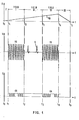
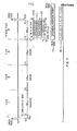
- the three coordinate information for each signal period is shown one above the other as x (t), y (t), z (t) depending on the time t.
- Each course of coordinates is divided into time sections I ', I, II, III, IV (indicated by ordinates and dash-dotted lines at the times t o , t 1 , t 21 t 31 t 4 , t 5 ).
- Section I ' serves to transmit a y-configuration word, which will be described in more detail later, following the triggering of an x-deflection.
- Section IV is the return phase (retrace time) of the z deflection of an electron beam of an x, y, z oscilloscope in the respective device, which will also be explained later.
- Sections I, II, II are the main sections for recording alphanumeric characters and analog signals. In the following, they are also referred to as fields for analog or character display.
- the z-deflection begins with the ramp voltage X R at time t.
- a fast y raster Y R follows at time t 1 .
- This grid is the basis for a character representation.
- the two quantities x and y in field I as ramp voltages are system-inherent constant quantities that can be generated in the device itself. An independent transmission of such grids to the individual device via a common signal line (signal bus) is therefore unnecessary. Only the trigger signals required for triggering the ramp voltages X R and Y R need to be passed on in the form of an x synchronizing signal or a y configuration signal. The presence of two system-constant coordinates x, y in field I can, however, be used to transmit address signals for a character generator located in the respective device via a common signal line (signal bus).
- the character generator forms in the respective controlled device Bright tactile signals, which are assembled in synchronism with the rapid y-character grid generated simultaneously in the device on the screen of an x, y, z oscilloscope to form the desired alphanumeric characters.
- the address signals for the character generator to be transmitted in the information section I are indicated in FIG. 1 for the coordinate z as digital signals CA (Character Addresses).
- section I A significant property of section I (field I) is that the coordinates x and y are inherently constant, while the coordinate z is foreign to the system and variable. However, since two coordinate sizes are constant sizes, the third variable size z can be transmitted to the respective device via the common signal line.
- the situation in information section II (or field II) of the diagram in FIG. 1 changes.
- the y coordinate as a transmission section of an analog signal A (e.g. EKG) is now external and variable.
- the coordinate y in the case of field II is not an inherent constant quantity;
- the z coordinate must be system-specific and constant in addition to the x coordinate in field II. This is also the case because, according to the diagram in FIG. 1, the z coordinate in the information section II shows a constant voltage curve.
- FIG. 1 The illustration in FIG. 1 is only an example. It goes without saying that the individual fields I to III can be strung together as desired. The number of all fields can be specified differently from three. Analog signals can be displayed together with characters in different fields. However, only analog signals or only characters can be mapped in a single track. As already indicated at the beginning, section I 'preceding the main fields I to III can only be used for the transmission of a y configuration signal. It goes without saying that, in addition to the configuration signal in this section, other arbitrarily designed command signals can also be transmitted. Such additional signals can, however, as already indicated at the beginning, also be placed in the phase (eg fields I and / or III) in which rapid y-rasters are generated for the representation of the characters.
- phase eg fields I and / or III
- additional command signals are then transmitted together with the digital address signals CA in a suitably mixed form via the common signal path.
- additional signals can also be used in phase IV, i.e. that is, in the return phase of the electron beam after an x deflection.
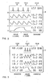
- FIGS. 2 and 3 show analog signals and characters to form an overall image on the screen of an x, y, z oscilloscope.
- the screen of the oscilloscope is designated by B.
- field I on screen B shows alphanumeric characters.
- Sections of an analog signal A are recorded in field II.
- Figure 2 the recording of this analog signal is continued in field III.
- FIG. 3 alphanumeric characters in the form of limits are again shown in field III.
- the beam deflection of the electron beam for signal recording takes place in a top view of the screen B from right to left.
- the alphanumeric characters always appear in field I first. This is followed by field II with the representation of an analog signal.
- Field III can then either be used to continue recording the analog signal (FIG. 2) or to re-display alphanumeric characters (FIG. 3).
- the oscilloscopes shown are, for example, four-channel oscilloscopes. These oscilloscopes thus work in such a way that a total of up to four different analog signals with correspondingly assigned characters can be represented in chronological succession in channels which are layered one below the other.
- one or more characters e.g. up to two characters as shown
- the present embodiments of the Figures 2 and 3 are on the screen of the respective four-channel oscilloscope in channel 1 z.
- B. the patient's ECG is shown together with characters, which characters for both figures in column I z.
- the analog signals to be recorded can therefore be assigned in the visual image either only pure size information or, in addition to the pure size information, also limit information about maximum or minimum permissible limit values of the physiological measurement signals in the form of alphanumeric characters.
- limit value information By adding limit value information, limit violations and thus critical developments of a physiological measured variable can be recognized immediately.
- Critical limit violations are also indicated in the present case by issuing an appropriate alarm signal (in particular acoustic and / or optical in nature). If the image content of a trend memory is shown in the basic device, the analog curves shown in FIGS. 2 and 3 are correspondingly replaced by trend curves.
- the image of all signals to be imaged is flicker-free.
- the total time of beam deflection on the screen of the respective oscilloscope is therefore 20 ms. If recording in four channels is desired, the total deflection time including the return per channel may not exceed 5 ms.
- FIG. 4 shows a time schedule adapted for this purpose for signal transmission.
- This time period T is subdivided into a total of five time periods I ', I, II, III, IV.
- a synchronization pulse SP (3 volts, 3 microseconds) is set at the beginning, which, e.g. B, determines the start of an x-deflection with its trailing edge at time t.
- the control of all affected devices by the synchronization pulse is such that the synchronization pulse of a single device that occurs first synchronizes the x-deflection of all other devices with one another, unless a synchronization pulse is pressed on all other devices from the outset by an external center .
- the synchronizing pulse SP is followed first by the time interval I ', which in the present case is 80 ⁇ s long.
- a deflection configuration signal (8-bit sweep configuration word) is transmitted to all devices to be controlled in the device configuration as a digital signal, which serves as an indication signal for such as start and / or the end and the type and location of the current y representation on the screen of an oscilloscope that is just switched on in comparison with the signal representation to be transmitted from another device.
- the deflection configuration signal can be defined as an 8 bit word in levels BIT 0 to BIT 7 for the present exemplary embodiment when used on a four-channel oscilloscope as follows:
- the first field I follows section I '.
- the duration of this field is 1,280 ⁇ s.
- field II is followed by field II, which is again 1,280 microseconds long.
- Field III is connected to field II at time t 3 and also lasts 1,280 ⁇ s.
- the x-deflection is then completed by section IV, which is 960 ps long and which defines the return time for the electron beam.
- the returned electron beam is faded in by a special selection in the configuration word as a thin track R in the image recording.
- the return track R signals the course of the zero line in each channel.
- the feedback phase IV for the electron beam can be used to transmit any additional command signals. Cyclically circulating storage values of the analog signals can just as well be the oldest from the image repetition memory during the retrace time Values are removed and, for example, fed to a running recorder, recorder or the like as so-called delayed data.
- phase IV data can be rearranged in memory in any way, or permanently deleted.
- the end of Retrace Phase IV is also the beginning of a new distraction period.
- the triggering always takes place in such a way that the electron beam of the oscilloscope, regardless of where it is in the reverse phase at the moment on the screen, is immediately withdrawn to its starting position in the right outer edge position of the screen.
- the instantaneous instability resulting from the abrupt interruption of the feedback phase is bridged by the time interval I 'following the synchronizing pulse with the transmission of a y configuration signal, which is itself not shown on the screen.
- the invention is used in particular in the medical field when taking physiological signals, such as in particular EKG, blood pressure, temperature C0 2 etc. on the patient's body.
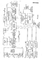
- a single device of this type is shown in the basic circuit diagram in FIG. 5, for example.
- This device comprises a total of four plug-in modules 1 to 4 for receiving and forwarding the physiological signals received to a module / coupling and control unit 5.
- This unit 5 is with each individual plug-in module 1 to 4 in terms of energy via a pair of energy coupling coils 6 and 7 for transmission of the Operation of the plug-in modules required th energy from unit 5 to module 1 to 4 coupled.
- the transmission of the physiological signals or other received signals from a plug-in module to the unit 5 takes place by means of optocouplers 8, 9.
- a transmitter diode in particular a luminescent diode for infrared light.
- the number 7 indicates a light receiver, in particular a photodiode.
- another optocoupler 10, 11 is available for the transmission of signals, e.g. B. switching signals, A / D clock signals or other control signals from the unit 5 to a plug-in module 1 to 4, another optocoupler 10, 11 is available.
- this optocoupler there is a transmitting diode 10 on the unit 5 and a receiving photodiode on the respective module 1 to 4. Further details on the internal basic circuit structure of a module 1 to 4 and the module / coupling and control unit 5 can be found in the description below 13 to 15 can be seen.
- the device in the device housing has an indentation into which the slide-in modules 1 to 4 can be inserted one above the other on levels.
- the indentation comprises a rear wall on which the unit 5 with the first half parts of the respective energy coupling point or the respective optocoupler are mounted.
- the other half of the energy coupling point or the respective optocoupler is, as indicated in FIG. 5, arranged on the rear of the respective plug-in module 1 to 4. If the plug-in module is pushed into its end position in the indentation of the device housing, the half parts carried by it join each coupling point with the half parts of the rear wall to form a complete galvanically isolating coupling point for energy and signal transmission. The unit is ready for use.
- the physiological or other signals picked up by the unit 5 are now fed via the data arrow 12 to a microprocessor 13 for data processing (preprocessor), in particular data scaling and data weighting.
- the microprocessor 13 for preprocessing can also transmit signal data, such as clock signals, configuration signals or the like, according to data arrow 18 transmit the unit 5 with the signal path switched on via the optocouplers 10, 11 to the individual plug-in modules 1 to 4.
- the memory 15 is normally permanently assigned to the central microprocessor 14 (data arrow 19).
- the preprocessing microprocessor 13, however, is switched off. Only when the preprocessing processor (line 20) requests DMA does the central microprocessor 14 ′ separate from the memory 15 and the preprocessing processor 13 takes control of the memory (data arrow 21).
- the central microprocessor 14 is the heart of the device. From it, the signal data is read via a data line 22 via a central shift register 23 into a dynamic RAM memory 24 under the control of an address computer 25 which receives address data from the central microprocessor 14 via an address line 26.
- the central shift register 23 takes over all accumulating data in parallel formation and reads them out serially.
- the clock sequence for reading in and reading out data is specified by a central clock generator 27.
- the data to be forwarded from the RAM memory 24 to the oscilloscope 28 for recording are preprocessed in a processing device 29 and then transferred to the oscilloscope.
- the device 29 contains all the components that are necessary for generating or for forwarding the signal sequence according to the invention (composite video signal) according to FIG. 1.
- signals and characters corresponding to FIGS. 1 to 4 are processed and sent to the device's own monitor 28.
- all signals processed in this way are also sent via an output 30 (composite video output) to a transmission line (composite video bus) common to all devices of any device configuration.
- the device 29 also includes a corresponding input 31 (composite video input) via which the device can also be connected to the common connecting line for all devices. From there, composite video signals from the common transmission path can be taken over from the common transmission path for recording on the device's own oscilloscope 28, if necessary, for example in the event of an alarm, by switching off the own data flow to the oscilloscope, from any other device, in particular that of the alarm case.
- the alarm is generated by an alarm transmitter 32 connected to the central microprocessor 1 4 and z. B, in the direction of arrow 33 on an alarm bus.
- a keypad 34 is used to enter special command data into the central processor 14, e.g. B. on the front panel of the respective device, with sensor 35 for the correct input.
- An LED display 36 (light-emitting diodes) with driver stage 37 is used to display data entered or data generated during signal processing.
- a loudspeaker 38 with amplifier 39 is used for acoustic signal display, e.g. B, for alarm, for key clicks on the keys of a keypad or clock for occurring QRS pulses or display for interrupted program execution of the central processor.
- Component 40 is an additional ROM and RAM memory for the central microprocessor.
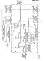
- the device for generating and forwarding or receiving composite video signals is part of z. B, a device according to FIG. 5 is shown in detail in the basic circuit diagram of FIG. 6. Accordingly, the output of the central shift register 23 bifurcates in the direction of the signal processing device 29 in at least three signal paths 41, 42 and 43. A special signal processing element is switched on in each of these signal paths. There is a decoder 44 for the y configuration word in the signal path 41. In the signal path 42, however, are the character generator 45 for character formation (local ROM for 2 x 7 character display in 8 bit code) and the ramp generator 46 for generating the fast y deflection pattern (y ramp voltage Y R ).
- the digital-to-analog converter 47 for regenerating the analog signals A is switched on in the signal path 43.
- the outputs of the decoder 44 for the y configuration signal, the generator 46 for the y deflection grid and the digital-to-analog converter 47 lead to a device 48 for processing all incoming signals for the vertical deflection signal y for the downstream oscilloscope 28.
- the character generator 45 goes with a further output to the light sensing device 49 of the oscilloscope, which supplies the light sensing pulses necessary for the character structure.
- the signal path described is the path for the composite video signal as the device itself generated.
- an additional device output 30 composite video output
- This additional signal path is identified in FIG. 6 by taps 51, 52, 53.
- the taps 51 and 52 are located on the signal paths 41 and 42 in front of switches 54 and 55, which are connected upstream of the decoder 44 for the y configuration signal and the character generator 45.
- the tap 53 on the signal path 43 is located at the output of the digital-to-analog converter 47 before a switch 56.
- the switches 54 to 56 normally connect the signal paths 41, 42 and 43 directly to the system-specific image generators 44 to 49.
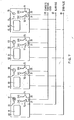
- FIG. 7 shows a typical application of the invention to a chain connection on individual monitoring devices without its own control center.
- a total of four bedside devices 60 to 63 are shown, each of which is constructed in such a way and generates such a composite video signal as is shown in FIGS Explanations to the previous Figures 5 and 6 was described.
- All four devices in this device chain (the number of devices can be increased as required) are connected to each other via a total of three lines 64, 65, 66 connected (or interconnectable via switches, as will be explained in more detail below).
- So z. B. the line 64 of the common signal bus (CVB) for the composite video signal (CV).
- CVB common signal bus
- Line 65 is the common alarm bus and line 66 is finally the common transmission line for the synchronizing pulse SP for synchronizing the x-deflection of all devices 60 to 63.
- Each of the devices has an LED button 67 on the front (indicated schematically) to 70.
- a light emitting diode is therefore integrated in each of these buttons.
- Each of these light-emitting diodes is in turn connected in terms of circuitry to the alarm bus 65 in such a way that it lights up within the key when an alarm signal is generated by another device in the chain and is output on the alarm bus.
- the LED there is not activated in the alarm device itself.
- the alarm situation is visually and acoustically displayed with separate display means. The doctor or the supervising nurse can then immediately distinguish whether the device in question gives an alarm itself, i.e. whether the patient connected to it is itself the alarm patient or whether another device in the chain with the patient connected there is the subject of the alarm.
- switches 71 to 78 are arranged in lines 30 (see FIGS. 5 and 6) of the video signal outputs (CVO) of the devices.
- Switches 75 to 78 are in lines 31 (see FIGS. 5 and 5) and 6) the Video Signal Inputs (CVI).
- a closed CVO switch 71 to 74 means that the device in question 60, 61, 62 or 63 specifically its composite video signal, which it also displays at the same time on the screen of its own oscilloscope 79, 80, 81 or 82, in feeds the composite video bus 64.
- a closed CVI switch 75 to 78 means that the composite video signal that is currently being fed into the composite video bus 65 from another device is taken from the device in question via the video signal input from the CV bus and on the screen of the oscilloscope 79, 80, 81 or 82 of this device instead of displaying your own composite video signal.
- the device 63 alarm.
- This alarm is communicated to devices 60, '61 and 62 (or all other devices if they are also connected in the chain) via alarm bus 65.
- the LED buttons 67, 68 and 70 of these devices thus light up, which is indicated in FIG. 7 by symbolic light rays on the edge of the buttons.
- the CVO switch 7 4 of the device 63 has also been closed at the time of the alarm.
- the CVO switches 71, 72 and 73 of the devices 60, 61 and 63 remain open, since no alarm was generated in these devices. Accordingly, the composite video signal of the alarm device 63 is fed into the composite video bus 64.
- This composite video signal can now be taken from any device 60 to 63 by pressing the LED button 67 to 69 from the CVB 64. Pressing a lit LED button causes the steady light to flash. This indicates that the oscilloscope of the device in question is no longer displaying its own signal, but an external signal. A key will blink in Figure 7 symbolically indicated by rays that run radially into the key center.
- the LED button 67 of the device 60 is pressed.
- the CVI switch 75 of this device was accordingly closed and the CV of the alarm device 63 thus reaches the CV-processing signal part of this device via the composite video input of the device 60 and from this accordingly to the screen of the oscilloscope 79.
- the respective COI switch 75, 76, 77 or 78 can symbolize the three changeover switches 54, 55, 56.
- An open COI switch in FIG. 7 would correspond to the first switch position of the switches 54, 55, 56 in FIG. 6, in which the device-specific CV generators 23, 24 etc. via lines 41, 42, 43 directly with the image-building blocks 44 to 49 are connected.
- a closed COI switch of Figure 7 would exist hinge ', the second shift position gen again, in the interrupted direct these compounds and for the image-building blocks are (except for the A / D converter 47) connected to the signal lines 57, 58, 59 of the CVI.
- the respective COI switch can, however. B.
- the COI switch can also be designed as an additional control switch for the switches 54, 55, 56, which switches the switches 54, 55, 56 as soon as it is closed by pressing the LED button.
- the COI switch can also be an integral switch contact part of the LED button.
- a significant property of a derailleur circuit is that each device within the chain can take over the function of a central device, which then functions as a central device So from any other device that z. B, just generated alarm, whose composite video signal can be called up for recording on the screen of your own oscilloscope. It is only essential that an LED button is pressed on the corresponding device to take over the central function.
- FIG. 8 An arrangement of bedside devices, on the other hand, works according to a somewhat modified principle, for which a central unit is provided from the outset to control the overall process.
- a central unit 83 is assigned a total of n individual devices (bedside units) which are connected to the central unit in a star configuration via composite video buses on the device side for composite video signals CVB 1 to CVB n and alarm buses for device-side alarms AL1 to AL n.
- a single central composite video bus (composite video central) for a central composite video signal CVC leads back from the control center to the bedside devices.
- each of the bedside devices of the star formation with a center is constructed in exactly the same way and it functions in terms of generating its CVB 1 to CVB n in exactly the same way as was described for FIGS.
- Blocks 86 and 87 within the device blocks 84 and 85 thus essentially symbolize the summaries of those components 41 to 56 of the image processing and image recording part of the devices, as are detailed in particular in FIG. 6.
- the blocks 88 and 89 indicate the image repetition memory 24 with the associated shift register 23, address computer 25, clock generator 27, etc., as these components are also explained in principle in FIG. 6.
- the central office itself is what the central image processing and image construction part 96, in principle constructed in exactly the same way as a bedside device.
- a bedside device Corresponding to a bedside device, it also includes a repetition memory 97 and a central microprocessor 98.
- a central signal and data multiplexer 99, an alarm multiplexer 100 and a control device 101 for data are located in the control center on suitable supplementary cards - and address control inserted between central multiplexer 99 and central image repetition memory 97.
- the central signal and data multiplexer 99 has the input lines 90, 91 etc. to 92 for a total of sixteen composite video signals CVB 1 to CVB 16 of the sixteen individual bedside devices.
- a further output line 111 of the central multiplexer 99 leads via a switch 112 directly to the signal input of the image processing and image recording part 96 of the control center. Via this switching line, the image part 96 of the control center receives the complete composite video signal CVB of an arbitrarily selectable bedside device of the star configuration.
- the central multiplexer 99 also has three outputs 113, 114 and 115 for recorder signals REC 1, REC 2, REC 3, which, if required, can be registered on two signal repeaters 116, 117 integrated in the center and an externally connected signal recorder (connecting arrow 118) .
- Synchronization signals Synch 1, Synch 2, Synch 3 are used to synchronize the recorders, which are applied to the output lines 119, 120 and 121 of the central multiplexer 99.
- the signals REC1, REC 2, REC 3 are together with the synchronizing signals Synch 1, Synch 2, Synch 3 decoded in decoders 122, 123, 124 and then connected to the recorders by means of switches 125, 126, 127.
- the alarm multiplexer 100 has an output alarm bus 128 to the central processor 98.
- the central processor 98 is connected to the image part 96 of the control center via a data and address line 129 and is also in constant communication with the control device 101 via lines 130, 131.
- very essential component is the central composite video bus 132.
- the composite video signal CVC of the center is fed back to the bedside devices (or also in the direction of the recorders 116, 117 etc.) via this central bus. If required (again by pressing an LED button as in the case of a chain connection according to FIG. 7), the central composite video signal can be called up at any time from the central bus 132 into a bedside device. To do this, a switch 133, 134 etc. (LED button) only has to be flipped again.
- the CVC then reaches the image processing section via the composite video input of the device in question.
- the own signal image is then replaced by the central image.
- a significant property of the star configuration is therefore that the composite video signals CVB 1 to CVB n of the bedside devices 84, 85 etc. are guided in a star shape to the control center 83.
- the center also comprises only a single oscilloscope with a maximum of four channels. This means that at most the four channels of a single display device 86 or 87 etc. can be taken over as a selected CVB via line 111 on the screen of the central oscilloscope.
- a time-graded switchover of the central display device 96 to other display devices is indeed possible by the time multiplexing of the multiplexer 91 and is also carried out in this way; However, it is difficult to carry out an imaging process which signals of certain channels from image devices 86, 87 etc.
- the trick described thus makes it possible for a central oscilloscope within the central unit 83, e.g. has four channels, a total of four different channels from oscilloscopes from four different bedside devices can be displayed in any order.
- the central processor 98 now controls the signal transfer between the image repetition memory 97 and the display device 96 in such a way that the delayed values of the alarming signal track (e.g. alarming EKG) instead of a previous signal value recording in the channel with the highest number, i.e. in the fourth channel. If a second alarm signaling track occurs, it is correspondingly written into the next lower channel, i.e., the third channel, etc. Simultaneously with the display of the alarm signal track, the image repetition memory dub the number of the bed on which the alarm device is located. The bed number is highlighted on the central screen by flashing, so that the person monitoring at the control center immediately recognizes that there is an alarm on a bedside device with a specific bed number.
- the alarming signal track e.g. alarming EKG
- the alarm can be sent from the control center 83 via the control center Bus 132 can also be communicated to other non-alarming bedside devices.
- z. B again an LED button according to the description above.
- the central composite video signal CVC can then be adopted on the screen of the oscilloscope of the device in question by switching off the own image display.
- FIG. 9 shows in a detailed representation the inner basic structure of the multiplexer 99, as was already explained in connection with the structure and mode of operation in connection with the star connection of FIG. 8.
- the distribution of the various signals in multiplex operation on the different output lines is carried out by conventional analog switches 135 to 146 inside the multiplexer.
- FIG. 10 shows the internal structure of the control device 101 according to FIG. 8 in the connection between multiplexer 99 on the one hand and image repetition memory 97 and central processor 98 on the other hand.
- the control device comprises four individual blocks 147 to 150, each of which, in principle, is internally constructed as shown for block 147 in detail.
- Each of the blocks 147 to 150 thus comprises a shift register 151 for data words (data word shift register), a counter 152 (strobe counter) for clocking the shift register, which includes a clock input 153, a synchronizer 154 (synchronizer) for the count clock and a word counter 155 for the addresses.
- the output data of the data shift register 151 go via an output 156 to the data buses 107, 108 for image repetition memory 97 and central processor 98.
- the output addresses of the word counter 155 accordingly go via an off aisle 157 to address buses 109, 110 for refresh memory and central processor.
- the control device 101 also includes a shift register 158 for data words with output 159 to the data buses 107, 108 and a word counter 160 with output 161 to the address buses 109, 110 for the forwarding of character addresses CH.
- the block 162 again comprises a synchronization and control device (four cycle synchronization and control) with start input 163 for starting the reading of a character (start character read) and input 164 for the timing which controls the image construction of the character (timing from display control, see again here Figure 6 in connection with Figure 5).
- An output 165 leads to a control unit 166 (DMA Control Arbitrator and Multiplexer Control) which is in communication with the central processor via lines 130 and 131.
- DMA Control Arbitrator and Multiplexer Control DMA Control Arbitrator and Multiplexer Control
- delayed data are used to mix signal traces, which occur in the respective retrace times of the x-deflection.
- the duration of this feedback phase is 960 N s, which is again demonstrated in FIG. 11 in memory of FIG. 4.
- a pulse plan is drawn in below the time diagram already described, which purely schematically deals with the data transmission in field IV during the feedback phase of the x-deflection. The data transmission takes place in digital form.
- the state ZERO (0) is also due to the occurrence of the voltage level + 0.75V and the state ONE ("1") due to the occurrence of the digital signals of the retrace time IV Voltage levels - 1V occupied in the composite video signal.
- the feedback phase IV can now be up to ten digital words are transmitted, each of which has 8 bits.
- a NULL (0") is transmitted, except for the times when digital words are transmitted.
- the composite video signal is at the + 0.75V level.
- the transmission of digital words begins approximately 50 ⁇ s after the start of the feedback phase.
- Each word to be transmitted is opened with a start bit 167, which is 2 ⁇ s long and which signals a ONE ("1").
- This start bit is then followed by a word 1 68, which consists of 8 bits 169 to 176, each of which is also 2 ⁇ s long.
- the individual bits 169 to 176 can have ZERO or ONE status, depending on the content of the word: In FIG. 11 these alternating options between ZERO and ONE are indicated schematically by two diagonals in each bit.
- the first bit is identified with LSB and the last bit with MSB.
- LSB stands for "Least Significant Bit” and MSB for "Most Significant Bit”. This defines the direction for each word in which the bits of this word are to be read.
- the first word of such a sequence that is always transmitted is an index word.
- This index word which is shown in detail in FIG. 11 in the lowest representation under the code number 178 broken down into its 8 bits, provides information about flow variables for the recording, such as. B, via recording speed (speed), the channel selection (channel CHAN 1 to CHAN 4 or CHAN 1 'to CHAN 4 '), the presence or absence of trend values (trend points), the presence of current and / or delayed measured values (real time data, delayed data) etc.
- the first four words following the index word define delayed signal values for the four channels CHAN 1, CHAN 2, CHAN 3 and CHAN 4 and are also entered in the term 177 in this name.
- the 8-bit index word is composed, for example, as follows:
- This BIT determines whether there is a trend word for the next channel.
- a trend word is only transmitted if the transmission has been requested.
- This request can come from a recorder associated with the bedside device. However, it can also come via UART through a central recorder of the central station (see again description of FIG. 5).
- FIG. 12 shows the basic mechanical structure of an electromedical monitoring device with four slots modules, as is preferably used in connection with the invention as a bedside device.
- the device comprises a device housing 179 with the front surface 1 80.
- On the right side of the front surface is indicated an opening for a recess in the interior of the device housing with the 181st Through this opening 181, a total of four plug-in modules can be inserted into the recess, which are again numbered 1, 2, 3 and 4 in accordance with the basic circuit diagram of FIG. 5.
- the device is equipped with an x, y, z oscilloscope, the screen of which is indicated at 182.
- the elements 184, 185 on the front panel are operating and display elements, such as key switches, LED display fields, etc. Their arrangement is shown purely schematically.
- Element 186 indicates the previously described LED light button for displaying and accepting the external alarm.
- Element 187 identifies e.g. B. the reset button for an alarm in your own device.
- the device shown in FIG. 12 is again an electromedical device.
- the plug-in modules 1 to 4 are therefore part of the signal transmission system for physiological signals which are removed from the body of a patient by means of suitable pickups.
- customers (not shown) are positioned on the patient's body and coupled to the respective insert via a signal cable (also not shown).
- the plug-in modules thus comprise plug-in sockets 188 to 191 for corresponding plugs of the signal cables.
- the remaining elements 192 to 195 are again only purely schematic indications of data keys or LED display fields of the plug-in modules.
- the bottom shelf 4 is, for example, a C0 2 shelf, the two middle shelves are e.g. B.
- slots for blood pressure and temperature measurement and the upper slot 1 serves z. B for EKG measurement.
- the device shown can be used together with other similar devices to a chain with structure and operation, as shown in Figure 7, are interconnected.
- the device described can just as well be combined with a corresponding number of further devices together with a control center to form a star connection, as shown in FIG.
- the order in which the individual plug-in modules 1 to 4 are arranged in the device in FIG. 12 is completely arbitrary.
- FIG. 13 shows in the basic circuit diagram the essential internal structure of an EKG insert with three channels 1H, 1A, 1B.
- Channel 1H is a top speed channel; this channel, which is only in the ECG slot, is scanned 2400 times a second.
- Channel 1A is the main data channel for the ECG. This channel 1A is scanned a total of 400 times a second. Channel 1B can serve as a second data channel for a further measured variable. This channel is scanned only 200 nal per second. In principle, what has been said for channels 1A and 1B also applies accordingly to the remaining three plug-in modules 2 to 4. Corresponding channels 2A, 3A and 4A or 2B, 3B and 4B are present in these plug-in modules.
- all four plug-in modules in terms of channels A and B, have the same structure. According to the illustration in FIG. 13, they therefore all comprise the signal inputs E11 and E12.
- a preamplifier 197 and 198 follow each of these signal inputs.
- Each of the preamplifiers has a control input 199 or 200, at which the degree of amplification can be regulated by a control signal.
- the setting can be made using bit combinations, together with a configuration word for the conversion to the signal processing part on the device side to the respective module.
- state detectors 205 and 206 at outputs 207 and 208 by respective bit signals report the j e or oversized condition in which the module in the respective channel is located.
- the status indicators 205 and 206 include in a known manner, for. B, those measuring elements which determine whether the pickups for the individual signals are correctly positioned on the patient's body and whether the signal reception and transmission in the channels themselves is in order. These data are together with identification signals for the respective module and z. B. also together with other data, which was entered, for example, via a keypad of a module, as a so-called auxiliary word from the module in the direction of the processing part of the device.
- the keypad of a module is indicated schematically with the number 211.
- An 8-bit shift register 212 is used to transmit the auxiliary word, which accepts auxiliary data from the signal transmitters 205 and 206 and, if appropriate, from the keypad 211 at four inputs 213 each with 1 bit.
- the four bits of the remaining four inputs 214 of the shift register 212 formulate the identification signal for the respective module. These four inputs 214 for the identification signal are thus wired differently for each module in a corresponding modification.
- the auxiliary word (auxiliary word) of the shift register 212 of each plug-in module is transmitted together with the digital measurement data of the analog-digital converter 196 via the transmitter diode 8 to the associated photo receiver 9 in the signal processing part of the device.
- the Signal sequence from digital data, which is therefore sent from the respective module 1 to 4 into the device, is shown in FIG. 15 below.
- the pulses D1 to D14 are the digital measurement data of the analog-digital converter 196.
- the eight pulses A1 to A8 stored in between are the auxiliary data; they form the auxiliary word and contain the identification signals for the identification of the respective sending module.
- the pulse sequence which is transmitted from a respective light transmitter 10 on the side of the device to a light receiver 11 on the side of the respective module 1 to 4 and which specifies the conversion clock for the respective analog-digital converter 196, is shown in FIG. 15 above indicated.
- This pulse sequence comprises a total of fourteen pulses CL1 to CL14 per conversion cycle.
- the interposed pulses CC1 to CC8 are each 8 bits, which serve as a configuration word for setting the filters and amplifiers based on commands that are transmitted from the device side. These commands can be generated by the respective microprocessor on the device side itself. However, it can also be such commands that z. B.
- each cycle of conversion pulses also includes corresponding pulses of a configuration word, with the help of which commands can be executed in the respective slot.
- each conversion cycle includes a total of fourteen clock pulses for appropriately fourteen conversions at the analog-to-digital converter 196.
- the clock pulses are each 2 microseconds long and their distance to each other - is of 12 microseconds.
- a last pulse AZ follows in every cycle at intervals of 24 microseconds on the fourteenth clock pulse CL14.
- This pulse AZ is a so-called auto zero pulse, which automatically sets the analog-digital converter 196 to ZERO via a pulse shaping element 215 (eg monoflop). If one takes into account that the first clock pulse CL1 is only generated 12.5 microseconds after the start of a cycle and the respective cycle is only completed 12 microseconds after the AZ pulse has occurred, the total duration of a cycle is 204.5 microseconds. A further 12.5 microseconds after the end of a cycle then begins a new cycle, as is also indicated schematically in the pulse diagram in FIG.
- the clock pulses CL1 to CL14 for the conversion clock go directly to the analog-digital converter 196.
- the eight pulses CC1 to CC8 of the configuration word are written into an 8-bit shift register 216.
- the conversion cycle of the previous cycle is still running during the period of writing the respective word of a cycle into the shift register 216.
- the conversion word of the previous cycle is located in an 8-bit shift register 217.
- Each configuration word stored in the shift register 216 is taken over in parallel by the second shift register 217 when the last pulse CC8 is received.
- the configuration word for the next cycle is thus available at the output of the second shift register 217.
- the analog-to-digital converter 196 shown in FIG. 13 can in principle be constructed as described in US Pat. No. 3,588,881.
- the link 223 between the sampling switches 209, 210, 221 and the analog-digital converter 196 is a common sample and hold link.
- At the The output of the analog-digital converter 196 is a pulse mixer 223a.
- FIG. 14 shows the basic internal circuit structure of the control and coupling board 5, as opposed to the slots for signal and energy coupling on the side of the device.
- the preprocessing microprocessor preprocessor
- the arrow 21 leads in the direction of the main memory 15 (shared memory).
- the basic clock for the pulses of a conversion cycle is supplied by a clock generator 224 (counter) which is synchronized by the preprocessing processor 13.
- the pulses of the clock generator go into a control unit 225.
- the above-described clock cycle 1H, 1A, 1H, 2A, etc. runs via corresponding pulse switches.
- Each clock pulse for 1H goes to a clock line 226 and to a clock line 227.
- the clock pulse of the line 226 clocks a shift register of an arrhythmia addition.
- the same clock pulse controls a switch 229 via line 228 to the switch position shown.
- a switch 230 is closed and a switch 232 is opened via an inverter 231.
- a request signal for a recirculation register 234 (recirculation register for high speed) is also generated via a control line 233, in which conversion pulses 1H are constantly in circulation.
- the polling signal causes a pulse 1H to be output at the output 235 of the circulation register 234.
- the pulse 1H passes through the switch 230, which is closed at this time, to a superimposition stage 236, which passes it via the switch 228 to the line 237 and from there via the line 238 to the transmission diode 10 of the transmission channel for the uppermost plug-in module 1 forwards.
- the transmitter diode 10 sends the pulse 1H in the direction of the photoreceiver 11 in the module 1, which then forwards it as a 1H pulse on the one hand to the analog-to-digital converter 196 and on the other hand to the formation of the shift registers 216, 217.
- the pulse 1H also opens a switch 239.
- the superimposition stage 236 is a pulse mixing stage in which the remaining pulse pulses for the channels 1A to 4A and 1B to 4B are mixed in via the line 244 in the predetermined sequence. Finally, the eight pulses CC1 to CC8 of the configuration word, which is to be retransmitted to the respective module, are also added to these pulses via a line 245. The admixture takes place in each case via the closed switch 232. The pulse sequence thus mixed is fed to a multiplexer 246 via the switch 228, which is controlled outside the clocks 1H into the dashed position. This multiplexer then, controlled by the preprocessing processor 13, clocks the transmit diodes 10 via lines 246a, 246b, 246c and 246d.
- light pulses are transmitted in accordance with the desired clock sequence to the photo receivers 11 on the side of the plug-in modules 1 to 4, from where they then finally arrive as a conversion clock at the analog-digital converters 196 or as a configuration word to the shift registers 216, 217.
- the high-speed channel for the 1H scanning is permanently assigned to an insert in the uppermost position.
- relatively high-frequency events occur at most in connection with the EKG measurement. This means that a high speed signal is practically only received when the EKG module is inserted in the first position. If, however, there is a slot for low-frequency signals in this position, the high-speed scanning 1H runs empty. If high-speed scanning is required, the ECG module must be inserted in position 1. However, all other positions can be freely selected.
- the device receives from the respective module 1 to 4 measured values D1 to D14 together with an auxiliary word A1 to A8.
- This auxiliary word also contains the identification signal for the respective plug-in module.
- all the pulses received by the photoreceivers 9 on the side of the device are now transferred to a pulse line 246c, from where they reach the line 247 via the switch 239, which is always closed when such pulses occur. From there, on the one hand, they are passed on to the input of a first 8-bit shift register 248. On the other hand, they also reach the input of a second 8-bit shift register 250 via a line 249. Pulses which leave the second shift register 250 in overflow are clocked into a third shift register 252 via a line 251, which, in principle, is also an 8-bit Shift register is, however, only takes over 6 bit data.
- the shift registers 248, 250 and 252 are clocked by the control unit via clock lines 253, 254 and 255.
- the shift registers 250 and 252 run in push-pull to the shift register 248, which is controlled by an inverter 254 becomes.
- Lines 256, 257 and 258 are enable control lines for the respective shift register.
- the push-pull on the shift register 248 has the result that only that data of the pulse sequence that arises that is generated during pauses in the measured value data D1 to D14 is written by this register. However, such data are data A1 to A8 of the auxiliary word.
- the 8-bit shift register 248 thus acquires the data of the auxiliary word.
- the second 8-bit shift register 250 which operates in push-pull mode, on the other hand clocks measured value data. As soon as the first eight individual data have arisen, there is an overflow to shift register 252. At the end of each conversion cycle, 8-bit shift register 248 thus contains the auxiliary word, while in 8-bit register 250 the measurement data D14 to D7 and in register 252 measurement data D6 to D1 are saved.
- the stored data can now be transferred in groups to the preprocessing processor by means of latches 259, 260 and 261. From there they can be sent to the main memory and left to the main processor for further processing.
- the buffer memory 261 and the shift register 252 also serve to transfer the configuration word from the preprocessor 13 to the line 245 at times when no measurement data are currently being stored in the shift register 252.
- FIG. 16 shows the interplay between preprocessor (preprocessor), main memory (shared memory) and central microprocessor (central processor) of a device according to FIG. 5 in a detailed block diagram.
- the preprocessor 13 is not DMA-capable.
- the central microprocessor 14, is DMA-capable, ie this processor has a fixed access order to the main memory 15 Circuit trick, the preprocessing microprocessor 13, which is not DMA-capable per se, is prepared in such a way that it becomes DMA-capable.
- the trick is as follows:.
- the preprocessor 13 issues a DMA request to the main processor 16 at certain time intervals. This is done in such a way that a specific address appears at the output of the preprocessing processor 13. In the present embodiment of Figure 16, this address z. B, from three binary ones.
- This address reaches a decoder 264 via an address line 263.
- This decoder 264 recognizes the selected address whenever it occurs. It then generates a DMA pulse at its output 265.
- This pulse now reaches the central microprocessor 14 via a first branch line 266. At the same time, it is applied to a clock delay element 268 via a second branch line 267.
- the DMA pulse arriving at the central microprocessor 14 triggers a DMA request there.
- the central processor 14 thus only completes those operations which it had started before the arrival of the DMA request and had not yet completed.
- the central microprocessor is therefore not switched off immediately when a DMA request is received; A certain time elapses before the switch-off (all output buffers of the central processor take up a high-resistance value). During this period, during which the central processor 14 is still in communication with the main memory 15, it must be ensured that the preprocessing microprocessor 13 remains switched off from access to the main memory 15.
- This clock delay element is a frequency reducer, which reduces the clock frequency with which the preprocessing processor 13 is clocked in the normal state to a value which is much lower than the normal value.
- the normal value of the clock frequency is approximately 4 MHz, which corresponds to a pulse spacing of the clock pulses of 0.25 ps. If the clock delay element 268 is triggered by the DMA pulse, it reduces the clock frequency to a value of approximately 0.333 MHz. The distance between the clock pulses is now around 3 ps.
- the normal value of the clock frequency is specified by a clock generator 269, which delivers the work cycles for both the central processor 14 and the preprocessing processor 13.
- the clock pulses of the clock generator 269 reach the frequency reducer 268 via the clock line 270.
- the clock pulses of the line 270 are passed on via line 271 to the preprocessing processor 13 as work cycles. If, on the other hand, there is a DMA pulse on the frequency reducer, the operation already described above occurs; the clock pulses of the clock line 270 are thus reduced in the clock frequency in the manner described.
- the clocking microprocessor 13 then only receives clock pulses of the reduced frequency via line 271.
- the preprocessing processor 13 is thereby delayed in its workflow; despite the DMA request that has already been made, it is not yet ready for communication. This changes at the moment when the central processor 14 issues a feedback signal with which the central processor confirms that its own communication with the main memory 15 has been completed.
- This feedback signal appears in FIG. 16 as a DMA enable signal in the output line 272 of the central processor.
- a clock branch 268 via a line branch 273; on the other hand, it is also simultaneously fed to the output buffers 275, 276 and 277 of the preprocessing processor 13 via a second line path 274.
- the enable signal on the clock delay element 268 causes it to be reset to its normal working position. From this moment on, the link 268 again allows clock pulses from the clock generator 269 to pass through the output line 271 to the preprocessing processor 13 at normal frequency.
- the preprocessing processor 13 therefore operates again at its normal operating frequency.
- the DMA enable signal also switches the previously high-impedance output buffers 275 to 277 of the preprocessing processor 1 3 to pass. This fulfills all the requirements for DMA capability; the preprocessing processor 13 can now communicate with the main memory 15 via the low-resistance output buffers 275 to 277.
- a second type of representation is that of the so-called "fixed mode".
- the signal information once entered into the memory circulates cyclically, without the oldest information being replaced by the latest information.
- a frozen signal image is created on the display device screen.
- a vertical bar is faded into the recording in the usual technique when changing to "fixed mode", which constantly moves along with the information on the screen. The moving vertical bar indicates the boundary between new and old signal information in the memory. It thus shows where the circulating signal begins and where it ends.
- FIG. 17 shows the signal and character representation of FIG. 2 in "fixed mode" with wandering vertical bar ST.
- the generation of a vertical bar for "fixed mode” poses no difficulties for the normal known application, namely that the information cyclically output from the image repetition memory is passed directly to the own display device.
- FIG. 18 shows a principle of how particularly tricky and the use of the bar display is also possible for composite video without great additional circuitry, so that here, too, an optional display in "paper mode” or in "fixed mode” can take place.
- the basic circuit diagram of FIG. 18 is very similar to the basic circuit diagram of FIG. 6. It is only supplemented by such components that are necessary for bar production. Accordingly, the device of the basic circuit diagram in FIG. 18 has two selection keys 278 and 279. The operating state "paper mode" can be selected by means of the key 278; With the key 279 you can switch to "fixed mode".
- Pressing a dial button 278 or 279 is registered by the central microprocessor 14 as a choice of a particular mode.
- the switch 280 at the input of the address computer 25 is in the "paper mode” switch position. By pressing key 278 the operating mode "paper mode” is already selected. The circuit works as described in the previous passages.
- the central microprocessor 14 If, on the other hand, the selection button 279 is pressed, the central microprocessor 14 generates a switchover signal for the switch 280.
- the switch 280 is therefore controlled in the switch position "fixed mode".
- the address strip 281 from 16 x 8 ONE is now output together with the constantly circulating stored signal information cyclically from the image repetition memory 24 via the central shift register 23 in the direction of the display device.
- the ONE gets to a logic gate 282, which is connected upstream of the z-soft key generator of the x, y, z oscilloscope.
- the logic gate recognizes the presence of an address strip from ONE; it then generates a blanking signal for the z-bright key generator 49 during the period of occurrence of the ONE, which is fed to it via the switch 284 in the switch position shown.
- the light key generator 49 thus remains switched off during the period of the dark key signal.
- Each address strip 281 from ONE which is output from the image repetition memory 24 via the shift register 23, also hits the input of the analog-digital converter 47 at the same time.
- the analog-digital converter 47 then generates an output pulse, the amplitude of which due to the only input information consisting of ONE is much higher than normal signal amplitudes.
- This high-amplitude output pulse reaches the vertical deflection device 48 of the oscilloscope 28, where it leads to an overload.
- the electron beam of the oscilloscope is deflected very quickly and very far across the screen. The edges of the pulse are not visible due to the very rapid beam deflection. The same Dark probe pulse arriving in time leads to blanking in the limits of the deflection pulse.
- a dark stripe for "fixed mode” is therefore visible on the screen of the oscilloscope.
- This dark stripe, together with the constantly circulating signal information of the frozen image, travels across the oscilloscope screen. It is therefore always possible to make a clear visual statement about where the moving picture is at the beginning and where the end is.
- the output pulse of very high amplitude that arises at the output of the analog-digital converter 47 does not only reach the device's own oscilloscope; it is also always fed simultaneously to the composite video output 30 of the device via the line connection 53 as part of the normal composite video signal. From there it arrives on the composite video bus, provided that output 30 on the bus is switched on.
- the receiving device now receives a composite video signal that contains an output pulse of high amplitude as a strip signal in the analog section.
- the occurrence of the high-amplitude pulse is recognized by the comparator 283 as an event that exceeds the threshold value.
- the comparator 283 then generates an output signal during the period of exceeding the threshold.
- This output signal now serves specifically as a blanking signal for the soft key generator 49. It is supplied to the soft key generator 49 via the switch 284 which is now controlled in the dashed switch position.
- the light key generator 49 again effects beam-dark keying during the duration of the occurrence of the foreign strip pulse.
- the "fixed mode" signal image of the external sending device now appears on the screen of the receiving device with the vertical bar shown as a limit for the beginning and end of the signal.
Landscapes
- Physics & Mathematics (AREA)
- General Physics & Mathematics (AREA)
- Controls And Circuits For Display Device (AREA)
- Arrangements For Transmission Of Measured Signals (AREA)
Applications Claiming Priority (2)
| Application Number | Priority Date | Filing Date | Title |
|---|---|---|---|
| US06/186,539 US4426644A (en) | 1980-09-12 | 1980-09-12 | Method and apparatus for generating three coordinate signals x, y, z for an x, y, z display device |
| US186539 | 1980-09-12 |
Publications (3)
| Publication Number | Publication Date |
|---|---|
| EP0047868A2 true EP0047868A2 (fr) | 1982-03-24 |
| EP0047868A3 EP0047868A3 (en) | 1984-05-09 |
| EP0047868B1 EP0047868B1 (fr) | 1987-04-22 |
Family
ID=22685347
Family Applications (1)
| Application Number | Title | Priority Date | Filing Date |
|---|---|---|---|
| EP81106384A Expired EP0047868B1 (fr) | 1980-09-12 | 1981-08-17 | Procédé et appareil donnant des signaux de x,y,z-coordonnées par un appareil d'affichage de x,y,z-coordonnées |
Country Status (6)
| Country | Link |
|---|---|
| US (1) | US4426644A (fr) |
| EP (1) | EP0047868B1 (fr) |
| JP (1) | JPS57111699A (fr) |
| DE (1) | DE3176128D1 (fr) |
| DK (1) | DK403681A (fr) |
| ES (1) | ES505412A0 (fr) |
Families Citing this family (11)
| Publication number | Priority date | Publication date | Assignee | Title |
|---|---|---|---|---|
| US4635049A (en) * | 1984-06-27 | 1987-01-06 | Tektronix, Inc. | Apparatus for presenting image information for display graphically |
| US4679041A (en) * | 1985-06-13 | 1987-07-07 | Sun Microsystems, Inc. | High speed Z-buffer with dynamic random access memory |
| DE3817052A1 (de) * | 1988-05-19 | 1989-11-30 | Draegerwerk Ag | Verfahren zur ueberwachung von patientendaten und schaltungsanordnung hierzu |
| JP3281932B2 (ja) * | 1998-02-23 | 2002-05-13 | 岩崎通信機株式会社 | 波形観測装置 |
| US9116544B2 (en) * | 2008-03-26 | 2015-08-25 | Pierre Bonnat | Method and system for interfacing with an electronic device via respiratory and/or tactual input |
| US6728150B2 (en) * | 2002-02-11 | 2004-04-27 | Micron Technology, Inc. | Method and apparatus for supplementary command bus |
| KR100449743B1 (ko) * | 2002-10-04 | 2004-09-22 | 삼성전자주식회사 | 상호 진단 기능을 가지는 Chained영상 표시 장치 |
| US7849545B2 (en) * | 2006-11-14 | 2010-12-14 | Hill-Rom Industries Sa | Control system for hospital bed mattress |
| US8717181B2 (en) | 2010-07-29 | 2014-05-06 | Hill-Rom Services, Inc. | Bed exit alert silence with automatic re-enable |
| EP2995242B1 (fr) | 2014-09-11 | 2023-11-15 | Hill-Rom S.A.S. | Appareil de support de patient |
| EP3382405B1 (fr) * | 2017-03-30 | 2024-10-09 | Rohde & Schwarz GmbH & Co. KG | Procédé pour réaliser une fonction de réglage automatique de bus et dispositif de mesure |
Family Cites Families (13)
| Publication number | Priority date | Publication date | Assignee | Title |
|---|---|---|---|---|
| US3213447A (en) | 1963-04-22 | 1965-10-19 | Lab For Electronics Inc | Radar system for terrain avoidance |
| US3404309A (en) | 1965-08-23 | 1968-10-01 | Electronic Associates | Display system |
| US3636551A (en) * | 1969-05-15 | 1972-01-18 | Ke General Corp | Computer-controlled three-dimensional display |
| US3588881A (en) | 1969-07-22 | 1971-06-28 | Gordon Eng Co | Cyclic device for analog to digital conversion |
| DE2011194C3 (de) | 1970-03-10 | 1975-09-11 | Siemens Ag, 1000 Berlin Und 8000 Muenchen | Verfahren zur Darstellung des zeitlichen Verlaufs von Meßwertreihen auf dem Bildschirm eines Sichtgerätes |
| US3721855A (en) | 1970-08-13 | 1973-03-20 | Mc Donnell Douglas Corp | Display generating means creating isometric projections of a family of curves |
| US3765009A (en) | 1972-03-01 | 1973-10-09 | Gte Sylvania Inc | Apparatus for displaying waveforms of time-varying signals emloying a television type display |
| US3872461A (en) * | 1972-10-26 | 1975-03-18 | Mennen Greatbatch Electronics | Waveform and symbol display system |
| US3909792A (en) | 1973-02-26 | 1975-09-30 | American Optical Corp | Electrocardiographic review system |
| US4146879A (en) | 1977-04-12 | 1979-03-27 | International Business Machines Corporation | Visual display with column separators |
| DE2752783C2 (de) | 1977-11-25 | 1979-08-30 | Siemens Ag, 1000 Berlin Und 8000 Muenchen | Gerät zum Erfassen und Verarbeiten von elektrischen Signalen |
| US4249171A (en) | 1979-09-12 | 1981-02-03 | Sun Electric Corporation | Vector display scope |
| FR2472799A1 (fr) * | 1979-12-27 | 1981-07-03 | Radiologie Cie Gle | Dispositif a memoire pour la visualisation d'informations analogiques et numeriques |
-
1980
- 1980-09-12 US US06/186,539 patent/US4426644A/en not_active Expired - Lifetime
-
1981
- 1981-08-17 DE DE8181106384T patent/DE3176128D1/de not_active Expired
- 1981-08-17 EP EP81106384A patent/EP0047868B1/fr not_active Expired
- 1981-09-11 ES ES505412A patent/ES505412A0/es active Granted
- 1981-09-11 JP JP56143728A patent/JPS57111699A/ja active Pending
- 1981-09-11 DK DK403681A patent/DK403681A/da unknown
Also Published As
| Publication number | Publication date |
|---|---|
| ES8206890A1 (es) | 1982-08-16 |
| ES505412A0 (es) | 1982-08-16 |
| EP0047868A3 (en) | 1984-05-09 |
| US4426644A (en) | 1984-01-17 |
| DE3176128D1 (en) | 1987-05-27 |
| JPS57111699A (en) | 1982-07-12 |
| EP0047868B1 (fr) | 1987-04-22 |
| DK403681A (da) | 1982-03-13 |
Similar Documents
| Publication | Publication Date | Title |
|---|---|---|
| EP0047870B1 (fr) | Ensemble d'appareils, comprenant un nombre donné d'appareils de surveillance et au moins un dispositif central pour ces appareils | |
| DE3132495A1 (de) | Vorrichtung zum einblenden eines streifens in eine aufzeichnung von analogsignalen | |
| DE2654050C3 (de) | Taktsignalsteuersystem eines Mikrocomputersystems | |
| EP0047868B1 (fr) | Procédé et appareil donnant des signaux de x,y,z-coordonnées par un appareil d'affichage de x,y,z-coordonnées | |
| EP0047869B1 (fr) | Appareil pour le traitement de signaux | |
| DE2449586A1 (de) | Patientenueberwachungs- und datenverarbeitungssystem | |
| DE3514821A1 (de) | Anzeigesteuerschaltung zur steuerung von mindestens zwei unterschiedlichen anzeigeeinrichtungen | |
| DE3132460A1 (de) | Vorrichtung zur verarbeitung von in digitaler form anfallenden signalen | |
| DE3009737A1 (de) | Elektropalatograph | |
| DE2643687C2 (de) | Schaltungsanordnung zur Übertragung von Digital-Signalen zwischen Teilnehmerstellen eines Zeitmultiplex-Fernmeldenetzes, insbesondere PCM-Zeitmultiplex- Fernmeldenetzes | |
| EP0281010B1 (fr) | Dispositif pour la transmission de signaux de données par une ligne de transmission multiplexée dans le temps | |
| DE2717748A1 (de) | Steuersystem fuer einen bedienungstisch | |
| DE9206737U1 (de) | Regalsystem | |
| DE2207474A1 (de) | Signaluberwachungs und Anzeigevor richtung | |
| DE3601605A1 (de) | Simulator fuer ein digitales videosignal zur bitfehlermessung an digitalen uebertragungskanaelen | |
| DE3717886A1 (de) | Verfahren zum uebertragen von daten | |
| DE102018214115A1 (de) | Magnetresonanzeinrichtung und Verfahren zum Betrieb einer Magnetresonanzeinrichtung | |
| EP1054532B1 (fr) | Procédé de transmission de données | |
| EP0542047B1 (fr) | Système de communication | |
| EP0419703B1 (fr) | Méthode d'attribution à sélection libre d'adresses de signalisation de risques fonctionnant suivant le principe de synchronisation en cascade | |
| DE2623588C2 (de) | Vielkanal-Datensichtgerät | |
| DE1965681C3 (de) | Rufanlage, insbesondere zur Verständigung zwischen Kranken, Pflege- und Wirtschaftspersonal in Krankenhäusern | |
| DE976363C (de) | Verteilerschaltung fuer ein Vielkanal-UEbertragungssystem nach dem Zeitmultiplexprinzip | |
| DE2734113C2 (de) | Schaltungsanordnung zum Bereitstellen von an Verbindungen zu beteiligenden Teilnehmerstellen in einem Zeitmultiplex- Vermittlungssystem, insbesondere PCM-Zeitmultiplex-Vermittlungssystem, zuzuteilenden freien Pulsen | |
| DE2260239A1 (de) | Multiplexsystem |
Legal Events
| Date | Code | Title | Description |
|---|---|---|---|
| PUAI | Public reference made under article 153(3) epc to a published international application that has entered the european phase |
Free format text: ORIGINAL CODE: 0009012 |
|
| 17P | Request for examination filed |
Effective date: 19811028 |
|
| AK | Designated contracting states |
Designated state(s): BE CH DE FR GB IT LI NL |
|
| PUAL | Search report despatched |
Free format text: ORIGINAL CODE: 0009013 |
|
| RHK1 | Main classification (correction) |
Ipc: G01R 13/22 |
|
| AK | Designated contracting states |
Designated state(s): BE CH DE FR GB IT LI NL |
|
| 17Q | First examination report despatched |
Effective date: 19860227 |
|
| GRAA | (expected) grant |
Free format text: ORIGINAL CODE: 0009210 |
|
| AK | Designated contracting states |
Kind code of ref document: B1 Designated state(s): BE CH DE FR GB IT LI NL |
|
| PG25 | Lapsed in a contracting state [announced via postgrant information from national office to epo] |
Ref country code: NL Effective date: 19870422 Ref country code: IT Free format text: LAPSE BECAUSE OF FAILURE TO SUBMIT A TRANSLATION OF THE DESCRIPTION OR TO PAY THE FEE WITHIN THE PRESCRIBED TIME-LIMIT;WARNING: LAPSES OF ITALIAN PATENTS WITH EFFECTIVE DATE BEFORE 2007 MAY HAVE OCCURRED AT ANY TIME BEFORE 2007. THE CORRECT EFFECTIVE DATE MAY BE DIFFERENT FROM THE ONE RECORDED. Effective date: 19870422 Ref country code: BE Effective date: 19870422 |
|
| REF | Corresponds to: |
Ref document number: 3176128 Country of ref document: DE Date of ref document: 19870527 |
|
| ET | Fr: translation filed | ||
| PG25 | Lapsed in a contracting state [announced via postgrant information from national office to epo] |
Ref country code: LI Effective date: 19870831 Ref country code: CH Effective date: 19870831 |
|
| NLV1 | Nl: lapsed or annulled due to failure to fulfill the requirements of art. 29p and 29m of the patents act | ||
| PLBE | No opposition filed within time limit |
Free format text: ORIGINAL CODE: 0009261 |
|
| STAA | Information on the status of an ep patent application or granted ep patent |
Free format text: STATUS: NO OPPOSITION FILED WITHIN TIME LIMIT |
|
| 26N | No opposition filed | ||
| PG25 | Lapsed in a contracting state [announced via postgrant information from national office to epo] |
Ref country code: FR Free format text: LAPSE BECAUSE OF NON-PAYMENT OF DUE FEES Effective date: 19880429 |
|
| REG | Reference to a national code |
Ref country code: CH Ref legal event code: PL |
|
| GBPC | Gb: european patent ceased through non-payment of renewal fee | ||
| REG | Reference to a national code |
Ref country code: FR Ref legal event code: ST |
|
| PG25 | Lapsed in a contracting state [announced via postgrant information from national office to epo] |
Ref country code: GB Free format text: LAPSE BECAUSE OF NON-PAYMENT OF DUE FEES Effective date: 19881118 |
|
| PG25 | Lapsed in a contracting state [announced via postgrant information from national office to epo] |
Ref country code: DE Effective date: 19900501 |