EP0047995A2 - Farbfernsehsignal-Verarbeitungsschaltung für ein PAL-System - Google Patents
Farbfernsehsignal-Verarbeitungsschaltung für ein PAL-System Download PDFInfo
- Publication number
- EP0047995A2 EP0047995A2 EP81107183A EP81107183A EP0047995A2 EP 0047995 A2 EP0047995 A2 EP 0047995A2 EP 81107183 A EP81107183 A EP 81107183A EP 81107183 A EP81107183 A EP 81107183A EP 0047995 A2 EP0047995 A2 EP 0047995A2
- Authority
- EP
- European Patent Office
- Prior art keywords
- color
- output
- circuit
- voltage
- transistor
- Prior art date
- Legal status (The legal status is an assumption and is not a legal conclusion. Google has not performed a legal analysis and makes no representation as to the accuracy of the status listed.)
- Granted
Links
Images


Classifications
-
- H—ELECTRICITY
- H04—ELECTRIC COMMUNICATION TECHNIQUE
- H04N—PICTORIAL COMMUNICATION, e.g. TELEVISION
- H04N9/00—Details of colour television systems
- H04N9/44—Colour synchronisation
- H04N9/455—Generation of colour burst signals; Insertion of colour burst signals in colour picture signals or separation of colour burst signals from colour picture signals
Definitions
- the present invention generally relates to a color process circuit. More specifically, the present invention relates to a circuit for processing a color television signal of a PAL system, wherein a subcarrier is quadrature modulated with two color component signals and the modulation axis of one of them is reversed 180° for every second line while the color burst signal is swung in synchronism with reversion of the one modulation axis.
- the PAL system employs an approach in which a color subcarrier wave suppressed color signal of a color subcarrier quadrature modulated with two color signals while the modulation axis of one of them reversed 180° for every second line and a color burst signal being swung between predetermined phases in synchronism with reversion of the one modulation axis are transmitted and_the output of a color subcarrier wave generator is applied to two demodulators for demodulating the above described two color signals for the purpose of synchronous detection at receiver side.
- the demodulator for demodulating the color signal which is subjected to reversion of the demodulating axis the subcarrier wave from the above described color subcarrier wave generator or a carried color signal from a so-called adder/subtractor circuit is reversed for every second line.
- the PAL switch starts arbitrarily the reversing operation and causes either a state in which the modulation axis of the color signal being applied to the demodulator and the color subcarrier wave (demodulating axis) are the same phase or a state in which such axes are opposite and the polarities of the demodulated outputs are different between the former and the latter cases, which is not very justifiable.
- the present invention is aimed to propose a color signal circuit for PAL color television for achieving such ID function with a novel system.
- the present invention comprises a color process circuit having a PAL switch for switching for every second horizontal line the phase of a color signal or a subcarrier included in the PAL color television signal for supplying the same to a color demodulator, wherein a phase locked loop type color synchronizing circuit is provided for controlling a voltage controlled oscillator for-generating a subcarrier through phase comparison of the subcarrier and the color burst and a state of the phase locked loop type color synchronizing circuit is controlled upon detection of the phase of the output of the PAL switch when the phase locked loop type color synchronizing circuit is not locked while a switching operation of the PAL switch is reversed.
- a novel color process circuit of a PAL color television signal in which an ID (identification) function of the PAL switch is achieved in a manner different from a conventional one.
- a color killer circuit for receiving the outputs of an R-Y demodulator and a G-Y demodulator of a color demodulator is employed for detecting whether the phase of the PAL switch and thus the switching operation of the PAL switch is proper.
- the phase locked loop type color synchronizing circuit comprises a sweeper circuit for changing forcedly, preferably with a sawtooth waveform voltage, the control voltage being applied to the voltage controlled oscillator.
- the color killer circuit provides a color killer signal when the switching of the PAL switch is not in a normal operation. In the case of a normal switching operation of the PAL switch, the color killer circuit provides a signal for disabling the sweeper circuit.
- a color killer signal is provided and a signal for disabling the sweeper circuit is not provided, whereby the phase locked loop type color synchronizing circuit is not locked.
- a color killer signal is not provided and the operation of the sweeper circuit is stopped.
- a color killer signal is provided and the sweeper circuit is not stopped, whereby the phase locked loop type color synchronizing circuit is not locked.
- phase locked loop type color synchronizing circuit In the case where the phase locked loop type color synchronizing circuit is not locked, one or an odd multiple number of horizontal trigger pulses being applied to the PAL switch are rendered ineffective, whereby the switching mode of the PAL switch is reversed to the previous switching mode.
- the sweeper circuit When the PAL color synchronizing circuit is locked, the sweeper circuit is stopped and ineffective-rendering of the trigger pulses by the PAL switch is also stopped, as described previously. Accordingly, in such a situation the PAL switch operates in a proper switching mode.
- the ID function of the PAL switch was achieved by utilizing a separate circuit. Therefore, conventionally a circuit was required for sampling and holding a burst as an ID circuit, which made complicated a circuit configuration.
- the embodiment in discussion was structured to include an ID function in the APC circuit and the color killer circuit and therefore a separate circuit conventionally provided can be dispensed with and accordingly a circuit configuration is simplified.
- the color amplifier for amplifying the PAL composite color signal is provided with a variable resistor which is used for manual adjustment of the gain thereof.
- the color amplifier is responsive to the color signal from the color killer circuit to be disabled.
- a switch for extracting a trigger pulse is connected to a line (connected to the above described variable resistor) from the color amplifier.
- the switch is operable responsive to on/off of the transistor connected to the line. Since the embodiment in discussion is adapted such that the line of the variable resistor is used for gain adjustment of the color amplifier for the purpose of controlling a switch for rendering ineffective the trigger pulses, an advantage is brought about that the number of terminals can be decreased by one in the case where the circuit is implemented in an integrated circuit.
- a principal object of the present invention is to provide a color process circuit for a PAL color television signal, in which an ID (identification) function associated with a PAL system is performed with a novel system.
- One aspect of the present invention resides in a color process circuit adapted for locking a phase locked loop type color synchronizing circuit upon detection of the phase of the output of a PAL switch.
- Another aspect of the present invention resides in a color process circuit for changing a switching mode of a PAL switch in the case where a phase locked loop type color synchronizing circuit.is not locked.
- the reference numeral 1 denotes a color amplifier for amplifying a composite color signal (including a carried color signal and a color burst) obtained through a bandpass circuit, which color amplifier usually comprises a gain adjusting means or an automatic gain varying function responsive to an automatic color control (often simply referred to as "ACC") signal.
- ACC automatic color control
- the reference numeral 2 denotes a 1 H (one horizontal period) delay line
- the reference numeral 4 denotes an adder for adding a delayed composite color signal delayed by 1 H by means of the above described 1 H delay line 2 and a non-delayed composite color signal provided through a straight line 3a
- the reference numeral 5 denotes a subtractor for making subtraction between the delayed composite color signal delayed by 1 H by means of the above described 1 H delayed line 2 and the non-delayed composite color signal obtained through the straight line 3b.
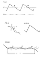
- the composite color signal is in a relation shown as (A) in Fig. 2
- the output of the adder 4 is as shown as (B) in Fig.
- the reference numerals 6, 7 and 8 denote a B-Y demodulator, a G-Y demodulator, and an R-Y demodulator, respectively.
- the reference numeral 9 denotes a voltage controlled oscillator for generating a color subcarrier wave of 4.433618 MHz and the output thereof is supplied through an amplifying circuit 10 and a phase shifter 11 to the B-Y demodulator 6 and the R-Y demodulator 8, with a predetermined phase difference (generally a difference of 90°) therebetween and is also applied to a phase comparator 13 of a phase locked loop type color synchronizing loop.
- the phase comparator 13 compares the phases a color burst of a predetermined phase extracted from the output (shown as ( B ) in Fig. 2) of the above described adder 4 by means of a color burst gate 12, and the above described color subcarrier wave and the output from the phase comparator 13 is applied through a low pass filter 14 to the voltage contorolled oscillator 9 as a control voltage.
- the reference numeral 15 denotes a sweeper circuit provided for assuring color synchronization by the output of the above described phase comparator 13 and is adapted to provide a stepwise sweep voltage waveform
- the reference numeral 16 denotes a means for providing a pulse voltage of a predetermined frequency (for example a repetition frequency of the color burst in the case where the horizontal frequency is f H ) for making stepwise the output of the above described sweeper circuit 15.
- the reference numeral 17 denotes a color killer circuit responsive to the G-Y demodulator 7 and the output of the R-Y demodulator 8 during the color burst period for disabling a function of the color amplifier 1 on the occasion of reception of monochrome broadcasting or on the occasion of abnormal reception of color broadcasting.
- the output of the color killer circuit 17 is simultaneously applied to the sweeper circuit 15 to disable the sweeper circuit 15 on the occasion of normal reception (such as in proper color synchronization) of the color broadcasting and otherwise to enable the same. Accordingly, as to be described subsequently the color killer circuit 17 serves to detect abnormalities of the outputs from the R-Y demodulator and the G-Y demodulator in the case where the switching operation of the PAL switch is not normal, and to control the operation of the phase locked loop type color synchronizing circuit upon detection of a normal output of the respective demodulators 7 and 8 in the case where the switching operation of the PAL switch is normal.
- the reference numeral 24 denotes a killer ineffective rendering means for preventing the color amplifier 1 from being stopped during at least the color burst period even when the color amplifier 1 is to be stopped by rendering ineffective the killer output being applied to the color amplifier 1 during the horizontal blanking period including the color burst period or the color burst as a function of the pulses P2.
- the reference numeral 20 denotes a PAL switch structured to alternately for each 1 H the output of the subtractor 5 through the phase shifter 18 or through the direct path 19 so that the same may be applied to the R-Y demodulator 8 and the PAL switch makes a switching operation responsive to the output of a flip-flop 21.
- the flip-flop 21 is driven responsive to the trigger pulses P3 of the horizontal frequency and the trigger pulses P3 are applied through the switch 22 to the flip-flop 21.
- the switch 22 is in an on state on the occasion of normal reception but is once turned off during a predetermined time period in the case where the above described phase locked loop type color synchronizing circuit is not locked, whereby the trigger pulses are rendered ineffective by one.
- Such driving of the switch 22 is performed by an extracting driving means 23 coupled to a sweeper circuit 15. In the case where the phase locked loop type color synchronizing circuit is locked, the extracting driving circuit 23 is disabled and accordingly the switch 22 remains closed.
- a vibrator 25 including LiT0 3 as a base material comes to show the zero impedance at the resonance frequency (4.433618 MHz) and therefore the base of one transistor T25 constituting a differential pair is supplied with the following voltage.
- the differential pair transistors T24 and T25 amplify the following difference voltage:
- the collector outputs of the differential pair transistors T24 and T25 are e24 and e25, respectively, the phases of the collector outputs e24 and e25 are different by 180°.
- the voltage e24 is applied through the emitter follower transistor T3 and through the point (e) to the phase shifting circuit 26 constituted by a resistor R A and a capacitor C A .
- the voltages eR and eC have a phase difference of 90° in the case where the impedances of the resistor R A and the capacitor C A are equal to each other.
- the voltages eR and eC are applied to the differential pair transistors T14 and T15; and T16 and T17.
- Fig. 5 shows a phase comparator 13 and a burst gate 12. These circuits are formed together as a double balance type differential circuit, in which the base of one transistor T131 of the lower stage differential pair transistors T130 and T131 is biased in a fixed manner by the voltage VOl, while the base of the other transistor T130 is supplied with the composite color signal from the color amplifier 1.
- the constant current source transistor T132 is supplied with the burst gate pulse Pl at the base thereof, whereby the same is rendered conductive only during the burst gate pulse period and only the color burst is extracted from the above described composite color signal to provide the same at the collectors of the lower stage differential pair transistors T130 and T131, which is supplied to the emitters of the upper stage differential pair transistors T126 and T127; and T128 and T 129.
- the bases of the transistors T127 and T128 out of the upper stage differential pair transistors T126 and T127; and T128 and T129 are supplied with a fixed bias V02, while the bases of the transistors T126 and T129 are supplied with the color subcarrier wave CW from the above described voltage controlled oscillator 9, whereby phase comparison of the color burst and the color subcarrier wave are made by way of multiplication.
- the first output appears at the point (g) where the collectors of the transistors T126 and T128 are commonly connected and the second output appears at the point (h) where the collectors of the transistors T 127 and T129 are commonly connected.
- the first and second outputs are of opposite phases to each other and the first output appears at the point (i) as the collector output of the transistor T135 from the current mirror circuit 28 implemented by the transistors T133, T134 and T135 and the resistors R153, R154 and R155 through the current mirror circuit 27 implemented by the transistors T120, T121 and T122 and the resistors R146, R147 and R148.
- the second output is obtained at the point (i) as the output of the transistor T124 through the current mirror circuit 29 implemented by the transistors T123, T124 and T125 and the resistors R149, R150 and R151.
- Fig. 6 shows the switching operation of the transistor responsive to the color burst and the color subcarrier wave CW and the output waveform based on the above described switching operation and in particular shows a signal of a beat frequency, i.e. a phase comparison output appearing as (C) in Fig. 6, by taking an example in the case where the color subcarrier wave CW shown as (B) in Fig. 6 as shifted by -if with respect to the color burst shown as (A) in F ig. 6.
- the output signal is supplied from the point (i) through a low pass filter 14 formed as a dual time constant circuit (a high frequency filter is formed with the resistor R152 and the capacitor C D and a low frequency filter is formed with the resistor R152 and the capacitor Cc in Fig. 5) to the above described voltage controlled oscillator 9 as a control voltage.
- a low pass filter 14 formed as a dual time constant circuit (a high frequency filter is formed with the resistor R152 and the capacitor C D and a low frequency filter is formed with the resistor R152 and the capacitor Cc in Fig. 5) to the above described voltage controlled oscillator 9 as a control voltage.
- the abscissa indicates the time and the ordinate indicates the above described control voltage and the curve A merely shows the output of the above described phase comparator 13 in the case where the phase locked loop is not rendered effective, i.e. in the case where the automatic color synchronization is not rendered effective.
- the oscillation frequency of the voltage controlled oscillator 9 becomes lower and the beat frequency also becomes lower, whereas since the control voltage is negative during a period of t6 - t12, the beat frequency becomes higher as shown by the curve B in Fig. 7.
- the curve B crosses the potential E for making stable oscillation of 4.433618 MHz at two points Zl and Z2; however, at the point Zl the operation is in a direction for decreasing the oscillation frequency and hence is in the direction away from the stable point and therefore a beat signal is further continually generated.
- the operation is in the direction for increasing the oscillation frequency to be close to the stable point of 4.433618 MHz and therefore the voltage controlled oscillator 9 becomes stabilized when the point Z2 is reached and thereafter no beat signal is generated.
- the embodiment employs an LiTa vibrator 25 as a vibrator of the voltage controlled oscillator 9. Employment of such LiTa vibrator brings about an advantage of extreme inexpensiveness of a vibrator as compared with the case where a quartz vibrator is employed and further brings about another merit set forth in the following.
- the frequency variable range as a function of the control voltage of the voltage controlled oscillator employing the LiTa vibrator is as broad as approximately +7 kHz due to the small quality factor of the LiTa vibrator 25 and is approximately ten times as compared with the frequency variable range of the conventional voltage controlled oscillator employing a quartz vibrator being approximtaly +700 Hz.
- the frequency distribution appears at 1 H interval with 4.433618 MHz as the center, as shown in Fig. 8.
- the frequency of 4.433618 MHz is necessary and, since there are intervals of +1 H from 4.433618 MHz to the adjacent frequency component, even in the case of the voltage controlled oscillator employing the LiTa vibrator the color synchronizing circuit will not make malfunction responsive to the adjacent frequency component.
- the frequency variable range of the voltage controlled oscillator employing the LiTa vibrator is approximately ten times, as_described previously, as compared with a case where the quartz vibrator is employed and therefore a pull-in range of the phase locked loop employing the voltage controlled oscillator employing the LiTa vibrator is also approximately ten times.
- a problem is involved that an anti-noise characteristic on the occasion of a weak electric field intensity is degraded (on the occasion of a weak electric field intensity generally a noise becomes conspicuous and this noise could make the apparatus operable).
- the embodiment is adapted such that the beat signal is applied to the low pass filter 14 formed as a dual time constant circuit shown in Fig. 5 to full attenuation (say ) whereby a frequency pull-in range is made narrow, thereby to improve an anti-noise characteristic on the occasion of a weak electric field intensity to be commensurate with that in case where a quartz vibrator is employed.
- the resistor R of the low pass filter 14 is 390 ⁇ the capacitor C C is 4.7 ⁇ F, the capacitor C D is 10000 pF, and the resistor R152 is 500 ⁇ .
- the embodiment shown employs a sweeper circuit 15 so that the above described beat signal is superimposed on the sweep voltage, whereby the beat signal is made to reach the stable potential of 4.433618 MHz, thereby to lock the phase locked loop.
- the sweep voltage waveform is selected to be not a mere sawtooth waveform but to be a stepwise waveform to be described subsequently.
- phase locked loop type color synchronization is not locked even when the sweep voltage waveform is superimposed.
- the above described stepwise waveform is aimed to eliminate such inconvenience. For example, considering a case of a phase locked loop in which an intermittent signal as shown as (B) in Fig. 11 is used as a reference signal, when a mere sawtooth waveform voltage is used as a sweep voltage being superimposed as shown in Fig.
- a locking operation is about to be made to the stable potential E at the point Xl shown as (A) in Fig. 11 but, since the information as a reference signal is intermittent, the phase compared output of the phase locked loop is not enough and a lock operation is not performed and thus even at the following point X2 of the fall of the sawtooth waveform likewise a lock operation is not performed. Meanwhile, a lock operation does not take place at the rise of the sawtooth waveform, not particularly shown, inasmuch as the same is steep, as is needless to say.
- the embodiment shown employs a sweep voltage waveform of a stepwise waveform as shown in Fig. 13 (since only the fall is used in the embodiment a stepwise waveform at the fall portion is sufficient), the sweep voltage does not decrease at every T period as shown in Fig. 14 and therefore at the T period close to the stable potential E the comparison output (the beat signal between the color burst and the color subcarrier wave) from the phase comparator 13 crosses the stable potential E several times as shown in Fig. 14, whereby chances of being locked are met at the points Z4, Z5 and Z6.
- the color burst of the intermittent signal is utilized for a plurality of lines (16 H) in the T period and a control signal of an ample one is obtained irrespective of the time constant of the low pass filter 14, with the result that a lock operation to the stable potential E is assured.
- the sweeper circuit 15 will be described with reference to the embodiment shown in Fig. 15.
- the capacitor C C of the low pass filter 14 (the filter is also shown in Fig. 5) has not been charged, assuming that the potential at the point (k) is El, the potential at the point (1) becomes El - Vf, where Vf is the base/emitter voltage on the occasion of conduction of the transistor. Since the capacitor C c has not been charged, the potential at the point (m) is 0 and the transistors T27 and T29 are placed in a cutoff state.
- the transistor T30 Since the transistor T30 has been placed in a cutoff state as described previously, the above described current does not flow through the transistor T30. As the capacitor C c is charged, the potential at the point (m) increases, whereby the potential at the point (n) accordingly increases. Since the transistor T32 as well as the above described transistors T31 and T40 are in an on state, a potential difference occurring across the resistor R46 increases and the potential at the point (1) also increases; however, the voltage El is exceeded, the transistor T37 in turned off and instead the transistor T39 is turned on and accordingly the potential at the point (1) is clamped to the value of El + Vf.
- the differential pair transistors T34 and T35 are operated such that the transistor T34 is turned on and the transistor T35 is turned off.
- the transistor T34 is turned on, the transistors T31, T32 and T40 are turned off.
- the transistor T31 is turned off, a charging current comes not to flow to the capacitor C C and the capacitor C c is not charged, with the result that the capacitor C c starts discharging.
- the transistor T40 is turned off, the transistor T47 comes not to be supplied with a base current, whereby the transistor T47 is turned off.
- the sweep voltage is a mere sawtooth waveform as shown in Fig. 10; however, the base of the transistor Q36 is supplied with a pulse of the frequency of from the pulse supply means 16 (Fig. 1) during the fall of the above described sweep waveform and therefore the transistor Q36 is turned on/off, whereby the transistor T30 is turned off/on and the potential at the point (m) and the potential at the point (q) become a stepwise waveform during the fall period, as shown Fig. 13.
- the transistor Q36 is turned off and therefore the transistor T30 is placed in an on state (because the base bias being applied through the path of the voltage source +Vcc 3 the resistor R49 + the resistor R39 ⁇ the transistor T30 is not rendered ineffective) and the electric charge in the capacitor C C is discharged through the collector and emitter of the transistor T30 and the resistor R36, whereby the potentials at the points (m) and (q) decrease.
- the period of the sweep voltage waveform is selected such that the period is 500 - 600 times of the horizontal period, as an example.
- the color killer circuit 17 produces a color killer signal responsive to the output during the color burst period of the R-Y demodulator 8 and the B-Y demodulator 7 as shown in Fig. 1.
- the output of the R-Y demodulator is applied from the line 31 to the base of the emitter follower transistor T76 through the low pass filter 32 including the resistor R101 and the capacitor C2 and is applied to the base of the transistor T77 forming the differential pair for the comparator 33 through the resistor R95 at the emitter side of the transistor T76.
- the output of the G-Y demodulator is applied from the line 34 to the base of the emitter follower transistor T79 through the low pass filter 35 including the resistor R108 and the capacitor C10 and is directly applied to the base of the other transistor T78 constituting the above described comparator 33 from the emitter of the transistor T79.
- the R-Y channel and the G-Y channel have been set in the same conditions, for example, the direct current biases from the demodulator applied to the lines 31 and 34 are the same and the resistors R101 and R108 and the capacitors C2 and C10 have been selected to be the same values, respectively, and so on; however the output of the R-Y demodulator is applied through the resistor R95 to the comparator 33 so that the output being applied is made small by a voltage drop across the resistor R95 as compared with the output of the G-Y demodulator.
- the said voltage drop is approximately 0.3 V.
- the output of the above described comparator 33 is applied to the integrating circuit 37 through the current mirror circuit 36 formed with the transitors T73, T74 and T75 and the resistors R92, R93 and R94 and is smoothed by the integrating circuit 37.
- the thus smoothed output is applied to the differential pair transistors T70 and T71 through the emitter follower transistor T72 (as regards the supplied bias thereto, the fixed potential Vl is directly applied to the base of the transistor T70 and is applied through the diode D10, the resistor R87, the base/emitter of the transistor T72 to the base of the transistor T71) and is further applied from the collector of the emitter grounded transistor T69 to the color amplifier 1 shown in Fig.
- the above described comparator 33 is operable only during the period of the burst gate pulse Pl applied to the base of the constant current source transistor T83 and is otherwise inoperable. Therefore, the output portion other than the color burst period out of the output from the R -Y demodulator and the output from the G-Y demodulator obtained from the lines 31 and 34 does not affect at all the color killer operation.
- the base potentials of the differential pair transistors T77 and T78 of the comparator 33 have been selected in advance such that the base potential of the transistor T78 is higher and therefore the transistor T77 has been uurned off and the transistor T78 has been turned on. Therefore, no current flows through the current mirror circuit 36 and the capacitor C E of the integrating circuit 37 has not been charged and the potential at the point (u) does not increase. Therefore, the differential pair transistors T70 and T71 at the output side are operated such that the transistor T70 is turned on and the transistor T71 is turned off.
- the transistor T69 is turned on responsive to the on state of the above described transistor T70 and the high level voltage is developed at the first output point O1 for stopping the color amplifier 1.
- the signal at the first output point 01 is applied through the color ineffective rendering means 24 and therefore does not stop the color amplifier 1 at least during the color burst period.
- the transistor T68 is turned off resposive to the off state of the transistor T71 and no voltage is generated at the second output point 02 for stopping the sweeper circuit 15 and accordingly the sweeper circuit 15 is placed in an enabled state.
- the color burst supplied from the subtractor 5 to the R-Y demodulator 8 is of the same phase as that of the demodulation axis of the R-Y demodulator, as shown as (D) in Fig. 2 and therefore the color burst demodulated output of the R-Y demodulator 8 is a positive voltage, whereby a potential at the line 31 increases and accordingly the base current of the transistor T77 also increases more than a predetermined value.
- the G-Y demodulator 7 receives the demodulated outputs from the R-Y demodulator and the B-Y demodulator to matrix the same, so that the same provides the demodulated outputs which are decreased to as small as approximately as compared with the outputs of the R-Y demodulator and the B-Y demodulator; however, the color burst demodulated output of the R-Y demodulator is plus and.the color burst demodulated output of the B-Y demodulator is minus on the occasion of the above described normal reception, so that the matrix output of the demodulated outputs of these demodulators 8 and 6 is approximtaly 0 V and only a direct current bias is provided from the beginning from the output line of the G-Y demodulator through the line 34.
- the states of the transistors T77 and T78 are reversed such that the transistor T77 is turned on and the transistor T78 is turned off.
- the transistor T77 is turned on, a current flows through the current mirror circuit 36 and a current for charging the capacitor C E flows through the point (u) and therefore the potential at the point (u) increases.
- the base potential of the transistor T72 also increases as the potential at the point (u) increases and the differential pair transistor T70 is turned off while the transistor T71 is turned on.
- the transistor T70 is turned off, no base current is supplied to the transistor T69 and the transistor T69 is turned off responsive to turning off of the transistor T70 and no voltage for stopping the operation of the color amplifier 1 is generated at the first output point 01. Therefore, the color amplifier 1 normally operates.
- the transistor T68 is turned on responsive to turning on of the transistor T71 and the high level is generated at the second output point 02. Since the high level voltage is applied to the base of the transistors T42 and T43 of the sweeper circuit 15, the transistors T42 and T43 are turned on and the base potentials of the transistors T30 and T36 are clamped to the ground potential, whereby the transistor T30 is fixed to off and the differential pair T34 and T35 are disabled while the sweep operation of the sweeper circuit 15 is stopped.
- the color burst being applied to the R-Y demodulator 8 is of the polarity opposite to the demodulating axis of the R-Y demodulator 8, as shown as (E) in Fig. 2 and the color burst demodulated output of the R-Y demodulator 8 becomes minus and the output from the supply line 31 becomes small. Since the phase of the color burst supplied from the adder 4 to the B-Y demodulator 6 at that time remains unchanged, the color burst demodulated output of the B-Y demodulator 6 remains minus.
- the color burst demodulated output of the G-Y demodulator 7 is also provided in the plus direction, although a little.
- the transistors T77 and T78 are operated such that the transistor T78 is turned on and the transistor T 77 is turned off, whereby no current flows in the current mirror circuit 36 and the potential at the point (u) does not increase, whereby the color amplifier 1 is stopped (although the same is not stopped by means of the color ineffective rendering means 24 during the color burst period), while the sweep circuit 15 starts a sweep operation, whereby the phase locked loop type color synchronizing circuit is not locked.
- the Fig. 16 color killer circuit comprises an auxiliary circuit 38 for promptly discharging the electric charge in the capacitor C E in the case where color synchronization is disturbed and the like for preventing a color noise from appearing on the screen and the auxiliary circuit 38 comprises differential pair transistors T81 and T82, a constant current source transistor T84 therefor and a resistor R102 and a reverse current preventing diode Dll.
- the R-Y demodulated output and the G-Y demodulated output being applied to the auxiliary circuit 38 are applied in a relation of the level opposite to those applied to the above described comparator 33.
- the output from the R-Y demodulator is supplied from the emitter of the emitter follower transistor T76 directly to the base of the transistor T82, while the output from the G-Y demodulator is supplied from the emitter of the emitter follower transistor T79 through the resistor R100 of the voltage drop of 0.3 V to the base of the transistor T 81 and therefore are in the relation opposite to the output of the demodulator being applied to the comparator 33.
- the base of the constant current source transistor T84 is supplied with a burst gate pulse commonly to the constant current source transistor T83 for the comparator 33 and accordingly the auxiliary circuit 38 also operates only during the color burst period.
- the transistor T82 Since the base potential of the transistor T 82 has been selected to be higher than the base potential of the transistor T81, the transistor T82 is turned on and the transistor T81 is turned off in the absence of the color burst and in the case where the reception state is normal even in the presence of the color burst, no influence is exerted upon the potential at the point (u). However, on the occasion of reception of the color broadcasting of a weak electric field intensity, for example, the phase of the color burst is liable to change at random. In the case of such disturbed color burst or the case where the switching mode of the PAL switch 20 is not normal, it could happen that the negative color burst demodulated output is obtained from th R-Y demodulator 8.
- the transistor T81 of the auxiliary circuit 38 is turned on and the electric charge in the capacitor C E is instantaneously discharged through the path of the capacitor C E 7 the diode D11 ⁇ the transistor T81 4 the constant current source transistor T84 and the resistor R102 ⁇ the ground.
- Fig. 17 shows a color killer circuit of another embodiment.
- the Fig. 17 embodiment is different from the Fig. 16 embodiment in that the line 34 is connected to the B-Y demodulator 6 and another transistor T80 is added in parallel with the transistor T79 and the G-Y demodulator 7 is connected through the line 39 to the base of the transistor T80.
- the Fig. 17 circuit is suited for a television receiver adapted to be receivable of NTSC broadcasting and PAL broadcasting.
- the transistor T158 connected to the point (w) is turned on so that the base of the transistor T80 is brought to the potential of the ground, whereby the output of the G-Y demodulator is interrupted and the comparator 33 and the auxiliary circuit 38 are operable only responsive to the output of the R-Y demodulator and the output of the B-Y demodulator.
- the transistor T158 is turned off so that the output of the G-Y demodulator is utilized.
- the transistors T42 and T43 are maintained in an off state by means of the color killer circuit 17 and therefore the sweeper circuit 15 performs an sweep operation described previously.
- the transistors T42 and T43 are turned on and the sweeper circuit 15 is fixed to a stopped state, whereby the color synchronizing phase locked loop is locked.
- the output of the phase comparator 13 becomes zero in terms of the direct current. This is shown in a current waveform as (A) in Fig. 18.
- the frequency of a beat signal (a beat of the color subcarrier wave and the color burst) of the output from the phase comparator 13 is as low as being deemed as substantially a direct current and therefore the time constant of the low pass filter 30 becomes large and the input impedances of the emitter follower transistors T27 and T29 (Fig. 15) are also large and the gain of the phase comparator 13 becomes large.
- a current flows by an amount (a hatched portion) associated with deviation of the phase and the frequency as shown as (B) in Fig.
- the abscissa indicates the deviation amount of the color subcarrier wave and the ordinate indicates the output of the phase detector.
- the sweeper circuit 15 continues a sweep operation by virtue of the color killer circuit 17 so that the phase locked loop type color synchronizing circuit is not locked, as described previously; however, without any means for returning the switching operation to a normal state, the PAL switch 20 will not turn to a normal switch operation.
- Such means is implemented by a switch 22 provided in a supply path of the trigger pulses P3 to the flip-flop 21 and an extracting driving means 23 for controlling the switch 22.
- the color burst of each line is directed upward as shown as (D) in Fig.
- the color burst demodulated output of the R-Y demodulator 8 becomes as shown as (D) in Fig. 19.
- the phase locked loop type color synchronizing circuit is locked at a portion directed upward.
- the portion F is a case where color synchronization is disturbed and therefore the color burst demodulated output of the R-Y demodulator 8 occurs both in the plus direction and the minus direction and in such a case the capacitor C E is not charged by the auxiliary circuit 38 in the color killer circuit 17 and therefore the sweep operation of the sweeper circuit 15 is not stopped, so that phase locked loop type color synchronizing circuit is not locked; however, the same is locked at the portion J of .
- the curve (D) in Fig. 19 the portion F is a case where color synchronization is disturbed and therefore the color burst demodulated output of the R-Y demodulator 8 occurs both in the plus direction and the minus direction and in such a case the capacitor C E is not charged by the auxiliary circuit 38 in the color killer circuit 17 and therefore the sweep operation of
- the sweeper circuit 15 is stopped and the extracting driving means 23 is also stopped so that the switch 22 remains closed and the trigger pulses P3 are not extracted any more and accordingly the PAL switch 20 operates in a normal switching mode.
- the switching mode of the PAL switch 20 is set in a normal state.
- extraction of the trigger pulses P3 may be executed not during a predetermined potential period T of the stepwise sweep voltage but instead in a fall period t of the sweep voltage as a matter of course and even in such a case color synchronizing circuit is locked during the predetermined potential period T.
- the Fig. 15 embodiment is adapted such that extraction of the trigger pulses.P3 and hence forced reversion of the switching mode of the PAL switch 20 is executed during the fall period.t.
- the pulses of are supplied from the pulse supply means 16 to the base of the transistor Q36 whereby the sweep voltage waveform becomes stepwise.
- the transistor T44 having the base connected through the resistor R80 to the emitter of the discharging transistor T30 is rendered conductive upon application of a base bias when the transistor T30 is turned on and accordingly during the fall period t of the sweep voltage. Accordingly, the emitter of the transistor T45 is connected to the ground and the transistor T45 is turned on or off depending on the state of the base thereof.
- the base thereof is supplied with one pulse from the second pulse supply means 40 during the above described period t so that the transistor T45 is turned on only during the pulse period.
- the transistor T67 is also turned on and the potential at the point (x) increases up to +Vcc and the switch 22 is turned off, whereby the trigger pulses P3 are rendered ineffective by one.
- the pulse of the second pulse supply means 40 is of a pulse width enough to cover the above described one trigger pulse.
- the transistor T45 is turned off and accordingly the transistor T67 is turned off, so that the potential at the point (x) does not increase and the switch 22 is turned on.
- the phase locked loop type color synchronizing circuit When the phase locked loop type color synchronizing circuit is locked, the high level is applied from the color killer circuit 17 to the bases of the transistors T42 and T43 and the transistors T30 and T36 are fixed to be off, whereby the base potential of the transistor T44 becomes 0 and the transistor T44 is fixed to be off. Therefore, irrespective of whether the pulse is supplied from the second pulse supply means 40 or not, the transistor T45 is brought to an off state and accordingly the switch 22 remains in an on state. Referring to Fig. 15, the transistor T67 and the switch 22 are connected to the line 41 of the variable resistor VR for manually adjusting the gain of the color amplifier 1.
- the color amplifier 1 is cut off during the scanning period responsive to the output of the color killer circuit when the phase locked loop type color synchronizing circuit is not locked so that a carried color signal is stopped. Therefore, it does not matter even if a voltage set by the gain adjusting variable resistor VR is changed as described above when the phase locked loop type color synchronizing circuit is not locked. In the case where the phase locked loop type color synchronizing circuit is locked, the transistor T67 is cut off, as is clear from the foregoing description and therefore the voltage set by the gain adjusting variable resistor VR is applied to the color amplifier 1 without being disturbed.
- an advantage of utilizing the color gain adjusting variable resistor VR for the purpose of controlling the switch 22 is that the terminal pin for withdrawing a control voltage from inside an integrated circuit for controlling the switch in the case where the circuit is implemented in an integrated circuit can be shared with an external connection pin for a color gain adjusting variable resistor, resulting in a decrease of the number of terminal pins by one.
- the transistors T44, T45, and T67 and the resistor R52 and the pulse supply 40 form the extracting driving means 23 shown in Fig. 1.
- the present invention achieves assured control of switching mode of a PAL switch - with a novel structure and is of much utility.
Landscapes
- Engineering & Computer Science (AREA)
- Multimedia (AREA)
- Signal Processing (AREA)
- Processing Of Color Television Signals (AREA)
Applications Claiming Priority (2)
| Application Number | Priority Date | Filing Date | Title |
|---|---|---|---|
| JP12758480A JPS5752287A (en) | 1980-09-11 | 1980-09-11 | Color signal circuit of pal color television set |
| JP127584/80 | 1980-09-11 |
Publications (4)
| Publication Number | Publication Date |
|---|---|
| EP0047995A2 true EP0047995A2 (de) | 1982-03-24 |
| EP0047995A3 EP0047995A3 (en) | 1984-11-28 |
| EP0047995B1 EP0047995B1 (de) | 1987-07-29 |
| EP0047995B2 EP0047995B2 (de) | 1990-08-08 |
Family
ID=14963676
Family Applications (1)
| Application Number | Title | Priority Date | Filing Date |
|---|---|---|---|
| EP19810107183 Expired EP0047995B2 (de) | 1980-09-11 | 1981-09-11 | Farbfernsehsignal-Verarbeitungsschaltung für ein PAL-System |
Country Status (4)
| Country | Link |
|---|---|
| EP (1) | EP0047995B2 (de) |
| JP (1) | JPS5752287A (de) |
| AU (1) | AU548798B2 (de) |
| DE (1) | DE3176338D1 (de) |
Families Citing this family (1)
| Publication number | Priority date | Publication date | Assignee | Title |
|---|---|---|---|---|
| JPS6130892A (ja) * | 1984-07-23 | 1986-02-13 | Pioneer Electronic Corp | Pal方式カラ−ビデオ信号再生装置における色同期回路 |
Family Cites Families (3)
| Publication number | Priority date | Publication date | Assignee | Title |
|---|---|---|---|---|
| GB1212710A (en) * | 1967-12-12 | 1970-11-18 | Philips Nv | Circuit arrangement for synchronizing a pal line switch |
| US4133002A (en) * | 1977-09-26 | 1979-01-02 | Rca Corporation | Pal identification circuit |
| JPS5469018A (en) * | 1977-11-11 | 1979-06-02 | Sony Corp | Color demodulator circuit |
-
1980
- 1980-09-11 JP JP12758480A patent/JPS5752287A/ja active Granted
-
1981
- 1981-09-02 AU AU74894/81A patent/AU548798B2/en not_active Expired
- 1981-09-11 DE DE8181107183T patent/DE3176338D1/de not_active Expired
- 1981-09-11 EP EP19810107183 patent/EP0047995B2/de not_active Expired
Also Published As
| Publication number | Publication date |
|---|---|
| DE3176338D1 (en) | 1987-09-03 |
| EP0047995B2 (de) | 1990-08-08 |
| JPS637508B2 (de) | 1988-02-17 |
| AU548798B2 (en) | 1986-01-02 |
| EP0047995B1 (de) | 1987-07-29 |
| JPS5752287A (en) | 1982-03-27 |
| EP0047995A3 (en) | 1984-11-28 |
| AU7489481A (en) | 1982-03-18 |
Similar Documents
| Publication | Publication Date | Title |
|---|---|---|
| US3740456A (en) | Electronic signal processing circuit | |
| US4241363A (en) | Comb filter circuit | |
| US4470066A (en) | Circuit arrangement for adjusting the direct current level of a video signal | |
| CA1075356A (en) | Vir control apparatus for color television receiver | |
| US5457500A (en) | Color TV receiver using quadrature-phase synchronous detector for supplying signal to chrominance circuitry | |
| US3806634A (en) | Multiplex color television demodulator | |
| US3740461A (en) | Detector circuits with self-referenced bias | |
| FI75707C (fi) | Kretsarrangemang foer foerbaettrande av kantskaerpa vid videosignaler. | |
| SE438937B (sv) | Stromkrets for att undertrycka storningar i luminanssignaler hos en fergtelevisionsanordning | |
| US4425576A (en) | Picture stabilizing circuit in color television receiver | |
| US4263675A (en) | AFT circuit | |
| US4413274A (en) | Color synchronizing circuit | |
| EP0047995B1 (de) | Farbfernsehsignal-Verarbeitungsschaltung für ein PAL-System | |
| US4573069A (en) | Chrominance fine gain control in a digital television receiver | |
| US2908748A (en) | Color television chroma control system | |
| US4295161A (en) | Keyed noise filter in a television receiver | |
| US4229759A (en) | Signal detector including sample and hold circuit with reduced offset error | |
| US3806635A (en) | Multiplex color television demodulator | |
| CA1067615A (en) | Sync separator | |
| US4216493A (en) | Chrominance signal processing circuit in color television receiver | |
| US2502195A (en) | Synchronizing system | |
| EP0616474A2 (de) | Fernsehsschaltung die ein Farbsynchronsignal verwendet | |
| US4577217A (en) | Encoding circuit for a SECAM color television transmission | |
| US4337478A (en) | Composite timing signal generator with predictable output level | |
| AU596768B2 (en) | Afc apparatus |
Legal Events
| Date | Code | Title | Description |
|---|---|---|---|
| PUAI | Public reference made under article 153(3) epc to a published international application that has entered the european phase |
Free format text: ORIGINAL CODE: 0009012 |
|
| AK | Designated contracting states |
Designated state(s): CH DE GB NL |
|
| PUAL | Search report despatched |
Free format text: ORIGINAL CODE: 0009013 |
|
| AK | Designated contracting states |
Designated state(s): CH DE GB LI NL |
|
| 17P | Request for examination filed |
Effective date: 19841214 |
|
| GRAA | (expected) grant |
Free format text: ORIGINAL CODE: 0009210 |
|
| AK | Designated contracting states |
Kind code of ref document: B1 Designated state(s): CH DE GB LI NL |
|
| REF | Corresponds to: |
Ref document number: 3176338 Country of ref document: DE Date of ref document: 19870903 |
|
| PLBI | Opposition filed |
Free format text: ORIGINAL CODE: 0009260 |
|
| 26 | Opposition filed |
Opponent name: N.V. PHILIPS' GLOEILAMPENFABRIEKEN Effective date: 19880107 |
|
| NLR1 | Nl: opposition has been filed with the epo |
Opponent name: N.V. PHILIPS' GLOEILAMPENFABRIEKEN |
|
| PUAH | Patent maintained in amended form |
Free format text: ORIGINAL CODE: 0009272 |
|
| STAA | Information on the status of an ep patent application or granted ep patent |
Free format text: STATUS: PATENT MAINTAINED AS AMENDED |
|
| 27A | Patent maintained in amended form |
Effective date: 19900808 |
|
| AK | Designated contracting states |
Kind code of ref document: B2 Designated state(s): CH DE GB NL |
|
| NLR2 | Nl: decision of opposition | ||
| NLR3 | Nl: receipt of modified translations in the netherlands language after an opposition procedure | ||
| PGFP | Annual fee paid to national office [announced via postgrant information from national office to epo] |
Ref country code: DE Payment date: 20000904 Year of fee payment: 20 |
|
| PGFP | Annual fee paid to national office [announced via postgrant information from national office to epo] |
Ref country code: GB Payment date: 20000906 Year of fee payment: 20 |
|
| PGFP | Annual fee paid to national office [announced via postgrant information from national office to epo] |
Ref country code: CH Payment date: 20000922 Year of fee payment: 20 |
|
| PGFP | Annual fee paid to national office [announced via postgrant information from national office to epo] |
Ref country code: NL Payment date: 20000928 Year of fee payment: 20 |
|
| PG25 | Lapsed in a contracting state [announced via postgrant information from national office to epo] |
Ref country code: LI Free format text: LAPSE BECAUSE OF EXPIRATION OF PROTECTION Effective date: 20010910 Ref country code: GB Free format text: LAPSE BECAUSE OF EXPIRATION OF PROTECTION Effective date: 20010910 Ref country code: CH Free format text: LAPSE BECAUSE OF EXPIRATION OF PROTECTION Effective date: 20010910 |
|
| PG25 | Lapsed in a contracting state [announced via postgrant information from national office to epo] |
Ref country code: NL Free format text: LAPSE BECAUSE OF EXPIRATION OF PROTECTION Effective date: 20010911 |
|
| REG | Reference to a national code |
Ref country code: GB Ref legal event code: PE20 Effective date: 20010910 |
|
| REG | Reference to a national code |
Ref country code: CH Ref legal event code: PL |
|
| NLV7 | Nl: ceased due to reaching the maximum lifetime of a patent |
Effective date: 20010911 |