EP0048255B1 - Halbleitervorrichtung und deren herstellung - Google Patents
Halbleitervorrichtung und deren herstellung Download PDFInfo
- Publication number
- EP0048255B1 EP0048255B1 EP81900812A EP81900812A EP0048255B1 EP 0048255 B1 EP0048255 B1 EP 0048255B1 EP 81900812 A EP81900812 A EP 81900812A EP 81900812 A EP81900812 A EP 81900812A EP 0048255 B1 EP0048255 B1 EP 0048255B1
- Authority
- EP
- European Patent Office
- Prior art keywords
- tin
- substrate
- semiconductor
- region
- monocrystalline
- Prior art date
- Legal status (The legal status is an assumption and is not a legal conclusion. Google has not performed a legal analysis and makes no representation as to the accuracy of the status listed.)
- Expired
Links
- 239000004065 semiconductor Substances 0.000 title claims abstract description 70
- 238000004519 manufacturing process Methods 0.000 title claims description 5
- ATJFFYVFTNAWJD-UHFFFAOYSA-N Tin Chemical compound [Sn] ATJFFYVFTNAWJD-UHFFFAOYSA-N 0.000 claims abstract description 90
- 239000000758 substrate Substances 0.000 claims abstract description 53
- 239000000463 material Substances 0.000 claims abstract description 34
- WPYVAWXEWQSOGY-UHFFFAOYSA-N indium antimonide Chemical compound [Sb]#[In] WPYVAWXEWQSOGY-UHFFFAOYSA-N 0.000 claims abstract description 16
- MARUHZGHZWCEQU-UHFFFAOYSA-N 5-phenyl-2h-tetrazole Chemical compound C1=CC=CC=C1C1=NNN=N1 MARUHZGHZWCEQU-UHFFFAOYSA-N 0.000 claims abstract description 12
- 239000002019 doping agent Substances 0.000 claims abstract description 12
- 229910052732 germanium Inorganic materials 0.000 claims abstract description 12
- GNPVGFCGXDBREM-UHFFFAOYSA-N germanium atom Chemical compound [Ge] GNPVGFCGXDBREM-UHFFFAOYSA-N 0.000 claims abstract description 12
- 238000000034 method Methods 0.000 claims description 20
- 230000008569 process Effects 0.000 claims description 12
- 239000012535 impurity Substances 0.000 claims description 10
- XUIMIQQOPSSXEZ-UHFFFAOYSA-N Silicon Chemical compound [Si] XUIMIQQOPSSXEZ-UHFFFAOYSA-N 0.000 claims description 8
- 229910052710 silicon Inorganic materials 0.000 claims description 8
- 239000010703 silicon Substances 0.000 claims description 8
- 230000007704 transition Effects 0.000 claims description 5
- 238000000137 annealing Methods 0.000 claims description 2
- 230000006911 nucleation Effects 0.000 claims description 2
- 238000010899 nucleation Methods 0.000 claims description 2
- 238000002161 passivation Methods 0.000 claims 1
- 229910052751 metal Inorganic materials 0.000 abstract description 9
- 239000002184 metal Substances 0.000 abstract description 9
- 230000003993 interaction Effects 0.000 abstract description 3
- 238000001451 molecular beam epitaxy Methods 0.000 abstract 1
- 239000002210 silicon-based material Substances 0.000 abstract 1
- 230000005855 radiation Effects 0.000 description 8
- 230000008020 evaporation Effects 0.000 description 7
- 238000001704 evaporation Methods 0.000 description 7
- 229910052738 indium Inorganic materials 0.000 description 7
- APFVFJFRJDLVQX-UHFFFAOYSA-N indium atom Chemical compound [In] APFVFJFRJDLVQX-UHFFFAOYSA-N 0.000 description 7
- 229910000661 Mercury cadmium telluride Inorganic materials 0.000 description 5
- BASFCYQUMIYNBI-UHFFFAOYSA-N platinum Chemical compound [Pt] BASFCYQUMIYNBI-UHFFFAOYSA-N 0.000 description 5
- 230000008901 benefit Effects 0.000 description 4
- 230000004044 response Effects 0.000 description 4
- XKRFYHLGVUSROY-UHFFFAOYSA-N Argon Chemical compound [Ar] XKRFYHLGVUSROY-UHFFFAOYSA-N 0.000 description 3
- PZNSFCLAULLKQX-UHFFFAOYSA-N Boron nitride Chemical compound N#B PZNSFCLAULLKQX-UHFFFAOYSA-N 0.000 description 3
- GYHNNYVSQQEPJS-UHFFFAOYSA-N Gallium Chemical compound [Ga] GYHNNYVSQQEPJS-UHFFFAOYSA-N 0.000 description 3
- OKKJLVBELUTLKV-UHFFFAOYSA-N Methanol Chemical compound OC OKKJLVBELUTLKV-UHFFFAOYSA-N 0.000 description 3
- 229910052785 arsenic Inorganic materials 0.000 description 3
- RQNWIZPPADIBDY-UHFFFAOYSA-N arsenic atom Chemical compound [As] RQNWIZPPADIBDY-UHFFFAOYSA-N 0.000 description 3
- MCMSPRNYOJJPIZ-UHFFFAOYSA-N cadmium;mercury;tellurium Chemical compound [Cd]=[Te]=[Hg] MCMSPRNYOJJPIZ-UHFFFAOYSA-N 0.000 description 3
- 238000010276 construction Methods 0.000 description 3
- 229910052733 gallium Inorganic materials 0.000 description 3
- 230000035945 sensitivity Effects 0.000 description 3
- 230000003595 spectral effect Effects 0.000 description 3
- 229910006592 α-Sn Inorganic materials 0.000 description 3
- JBRZTFJDHDCESZ-UHFFFAOYSA-N AsGa Chemical compound [As]#[Ga] JBRZTFJDHDCESZ-UHFFFAOYSA-N 0.000 description 2
- ZOXJGFHDIHLPTG-UHFFFAOYSA-N Boron Chemical compound [B] ZOXJGFHDIHLPTG-UHFFFAOYSA-N 0.000 description 2
- 229910001218 Gallium arsenide Inorganic materials 0.000 description 2
- ZOKXTWBITQBERF-UHFFFAOYSA-N Molybdenum Chemical compound [Mo] ZOKXTWBITQBERF-UHFFFAOYSA-N 0.000 description 2
- VYPSYNLAJGMNEJ-UHFFFAOYSA-N Silicium dioxide Chemical compound O=[Si]=O VYPSYNLAJGMNEJ-UHFFFAOYSA-N 0.000 description 2
- 229910052786 argon Inorganic materials 0.000 description 2
- QVGXLLKOCUKJST-UHFFFAOYSA-N atomic oxygen Chemical compound [O] QVGXLLKOCUKJST-UHFFFAOYSA-N 0.000 description 2
- 230000015572 biosynthetic process Effects 0.000 description 2
- 229910052796 boron Inorganic materials 0.000 description 2
- 238000001816 cooling Methods 0.000 description 2
- 229910003460 diamond Inorganic materials 0.000 description 2
- 239000010432 diamond Substances 0.000 description 2
- 238000000407 epitaxy Methods 0.000 description 2
- PCHJSUWPFVWCPO-UHFFFAOYSA-N gold Chemical compound [Au] PCHJSUWPFVWCPO-UHFFFAOYSA-N 0.000 description 2
- 229910052737 gold Inorganic materials 0.000 description 2
- 239000010931 gold Substances 0.000 description 2
- 238000010438 heat treatment Methods 0.000 description 2
- 238000011065 in-situ storage Methods 0.000 description 2
- 239000010410 layer Substances 0.000 description 2
- 239000007769 metal material Substances 0.000 description 2
- 229910052750 molybdenum Inorganic materials 0.000 description 2
- 239000011733 molybdenum Substances 0.000 description 2
- 229910052760 oxygen Inorganic materials 0.000 description 2
- 239000001301 oxygen Substances 0.000 description 2
- 229910052697 platinum Inorganic materials 0.000 description 2
- 230000006641 stabilisation Effects 0.000 description 2
- WGPCGCOKHWGKJJ-UHFFFAOYSA-N sulfanylidenezinc Chemical compound [Zn]=S WGPCGCOKHWGKJJ-UHFFFAOYSA-N 0.000 description 2
- 229910002058 ternary alloy Inorganic materials 0.000 description 2
- 229910052984 zinc sulfide Inorganic materials 0.000 description 2
- 229910052582 BN Inorganic materials 0.000 description 1
- WKBOTKDWSSQWDR-UHFFFAOYSA-N Bromine atom Chemical compound [Br] WKBOTKDWSSQWDR-UHFFFAOYSA-N 0.000 description 1
- OKTJSMMVPCPJKN-UHFFFAOYSA-N Carbon Chemical compound [C] OKTJSMMVPCPJKN-UHFFFAOYSA-N 0.000 description 1
- GPXJNWSHGFTCBW-UHFFFAOYSA-N Indium phosphide Chemical compound [In]#P GPXJNWSHGFTCBW-UHFFFAOYSA-N 0.000 description 1
- BQCADISMDOOEFD-UHFFFAOYSA-N Silver Chemical compound [Ag] BQCADISMDOOEFD-UHFFFAOYSA-N 0.000 description 1
- 230000009471 action Effects 0.000 description 1
- 239000004411 aluminium Substances 0.000 description 1
- 229910052782 aluminium Inorganic materials 0.000 description 1
- XAGFODPZIPBFFR-UHFFFAOYSA-N aluminium Chemical compound [Al] XAGFODPZIPBFFR-UHFFFAOYSA-N 0.000 description 1
- -1 argon ions Chemical class 0.000 description 1
- 238000003491 array Methods 0.000 description 1
- 230000004888 barrier function Effects 0.000 description 1
- GDTBXPJZTBHREO-UHFFFAOYSA-N bromine Substances BrBr GDTBXPJZTBHREO-UHFFFAOYSA-N 0.000 description 1
- 229910052794 bromium Inorganic materials 0.000 description 1
- 229910052793 cadmium Inorganic materials 0.000 description 1
- BDOSMKKIYDKNTQ-UHFFFAOYSA-N cadmium atom Chemical compound [Cd] BDOSMKKIYDKNTQ-UHFFFAOYSA-N 0.000 description 1
- 229910052799 carbon Inorganic materials 0.000 description 1
- 238000003486 chemical etching Methods 0.000 description 1
- 230000000052 comparative effect Effects 0.000 description 1
- 150000001875 compounds Chemical class 0.000 description 1
- 238000009826 distribution Methods 0.000 description 1
- 238000002003 electron diffraction Methods 0.000 description 1
- 239000003822 epoxy resin Substances 0.000 description 1
- 239000011810 insulating material Substances 0.000 description 1
- 238000010849 ion bombardment Methods 0.000 description 1
- 238000010884 ion-beam technique Methods 0.000 description 1
- 230000000873 masking effect Effects 0.000 description 1
- QSHDDOUJBYECFT-UHFFFAOYSA-N mercury Chemical compound [Hg] QSHDDOUJBYECFT-UHFFFAOYSA-N 0.000 description 1
- 229910052753 mercury Inorganic materials 0.000 description 1
- 150000002739 metals Chemical class 0.000 description 1
- 238000003801 milling Methods 0.000 description 1
- 230000005501 phase interface Effects 0.000 description 1
- 238000000206 photolithography Methods 0.000 description 1
- 229920000647 polyepoxide Polymers 0.000 description 1
- 230000006335 response to radiation Effects 0.000 description 1
- 238000000682 scanning probe acoustic microscopy Methods 0.000 description 1
- 239000000377 silicon dioxide Substances 0.000 description 1
- 229910052709 silver Inorganic materials 0.000 description 1
- 239000004332 silver Substances 0.000 description 1
- 239000002356 single layer Substances 0.000 description 1
- 238000001228 spectrum Methods 0.000 description 1
- 239000010935 stainless steel Substances 0.000 description 1
- 229910001220 stainless steel Inorganic materials 0.000 description 1
- 239000000126 substance Substances 0.000 description 1
- 238000006467 substitution reaction Methods 0.000 description 1
- 229910052715 tantalum Inorganic materials 0.000 description 1
- GUVRBAGPIYLISA-UHFFFAOYSA-N tantalum atom Chemical compound [Ta] GUVRBAGPIYLISA-UHFFFAOYSA-N 0.000 description 1
- 229910052714 tellurium Inorganic materials 0.000 description 1
- PORWMNRCUJJQNO-UHFFFAOYSA-N tellurium atom Chemical compound [Te] PORWMNRCUJJQNO-UHFFFAOYSA-N 0.000 description 1
- 238000001931 thermography Methods 0.000 description 1
Images
Classifications
-
- H—ELECTRICITY
- H10—SEMICONDUCTOR DEVICES; ELECTRIC SOLID-STATE DEVICES NOT OTHERWISE PROVIDED FOR
- H10F—INORGANIC SEMICONDUCTOR DEVICES SENSITIVE TO INFRARED RADIATION, LIGHT, ELECTROMAGNETIC RADIATION OF SHORTER WAVELENGTH OR CORPUSCULAR RADIATION
- H10F10/00—Individual photovoltaic cells, e.g. solar cells
- H10F10/10—Individual photovoltaic cells, e.g. solar cells having potential barriers
- H10F10/16—Photovoltaic cells having only PN heterojunction potential barriers
- H10F10/164—Photovoltaic cells having only PN heterojunction potential barriers comprising heterojunctions with Group IV materials, e.g. ITO/Si or GaAs/SiGe photovoltaic cells
-
- H—ELECTRICITY
- H01—ELECTRIC ELEMENTS
- H01S—DEVICES USING THE PROCESS OF LIGHT AMPLIFICATION BY STIMULATED EMISSION OF RADIATION [LASER] TO AMPLIFY OR GENERATE LIGHT; DEVICES USING STIMULATED EMISSION OF ELECTROMAGNETIC RADIATION IN WAVE RANGES OTHER THAN OPTICAL
- H01S5/00—Semiconductor lasers
- H01S5/30—Structure or shape of the active region; Materials used for the active region
-
- H—ELECTRICITY
- H10—SEMICONDUCTOR DEVICES; ELECTRIC SOLID-STATE DEVICES NOT OTHERWISE PROVIDED FOR
- H10F—INORGANIC SEMICONDUCTOR DEVICES SENSITIVE TO INFRARED RADIATION, LIGHT, ELECTROMAGNETIC RADIATION OF SHORTER WAVELENGTH OR CORPUSCULAR RADIATION
- H10F77/00—Constructional details of devices covered by this subclass
- H10F77/10—Semiconductor bodies
- H10F77/12—Active materials
- H10F77/122—Active materials comprising only Group IV materials
-
- H—ELECTRICITY
- H01—ELECTRIC ELEMENTS
- H01S—DEVICES USING THE PROCESS OF LIGHT AMPLIFICATION BY STIMULATED EMISSION OF RADIATION [LASER] TO AMPLIFY OR GENERATE LIGHT; DEVICES USING STIMULATED EMISSION OF ELECTROMAGNETIC RADIATION IN WAVE RANGES OTHER THAN OPTICAL
- H01S5/00—Semiconductor lasers
- H01S5/30—Structure or shape of the active region; Materials used for the active region
- H01S5/3027—IV compounds
-
- H—ELECTRICITY
- H01—ELECTRIC ELEMENTS
- H01S—DEVICES USING THE PROCESS OF LIGHT AMPLIFICATION BY STIMULATED EMISSION OF RADIATION [LASER] TO AMPLIFY OR GENERATE LIGHT; DEVICES USING STIMULATED EMISSION OF ELECTROMAGNETIC RADIATION IN WAVE RANGES OTHER THAN OPTICAL
- H01S5/00—Semiconductor lasers
- H01S5/30—Structure or shape of the active region; Materials used for the active region
- H01S5/32—Structure or shape of the active region; Materials used for the active region comprising PN junctions, e.g. hetero- or double- heterostructures
- H01S5/3223—IV compounds
-
- Y—GENERAL TAGGING OF NEW TECHNOLOGICAL DEVELOPMENTS; GENERAL TAGGING OF CROSS-SECTIONAL TECHNOLOGIES SPANNING OVER SEVERAL SECTIONS OF THE IPC; TECHNICAL SUBJECTS COVERED BY FORMER USPC CROSS-REFERENCE ART COLLECTIONS [XRACs] AND DIGESTS
- Y02—TECHNOLOGIES OR APPLICATIONS FOR MITIGATION OR ADAPTATION AGAINST CLIMATE CHANGE
- Y02E—REDUCTION OF GREENHOUSE GAS [GHG] EMISSIONS, RELATED TO ENERGY GENERATION, TRANSMISSION OR DISTRIBUTION
- Y02E10/00—Energy generation through renewable energy sources
- Y02E10/50—Photovoltaic [PV] energy
- Y02E10/547—Monocrystalline silicon PV cells
Definitions
- the invention relates to a semiconductor device and the manufacture thereof; particularly a semiconductor device having a monocrystalline region of semiconductor material in intimate contact with a monocrystalline substrate.
- Such a device is one including, as semiconductor material, the material gallium arsenide. Regions of this material have been grown epitaxially, both gallium and arsenic, each a metallic material, being deposited in stoichiometric proportion by molecular beams produced in an ultra-high vacuum enclosure. This technique is described in the Journal of Applied Physics Vol 39 p 4032 (1968) in an article by J. R. Arthur.
- the semiconductor material silicon has also been grown epitaxially from a silicon beam in ultra high vacuum.
- contacts between metal leads and semi- conductor silicon regions are required, particular care being necessary to ensure that such contacts are ohmic. This is a factor having considerable bearing on the economics of mass production of large scale integrated silicon devices where many such contacts are requisite.
- Metal material has also been grown epitaxially on semiconductor substrates to provide either conductive contacts or metal Schottky barrier regions.
- growth of high purity silver, aluminium or gold on indium phosphide has been achieved at growth temperatures of about 30°C, this being the lowest reported temperature for epitaxy of these metals on a III-V compound semi-conductor surface.
- CF RFC Farrow et al Proc 4th Int Conf on Vapour Growth and Epitaxy (ICVGE-4) Nagoya, Japan, (July 9-13, 1978, and, RFC Farrow Phys D, 10 (1977) L135).
- the ternary alloy cadmium mercury telluride is difficult to produce, is relatively expensive, and it is also difficult to produce regions of cadmium mercury telluride with substantial compositional uniformity. It is also a difficult material to incorporate in detector devices, mercury loss readily occurring under extreme temperature and vacuum conditions. Compositional variation leads to variation in the detectivity and spectral response and this can introduce pattern sensitivity in the output response of detector arrays, either linear or 2-dimensional, used in thermal imaging applications. Elaborate corrective circuitry is required to reduce the pattern sensitivity introduced in array output signals.
- a semiconductor device having a monocrystalline region of semi- conductor material in intimate contact with a monocrystalline substrate characterised in that the region of semiconductor material is of gray tin stable over a range of temperature in excess of the bulk transition temperature between gray tin and white tin, the substrate being of a material with a crystallographic structure isomorphous with the structure of gray tin, with an interatomic spacing matched to within a tolerance of ⁇ 17% to the interatomic spacing of the semiconductor material over said range of temperature.
- Germanium dopant may be introduced into the tin during the construction of the device, to afford stabilisation of tin layers of thickness greater than -0.5 ⁇ m.
- the region therefore may be of semiconductor tin containing between 0.75 and 1.0% of germanium as substitution impurity dopant.
- the device may be constructed to pertorm as an infra-red detector.
- the comparative advantages of this construction of detector is that the component tin is relatively inexpensive compared with the materials cadmium and tellurium.
- the region, or regions, may be produced by an evaporative technique and can be shaped readily by conventional masking or by subsequently applied photolithographic techniques. Being of a single element rather than of a ternary alloy, compositional variation is eliminated and extreme uniformity of sensitivity and spectral response can be achieved readily, given controlled distribution of dopant.
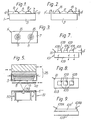
- a semiconductor device 1 comprising a monocrystalline substrate 3 of n-type doped indium antimonide (InSb) semiconductor material having two semi- conductor regions 5 formed on its upper surface 7. These regions 5 are of gray (a-phase) tin. Ohmic contacts 9, to the semiconductor regions, may be formed using pressure dots of indium. An additional ohmic contact 11 may also be provided by an indium pressure dot.
- the semiconductor regions 5 have each a trace content of an impurity dopant, e.g. boron, are each monocrystalline and, are in intimate contact with the substrate 3. They each provide thus a p-n diode junction in the region of intimate contact at the interface between the semiconductor gray tin 5 and the indium antimonide substrate 3.
- the semiconductor region 5 is of depth "d" having a thickness up to about 0.5 ⁇ m and remains in the a-phase at temperatures in excess of 13.2°C, the temperature attributed to the phase transition between the semiconducting a-phase (gray allotrope) of tin and the metallic A-phase (wh allotrope) of tin. It is found, surprisingly, that these regions of tin 5 remain, for an indefinite period, >1 1/2 years, in the semiconducting a-phase over a range of temperature exceeding 13.2°C up to an upper temperature limit of approximately 70°C. This stabilisation of the a-phase is attributed to a surface interaction between the tin and the supporting substrate.
- the thickness "d" of the semiconductor regions 5 is limited by the finite range of the surface interaction, but this can be used to advantage to provide effective ohmic contact between semiconductor (a-phase) gray tin and metal ( ⁇ -phase) white tin as shown with reference to the assembly 1' shown in figures 2 and 3 of the accompanying drawings.
- thicker deposits 13 of tin are provided in intimate contact with the monocrystalline substrate 3.
- each deposit 13 of tin is subdivided into two coexisting phase regions, a proximal region 5 which is of semiconductor a-phase gray tin and a distal region 15 of metal A-phase white tin.
- An ohmic contact to each semiconductor region 5 is thus formed at the phase interface between the proximal and distal regions of the tin deposit 13.
- a semiconductor device may then be produced from this assembly 1' by the further provision of conducting leads.
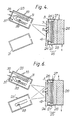
- FIG. 4 An apparatus for producing the semi- conductor device 1 or the assembly 1' is shown in figure 4.
- This apparatus includes an argon ion bombardment source 21 and a tin evaporation source, a Knudsen oven 23.
- Both the source 21 and the oven 23 are mounted in an enclosure (not shown). They are each directed at the substrate 3 which is affixed by means of clips 24 to a supporting structure 25.
- This supporting structure 25 includes a heating element having a ribbon heater 26 sandwiched between two thin silica slides 27 in contact with a stainless steel plated block 28 of high thermal capacity. This block 28 is cooled by means of a heat exchanger 29 to enable cooling of the substrate 3 under operative conditions.
- the oven 23 is principally of pyrolytic boron nitride (pBN) construction 31 and is surrounded by radiation shields 33, the innermost shields being of platinum (Pt), the outermost shields being of tantalum (Ta). Oven heating is provided by a molybdenum heater spiral 35. Oven temperature is monitored by a thermo-couple 37.
- the oven 23 has been loaded with a charge 39 of tin of very high purity ⁇ 5N ⁇ eg Cominco 6N (total impurity content better than 11 p.p.m.).
- the substrate 3 is of n-type indium antimonide, is formed of a monocrystalline slice of indium antimonide and has in this example a front surface 7 cut in the (100) plane. Alternatively, the slice may be cut in the (111)A or (111) B plane. Thus surface has been chemically cleaned.
- the substrate 3 was supplied commercially by MCP Electronics Limited, Alperton Road, Wembley, England, being supplied as chemically treated to a mirror smooth, undamaged surface finish by a proprietary process.
- the enclosure is pumped down to an ultra high vacuum ( ⁇ 10 -9 Torr).
- the substrate surface 7 is subsequently treated to remove surface impurities-eg principally of oxygen (O 2 ) and carbon (C)-that would otherwise inhibit formation of the ⁇ -phase of tin during subsequent deposit.
- the substrate 3 is bombarded by argon ions of 500 eV energy from the source 21 at a current density of 1 ⁇ A/sq cm for a cycle of 30 minutes.
- the condition of the surface can be monitored in situ by Auger electron spectroscopy and the cycles repeated until the surface is atomically clean- ie with the front monolayer of atoms including less than 1 at.% total of impurity species.
- the substrate 3 is annealed between each cycle to relieve stresses developed in the crystalline lattice and to restore crystallographic order, at a temperature of about 220°C each for a period of about 30 minutes. Following this, in situ electron diffraction is used to confirm that the substrate surface is well ordered.
- a patterned mask 41 of molybdenum or silicon is then interposed and positioned between the substrate 3 and the oven 23, and the substrate is cooled to an initial temperature of about -20°C.
- the oven 23 which initially is shuttered, is then heated to a temperature of about 1250°C so that the tin charge 39 begins to evaporate and provide tin vapour at a vapour pressure of approximately 10- 2 Torr.
- the shutter (not shown) is then removed and the substrate 3 exposed to a molecular beam of tin; through the mask 41.
- a suitable growth rate of between 0.5 ⁇ m/hour to 5 ⁇ m/hour can be achieved, the substrate temperature being held below about 70°C by cooling during this operation. This evaporation is continued until regions 5 (or 13) of tin of desired thickness are grown. Leads may then be formed in a subsequent stage of the process.
- regions of tin 5 (or 13) of defined shape may be produced by means other than the mask 41.
- the shaped regions 5 (or 13) may be shaped from an epitaxially grown monocrystalline tin film by photolithography and chemical etching or by ion beam milling of the film during subsequent process steps.
- a further advantage of the assembly 1' is that the ohmic contacts 15 are produced together with the semiconductor regions 5 during a single evaporation step. metal ⁇ -tin nucelating after a critical thickness of semiconductor ⁇ -tin (-0.5 ⁇ m) has been deposited, if evaporation is continued.
- the crystallographic structure of indium antimonide is that of the zinc blende (ZnS) structure and is isomorphous with the structure of a-phase (gray allotrope) tin, which has the structure of diamond. Also the interatomic spacing of indium antimonide-6.479A (at 18°C) is closely matched to that of a-phase tin-6.489A (at 20°C), and the match is reasonably close over a wide range of temperature.
- p-n diodes of p-type tin on n-type indium antimonide have been grown.
- the semi- conductor tin had a p-carrier concentration of ⁇ 1 to 5x10 19 cm- 3 , the carrier origin being assigned to boron from the boron nitride cells used in the evaporation.
- the Sn-InSb p-n junctions exhibited electrical rectifying behaviour with RoA values of about 1 to 10 and a measured hole mobility in the p-type ⁇ -Sn of about 200 cm2 v -1 sec -1 .
- Semiconductor tin can also be grown epitaxially in the manner described above, using instead of indium antimonide, a substrate of cadmium telluride.
- the surface can be polished by combined chemical and mechanical action using a solution of bromine in methanol, and a lower temperature can be used for the anneal treatment.
- the crystallographic structure of cadmium telluride, an insulating material is also that of the zinc-blende structure, so is also isomorphous with the structure of a-phase tin.
- the interatomic spacing is 6.840A (at 25°C) and is also closely matched to the spacing of a-phase tin.
- Cadmium telluride has a band gap of -1.5 eV, is greater than that of indium antimonide (0.18 eV) and is available in semi-insulating form at room temperature.
- semiconductor tin may be epitaxially grown on a substrate of germanium or silicon. These have the diamond crystallographic structure.
- Germanium has an interatomic spacing ⁇ 5.66 ⁇ and silicon -5.43A and are not therefor as closely matched to the interatomic spacing of a-Sn. They differ from a-Sn by approximately 12.7% and 16.3% respectively-both are matched to a-Sn within a tolerance of approximately 17% over a wide range of temperature.
- tin is deposited by means of an electron gum (e-gun) source 51 in place of the oven 23.
- tin atoms are ejected from the surface of the tin charge 39 under the bombardment of energetic electrons emitted from a cathode 53.
- Donor or acceptor impurities may be introduced from a similar auxiliary source simultaneous to ⁇ -Sn growth or during a subsequent process step.
- Substitutional impurity doping may be used to increase the thickness of the tin region 5 that may be made both semiconducting and stable.
- a second oven 23' containing a charge 59 and suitable dopant.
- evaporation of the dopant 59 may take place simultaneously, during the whole of the deposit process.
- the dopant 59 can be introduced into the tin charge 39 in the oven 23 and both tin and dopant evaporated simultaneously.
- evaporation of the dopant may be discontinued to allow further growth of pure tin and the formation of ohmic contact regions of metal A-phase tin.
- a content of between 0.75 at.% and 1.0 at.% germanium may be introduced.
- doped semi- conductor tin regions 5 have been grown up to about 1 to 2 ⁇ m thickness, which, provided the substrate temperature has been maintained at below about 70°C, have proved stable subsequently in the temperature range between 13.8°C and -70°C.
- a phase transition to metal A-phase. tin occurs and with substitutional impurity doping, as above, the regions grown have not readily reverted to the semiconductor a-phase.
- Cadmium telluride may also be grown epitaxially over the monocrystalline region 5 of a-phase gray tin. As such it serves to passivate the surface, preventing exposure of the tin to atmospheric oxygen.
- the devices produced by the above process may also be configured to perform as infra-red detecting devices.
- FIG. 7 There is shown in figures 7 and 8 a linear array of three photovoltaic detector regions 105 of semiconductor grey tin ( ⁇ -phase) formed on a monocrystalline substrate 103 of n-type doped indium antimonide semi-conductor material.
- Each region 105 has been epitaxially grown by the evaporative technique described above, each is monocrystalline and is in intimate contact with the substrate 103.
- Ohmic contacts to the semiconductor regions 105 are provided by indium pressure bonds 109, and a further ohmic contact to the semiconductor substrate 103 is provided by an indium pressure bond 111.
- Evaporated indium contact pads joined to gold or platinum leads by conducting epoxy resin may also be used for ohmit contacts to both semiconducting tin and indium antimonide.
- the indium antimonide substrate acts as a window for infra-red radiation of wavelength ⁇ greater than the indium antimonide cut-off ⁇ 5.7 ⁇ m).
- the spectral response of each photodiode, thus formed extends from 5.7 ⁇ m to 9 ⁇ m and thus extends in part to cover radiation transmitted through the 8 ⁇ m to 14 ⁇ m atmospheric infra-red window.
- Infra-red radiation in the 5.7 ⁇ m to 9 ⁇ m band falling on the detector array induces a photovoltage across each p-n junction and is measured across ohmic contact 109 and 111.
- a photoconductive device is provided by an extended strip 105' of semiconductor tin having indium pressure bonds 109A, 109B providing ohmic contact at either end of the strip 105'.
- the strip has been formed by the process described above using a suitably modified mask, and is in intimate contact with an insulating substrate of monocrystalline cadmium telluride 103.
- infra-red radiation of suitable wavelength ⁇ 9 ⁇ m
- the conductivity of the strip 105' between contacts 109A, 109B is changed by the generation of photocarriers in response to radiation absorbed in the strip 105'.
- Sandwiched layers of a-Sn and cadmium telluride may be built up to increase the effective thickness of a-Sn available to absorb infra-red radiation.
Landscapes
- Physics & Mathematics (AREA)
- Condensed Matter Physics & Semiconductors (AREA)
- General Physics & Mathematics (AREA)
- Electromagnetism (AREA)
- Optics & Photonics (AREA)
- Physical Deposition Of Substances That Are Components Of Semiconductor Devices (AREA)
- Light Receiving Elements (AREA)
Claims (10)
Applications Claiming Priority (4)
| Application Number | Priority Date | Filing Date | Title |
|---|---|---|---|
| GB8009588 | 1980-03-27 | ||
| GB8010250 | 1980-03-27 | ||
| GB8009588 | 1980-03-27 | ||
| GB8010250 | 1980-03-27 |
Publications (2)
| Publication Number | Publication Date |
|---|---|
| EP0048255A1 EP0048255A1 (de) | 1982-03-31 |
| EP0048255B1 true EP0048255B1 (de) | 1984-12-27 |
Family
ID=26274916
Family Applications (1)
| Application Number | Title | Priority Date | Filing Date |
|---|---|---|---|
| EP81900812A Expired EP0048255B1 (de) | 1980-03-27 | 1981-03-26 | Halbleitervorrichtung und deren herstellung |
Country Status (3)
| Country | Link |
|---|---|
| EP (1) | EP0048255B1 (de) |
| JP (1) | JPS57500358A (de) |
| WO (1) | WO1981002811A1 (de) |
Family Cites Families (2)
| Publication number | Priority date | Publication date | Assignee | Title |
|---|---|---|---|---|
| FR1129220A (fr) * | 1955-07-25 | 1957-01-17 | Piles photovoltaïques à rendement élevé | |
| US3615856A (en) * | 1969-04-14 | 1971-10-26 | Rca Corp | Germanium-tin alloy infrared detector |
-
1981
- 1981-03-26 JP JP56501028A patent/JPS57500358A/ja active Pending
- 1981-03-26 WO PCT/GB1981/000057 patent/WO1981002811A1/en not_active Ceased
- 1981-03-26 EP EP81900812A patent/EP0048255B1/de not_active Expired
Also Published As
| Publication number | Publication date |
|---|---|
| JPS57500358A (de) | 1982-02-25 |
| EP0048255A1 (de) | 1982-03-31 |
| WO1981002811A1 (en) | 1981-10-01 |
Similar Documents
| Publication | Publication Date | Title |
|---|---|---|
| US6657194B2 (en) | Multispectral monolithic infrared focal plane array detectors | |
| KR100224553B1 (ko) | 솔라 셀 및 이의 제조 방법 | |
| JP2004119525A (ja) | 酸化物半導体pn接合デバイス | |
| US20030102432A1 (en) | Monolithic infrared focal plane array detectors | |
| US4650921A (en) | Thin film cadmium telluride solar cell | |
| EP0612112B1 (de) | Verfahren zur Herstellung einer chalkopyrit-Halbleiterschicht | |
| US4734381A (en) | Method of making a thin film cadmium telluride solar cell | |
| US11851785B2 (en) | Aluminum nitride passivation layer for mercury cadmium telluride in an electrical device | |
| US4468685A (en) | Infrared detector using grey tin | |
| US5608208A (en) | Single layer planar HgCdTe photovoltaic infrared detector with heterostructure passivation and p-on-n homojunction | |
| US4004342A (en) | Fabrication of ion implanted P-N junction devices | |
| US4089714A (en) | Doping mercury cadmium telluride with aluminum or silicon | |
| Suda et al. | Zn3P2/ITO heterojunction solar cells | |
| CN103460340A (zh) | 用于形成适合用于微电子器件的磷属元素化物组合物的方法 | |
| US4087293A (en) | Silicon as donor dopant in Hg1-x Cdx Te | |
| JPS6248390B2 (de) | ||
| US4086106A (en) | Halogen-doped Hg,Cd,Te | |
| JP3181074B2 (ja) | Cu系カルコパイライト膜の製造方法 | |
| WO1981002811A1 (en) | A semiconductor device and the manufacture thereof | |
| GB2077489A (en) | A semiconductor device of grey tin and the manufacture thereof | |
| Livingstone et al. | Si/CdS heterojunction solar cells | |
| Cohen-Solal et al. | Structure and Properties of CdxHg1-xTe Films | |
| Kumar et al. | Liquid Encapsulated Czochralski Growth of Large size Gallium Arsenide and Indium Phosphide Single Crystals and their Characterisation—A Review | |
| Kohiki et al. | CuInSe2 homojunction diode fabricated by phosphorus doping | |
| Hill | Cadmium-sulphide/copper-sulphide thin-film solar cells: review of methods of producing the CdS and Cu2S layers |
Legal Events
| Date | Code | Title | Description |
|---|---|---|---|
| PUAI | Public reference made under article 153(3) epc to a published international application that has entered the european phase |
Free format text: ORIGINAL CODE: 0009012 |
|
| 17P | Request for examination filed |
Effective date: 19811105 |
|
| AK | Designated contracting states |
Designated state(s): DE FR NL |
|
| RAP1 | Party data changed (applicant data changed or rights of an application transferred) |
Owner name: THE SECRETARY OF STATE FOR DEFENCE IN HER BRITANNI |
|
| GRAA | (expected) grant |
Free format text: ORIGINAL CODE: 0009210 |
|
| AK | Designated contracting states |
Designated state(s): DE FR NL |
|
| REF | Corresponds to: |
Ref document number: 3167901 Country of ref document: DE Date of ref document: 19850207 |
|
| ET | Fr: translation filed | ||
| PLBE | No opposition filed within time limit |
Free format text: ORIGINAL CODE: 0009261 |
|
| STAA | Information on the status of an ep patent application or granted ep patent |
Free format text: STATUS: NO OPPOSITION FILED WITHIN TIME LIMIT |
|
| 26N | No opposition filed | ||
| PGFP | Annual fee paid to national office [announced via postgrant information from national office to epo] |
Ref country code: NL Payment date: 19860331 Year of fee payment: 6 |
|
| PG25 | Lapsed in a contracting state [announced via postgrant information from national office to epo] |
Ref country code: NL Effective date: 19871001 |
|
| NLV4 | Nl: lapsed or anulled due to non-payment of the annual fee | ||
| PG25 | Lapsed in a contracting state [announced via postgrant information from national office to epo] |
Ref country code: FR Free format text: LAPSE BECAUSE OF NON-PAYMENT OF DUE FEES Effective date: 19871130 |
|
| PG25 | Lapsed in a contracting state [announced via postgrant information from national office to epo] |
Ref country code: DE Effective date: 19871201 |
|
| REG | Reference to a national code |
Ref country code: FR Ref legal event code: ST |