EP0048896B1 - Circuit pour la génération d'un signal de synchronisation d'horloge - Google Patents
Circuit pour la génération d'un signal de synchronisation d'horloge Download PDFInfo
- Publication number
- EP0048896B1 EP0048896B1 EP81107326A EP81107326A EP0048896B1 EP 0048896 B1 EP0048896 B1 EP 0048896B1 EP 81107326 A EP81107326 A EP 81107326A EP 81107326 A EP81107326 A EP 81107326A EP 0048896 B1 EP0048896 B1 EP 0048896B1
- Authority
- EP
- European Patent Office
- Prior art keywords
- signal
- circuit
- counting
- clock
- scale
- Prior art date
- Legal status (The legal status is an assumption and is not a legal conclusion. Google has not performed a legal analysis and makes no representation as to the accuracy of the status listed.)
- Expired
Links
Images


Classifications
-
- H—ELECTRICITY
- H04—ELECTRIC COMMUNICATION TECHNIQUE
- H04L—TRANSMISSION OF DIGITAL INFORMATION, e.g. TELEGRAPHIC COMMUNICATION
- H04L7/00—Arrangements for synchronising receiver with transmitter
- H04L7/02—Speed or phase control by the received code signals, the signals containing no special synchronisation information
- H04L7/033—Speed or phase control by the received code signals, the signals containing no special synchronisation information using the transitions of the received signal to control the phase of the synchronising-signal-generating means, e.g. using a phase-locked loop
- H04L7/0331—Speed or phase control by the received code signals, the signals containing no special synchronisation information using the transitions of the received signal to control the phase of the synchronising-signal-generating means, e.g. using a phase-locked loop with a digital phase-locked loop [PLL] processing binary samples, e.g. add/subtract logic for correction of receiver clock
Definitions
- the present invention relates to a clock synchronization signal generating circuit according to the pre-characterizing portion of any one of claims 1, 21, 22, 25 or 28 for achieving clock synchronization between digital operation systems such as data modems.
- the frequency variable oscillator circuit of digital type is often used instead of analog VCO.
- the digital frequency variable oscillator circuit can not change the instantaneous frequency continuously and is intended to accord in frequency the clock signal in the slave system with that in the master system by extracting or inserting one clock pulse from or into the clock output signal for every constant time period.
- the data modem of synchronization type has the transmitting section which operates as master unit and the receiving section which operates as slave unit, and can carry out master and slave operations simultaneously or selectively. It is advantageous in this data modem of synchronization type that as may circuits as possible are designed to be used commonly in master and slave units. It is also advantageous that master and slave units in the data modem are driven by the same clock signal. However, as will be later described in detail referring to Figs. 1 and 2, it is necessary in the conventional clock synchronizing method that a specific clock generator is arranged in master and slave units in each operation system for the purpose of selectively operating two operation systems in master and slave modes and always clock-synchronizing the slave system with the master system.
- phase locked loop circuit is described in "Electrical Design News", Vol. 17, Nr. 6, 15. March 1972, pages 36-39. Also in this known circuit a counter is provided in which different divisions can be selected. However, this known circuit is only provided for operating in a receiving mode.
- the object of the present invention is to provide a clock synchronization signal generating circuit of the kind as initially indicated capable of achieving good clock synchronizing operation between digital operation systems even when digital operation systems operate as master or slave system, whereby synchronization is simplified when switching between master and slave modes.
- first digital operation system which is set to master mode is clock-synchronized with that of second digital operation system which is set to slave mode
- an input signal in synchronism with a signal obtained by dividing the frequency of a first source clock signal by a frequency dividing factor of (N + 1) is supplied from the clock circuit in the first digital operation system to the clock synchronizing circuit in the second digital operation system.
- the clock synchronizing circuit in the second digital operation system is controlled so as to selectively frequency-divide a second source clock signal by a frequency dividing factor of N or (N + 2), for example, according to the phase difference between the input clock signal and the second source clock signal.
- a relation of N ⁇ (N + 1) ⁇ (N + 2) is thus obtained and the operation of second digital operation system can be excellently clock-synchronized with that of first digital operation system by setting the frequency of first source clock signal substantially equal to that of second source clock signal.
- clock signal by selectively frequency dividing factors of N and (N + 1), for example, or by frequency dividing the first source clock signal substantially by a frequency dividing factor of (N + M) wherein 0 ⁇ M ⁇ 1 is supplied from the clock circuit in the first digital operation system which is set to master mode to the clock synchronizing circuit in the second digital operation system which is set to slave mode.
- the clock synchronizing circuit in the second digital operation system is controlled so as to selectively frequency-divide the second source clock signal by the dividing factor of N or (N + 1), for example, according to the phase difference between the input clock signal and the second source clock signal.
- a relation of N ⁇ (N + M) ⁇ (N + 1) is thus obtained and the operation of second digital operation system can be excellently clock-synchronized with that of first digital operation system by setting the frequency of first source clock signal substantially equal to that of second source clock signal.
- Fig. 1 shows a conventional clock synchronizing circuit of digital type which is formed as a phase locked loop.
- This clock synchronizing circuit includes a phase comparator 2 for comparing phases of input signals, a clock control circuit 4 for controlling, responsive to an output signal from the phase comparator 2, the clock signal from a clock signal generator 6, and a quaternary or four-scale counter 8 for counting an output signal from the clock control circuit 4 and producing an output signal of high level when it takes one of four counting values "0" to "3", for example, a counting value "0".
- the clock signal generator 6 generates a source clock signal shown in Fig. 2(A).
- the phase comparator 2 compares an input clock signal supplied from the master system and shown in Fig. 2(B) with an output clock signal generated through the counter 8 and shown in Fig. 2(C), for example, and generates an output pulse signal shown in Fig. 2(D) when clock signals shown in Figs. 2(B) and 2(C) are of low and high levels, respectively.
- the clock control circuit 4 extracts a pulse which will be next generated from the clock signal generator 6 responsive to an output pulse supplied from the phase comparator 2 and generates a pulse signal shown in Fig. 2(E).
- the counter 8 counts output pulses from the clock control circuit 4 and generates a high level signal shown in Fig.
- the variable range of frequency f ; of input clock signal is determined by a constant frequency f c of source clock signal from the clock signal generator 6.
- the frequency f, of input clock signal is variable in a range shown by the following expression:
- a first operation system which uses a source clock signal of frequency f c1 as reference timing signal used for processing operation is operated as master system and a second operation system which uses a source clock signal of frequency f C2 is operated as slave system.
- the master system carries out one cycle processing operation at every predetermined number of reference clock pulses or every four clock pulses, for example, and supplies the clock signal shown in Fig. 2(B) to the slave system.
- the second operation system is operated as master system and the first operation system as slave system, it is required that the following condition is satisfied to clock-synchronize the input signal (fci4) supplied to the slave system with the source clock signal (f ei ) employed in the slave system:
- Fig. 3 shows a digital operation system using a clock synchronization signal generating circuit of the present invention.
- the clock synchronization signal generating circuit includes a clock pulse generator 10, a clock synchronizing circuit 12 and a clock circuit 14 both supplying, responsive to a clock pulse signal from the clock pulse generator 10, a clock synchronizing signal and clock signal to a data processing unit 16 as timing signals.
- a control clock signal is supplied from the clock circuit 14 to the data processing unit 16 to render the digital operation system operative in master mode and a control clock signal is supplied from the clock synchronizing circuit 12 to the data processing unit 16 to render the digital operation system operative in slave mode.
- the clock synchronizing circuit 12 includes a scale variable counter 20 for counting clock pulses from the clock pulse generator 10, a control circuit 22 for controlling the scale variable counter 20 in such a way that a clock signal in synchronism with the source clock signal employed in another digital operation system operating in master mode is accorded in frequency with an output signal of scale variable counter 20, and a decoder 24 for decoding the output signal of scale variable counter 20 to supply it to the data processing unit 16 as control clock signal.
- the clock circuit 14 includes a counter 40 for counting clock pulses from the clock pulse generator 10, and a decoder 42 for decoding the output signal of counter 40 to supply it to the data processing unit 16 as control clock signal.
- the digital operation system shown in Fig. 3 can be used as full duplex modem where the data processing unit has the master (modulation) section and slave (demodulation) section separately. Namely, the digital operation system can be operated in master-slave mode responsive to control clock signals applied from decoders 24 and 42. However, in the case of digital operation system operating selectively in master or slave mode as in the half-duplex modem, the counter 40 and decoder 42 can be omitted as shown in Fig. 4.
- a clock synchronization signal generating circuit 13 employed in the digital operation system of Fig. 4 is substantially the same in arrangement as the one shown in Fig.
- control circuit 23 whose operation is determined responsive to master-slave mode selection signals produced from a master-slave mode selection circuit 18 is used instead of control circuit 22.
- the digital operation system operates in master mode, for example, the operation of control circuit 23 is stopped responsive to the mode selection signal produced from the mode selection circuit 18, so that the counter 20 may carry out counting operation without changing its scale.
- the control circuit 23 is rendered operative responsive to the mode selection signal produced from the mode selection circuit 18, so that the scale of counter 20 can be changed according to the control signal supplied from the control circuit 23.
- mode selection signals are generated through the mode selection circuit 18, but may be generated through the data processing unit 16 according to the programming operation of data processing unit 16 in the digital operation system.
- Fig. 5 shows a detailed circuit diagram of scale variable counter 20 and control circuit 22 in the clock synchronizing circuit 12 shown in Fig. 3.
- the scale variable counter 20 has J-K flip-flop circuits 200, 202 and 204 which receive through their clock terminals a source clock signal generated from the clock pulse generator 10.
- the K input terminal of the flip-flop circuit 200 is connected to receive a "1" level signal the Q output terminal, thereof to first input terminals of AND gates 206 and 208, and the Q output terminal thereof to first input terminals of a NAND gate 210 and an AND gate 212.
- J and K input terminals of the flip-flop circuit 202 are connected to the output terminal of AND gate 206, and the Q output terminal thereof to second input terminals of AND gates 208 and 212.
- the J input terminal of flip-flop 204 is connected to the output terminal of AND gate 208, the K input terminal thereof to the output terminal of an AND gate 214 whose first input terminal is connected to the outer terminal of NAND gate 210, the Q output terminal thereof to the second input terminal of AND gate 214 and to the first input terminal of NAND gate 216 whose output terminal is connected to the J input terminal of flip-flop circuit 200, and the Q output terminal thereof to the second input terminal of AND gate 206.
- the control circuit 22 has the D-type flip-flop circuit 220 which receives through its clock terminal the source clock signal applied from the clock pulse generator 10, a D-type flip-flop circuit 222 whose clock terminal receives via an inverter 224 the source clock signal, AND gates 226 and 228 whose first input terminals are connected to the output terminal of AND gate 212 in the counter 20, and AND gates 230 and 232 whose first input terminals are connected via an inverter 234 to the output terminal of AND gate 212.
- the D input terminal of flip-flop circuit 220 is connected to the output terminal of an OR gate 236 which is connected to output terminals of AND gates 226 and 230, and the Q output terminal thereof to first input terminals of AND gates 238 and 240 and to the second input terminal of AND gate 230.
- Output terminals of AND gates 238 and 240 are connected to second input terminals of NAND gates 210 and 216, respectively, and to the input terminals of an OR gate 242.
- the output terminal of OR gate 242 is connected to the third input terminal of AND gate 208 in the counter 20.
- the D input terminal of flip-flop circuit 222 is connected to the output terminal of an OR gate 244 which is connected to output terminals of AND gates 228 and 232, the Q output terminal thereof to second input terminals of AND gates 232 and 238, and the Q output terminal thereof to the second input terminal of AND gate 240.
- OR gate 244 which is connected to output terminals of AND gates 228 and 232, the Q output terminal thereof to second input terminals of AND gates 232 and 238, and the Q output terminal thereof to the second input terminal of AND gate 240.
- To second input terminals of AND gates 226 and 228 is supplied an input clock signal in synchronism with the source clock signal used in a different operation system which operates in master mode.
- the operating mode of counter 20 is determined responsive to output signals supplied from AND gates 238, 240 and OR gate 242 in the control circuit 22. Namely, the counter 20 operates as a 6- scale counter or 1 ⁇ 4 frequency divider when the output signal of AND gate 238 is at a level "1", as a 5-scale counter or V 5 frequency divider when the output signal of AND gate 240 is at a level "1”, and as a 4-scale counter or /• frequency divider when output signals of AND gates 238 and 240 are at a level "0".
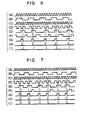
- Fig. 6(A) shows a source control clock signal used in the different digital operation system
- Fig. 6(B) an input clock signal synchronized with the source clock signal shown in Fig. 6(A) and supplied to the control circuit 22
- Fig. 6(C) a source clock signal generated through the clock pulse generator 10 (Fig. 3).
- the source clock signal generated through the clock pulse generator 10 has a higher frequency than the source clock signal used in the different digital operation system.
- the counter 40 of clock circuit 14 in each of digital operation systems operates as a quinary or 5-scale counter.
- the flip-flop circuit 220 Only when a high level output signal is generated through the AND gate 212 and the input clock signal [Fig. 6(B)] is at a low level, the flip-flop circuit 220 produces a Q output signal of low level in response to the leading edge of source clock pulse. It is when a high level output signal is generated through the AND gate 212 and the leading edge of source clock pulse is supplied to the flip-flop circuit 220 in the case where the input clock signal is in high level that the output state of flip-flop circuit 220 is changed from level "0" to level "1".
- the output state of flip-flop circuit 220 is set at a high or low level responsive to the high or low level of input clock signal at a timing shown in Fig. 6(H) and the output state of flip-flop circuit 222 is set at a high or low level responsive to the high or low level of input clock signal at a timing shown in Fig. 6(1) in each counting cycle. Therefore, when it is detected that input clock signals shown in Fig. 6(B) are both at a high level at timings shown in Figs. 6(H) and 6(1), the counter 20 is set to operate as a 6-scale counter, when it is detected that input clock signals are at high and low levels, respectively, at timings shown in Figs.
- the counter 20 is set to operate as a 5-scale counter, and when it is detected that input clock signals are at a low level at timings shown in Figs. 6(H) and 6(1), the counter 20 is set to operate as a 4-scale counter. The level of input clock signal is detected at timings shown in Figs. 6(H) and 6(1) every counting cycle as described above and the counting scale in a following counting cycle is determined according to the detected result.
- the scale variable counter 20 will be selectively set to operate in 5- or 6-scale counting mode responsive to the control signal supplied from the control circuit 22, thus supplying an output signal through flip-flop circuits 200, 202 and 204 to the decoder 24.
- the decoder 24 supplies to the data processing unit 16 an output clock signal defined by the output signal from the counter 20 and clock-synchronized with the input clock signal.
- Fig. 7 shows a case where the input clock signal shown in Fig. 7(B) which is obtained by dividing by 5 the frequency of source clock signal shown in Fig. 7(A) and having a higher frequency than that of source clock signal supplied from the clock pulse generator 10 as shown in Fig. 7(C) is supplied to the control circuit 22.
- Figs. 7(A) to 7(1) correspond to Fig. 6(A) to 6(1). Therefore, the scale variable counter 20 is selectively set to operate in 5- or 4-scale counting mode responsive to the control signal from the control circuit 55 in this case, thus supplying an output signal through flip-flop circuits 200, 202 and 204 to the decoder 24.
- the counter 20 and control circuit 22 shown in Fig. 5 can be employed in the clock synchronization signal generating circuit shown in Fig. 4.
- the mode selector 18 may be connected to the control circuit 22 in such a way that a signal of level "1" from the mode selector 18 is supplied to the OR gate 236 and a signal of level "0" to AND gates 228 and 232.
- Q output signals of flip-flop circuits 220 and 222 are set at high and low levels, respectively, and the counter 20 fixedly operates as a 5-scale counter.
- a signal of level "0" is supplied to the OR gate 236 while a signal of level “1” to AND gates 228 and 232, and the counter 20 is selectively set, as described above, to operate as a 4-, 5- or 6-scale counter according to a control signal from the control circuit 22.
- Fig. 8 shows a clock synchronizing circuit in a clock synchronization signal generating circuit which is another embodiment of the present invention.
- the clock synchronizing circuit includes a 4-scale counter 30, a control circuit 32 whose arrangement is the same as that of control circuit 22 shown in Fig. 5, and a clock control circuit 34 for changing the frequency of source clock signal responsive to an output signal of control circuit 32.
- the 4-scale counter 30 includes J-K flip-flop circuits 300, 302, an AND gate 304 connected to Q output terminals of flip-flop circuits 300, 302, and AND gate 306 connected to the Q output terminal of flip-flop circuit 300 and to the Q output terminal of flip-flop circuit 302, and an AND gate 308 which receives the source clock signal through an input terminal and whose output terminal is connected to clock input terminals of flip-flop circuits 300, 302.
- the control circuit 32 generates through AND gates 238 and 240 an output signal corresponding to the level of input clock signal in response to trailing and leading edges of a source clock signal while a high level signal is being generated through the AND gate 306.
- the clock control circuit 34 includes AND gates 340 and 342 whose first input terminals are connected to output terminals of AND gates 238 and 240, respectively, monostable multivibrators 344 and 346 connected to output terminals of AND gates 340 and 342, and a monostable multivibrator 348 connected to the output terminal of AND gate 304.
- To second input terminals of AND gates 340 and 342 is supplied a source clock signal through an inverter 350 and to third input terminals thereof an output signal of monostable multivibrator 340.
- Output signals of monostable multivibrators 344 and 346 are supplied through a NOR gate 352 to the other input terminal of AND gate 308.
- an input clock signal supplied to the control circuit 32 is a clock signal obtained by dividing by 5 a source clock signal (not shown) employed in a different operation system.
- Q output signals of flip-flop circuits 300 and 302 are set at levels "0" and "1", respectively, and levels of the input clock signal' at timings at which trailing and leading edges of the source clock signal are generated at this time are detected to be at a level "0".
- signal of low level is generated through AND gates 238 and 240, so that a signal of level "1" is generated through the NOR gate 352.
- To the counter 30 is therefore supplied the source clock signal shown in Fig. 9(A).
- the inverted signal of source clock signal triggers monostable multivibrators 344 and 346 through AND gates 340 and 342 causing these monostable multivibrators 344 and 346 to generate high level signals over predetermined periods of time.
- the signal shown in Fig. 9(D) is thus supplied from the NOR gate 352 to the AND gate 308.
- every fifth and sixth clock pulses in the source clock signal are removed and the clock signal shown in Fig. 9(E) is supplied to the counter 30.
- the monostable multivibrator 348 produces a "1" level signal in response to the leading edge of a "1" level output signal from the AND gate 304 for a time substantially equal to one period of time of the source clock signal so as to define the timing at which monostable multivibrators 344 and 346 can be triggered.
- the counter 30 and control circuit 32 shown in Fig. 8 can be employed in the clock synchronization signal generating circuit shown in Fig. 4.
- the mode selector 18 may be connected to the control circuit 32, as shown by the broken line in Fig. 5, in such a way that the signal of level "1" from the master-slave mode selector 18 is supplied to the OR gate 236 and the signal of level "0" to AND gates 228 and 232.
- Q output signals of flip-flop circuits 220 and 222 are set at levels "1" and "0", respectively, the control signal shown in Fig.
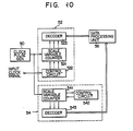
- Fig. 10 shows a clock synchronization signal generating circuit which is a further embodiment of the present invention.
- the clock synchronization signal generating circuit includes a clock pulse generator 50, and a clock synchronizing circuit 52 and a clock circuit 54 which respectively supply, in response to a clock pulse signal from the clock pulse generator 50, clock synchronizing signal and clock signal to a data processing unit 56 as timing signals.
- the clock synchronizing circuit 52 includes a scale variable counter 521 for counting clock pulses from the clock pulse generator 50, a control circuit 522 for controlling the scale variable counter 521 and such a way that a clock signal in synchronism with the source clock signal employed in the digital operation system operating in master mode is matched in frequency with the output signal of scale variable counter 521, and a decoder 523 for decoding the output signal of scale variable counter 521 to supply the control clock signal to the data processing unit 56.
- the clock circuit 54 includes a scale variable counter 541 for counting source clock pulses from the clock pulse generator 50, a control circuit 542 for controlling the scale of scale variable counter 541, and a decoder 543 for decoding the output signal of counter 541 to supply it to the data processing unit 56 as control clock signal.
- the scale variable counter 521 When the scale variable counter 521 is selectively controlled by the control circuit 522 to operate in 4- or 5-scale counting mode in this embodiment, for example, the scale variable counter 541 can be operated in 4- or 5-scale counting mode responsive to a control signal from the control circuit 542.
- Fig. 11 shows a detailed circuit diagram of scale variable counter 521 and control circuit 522 in the clock synchronizing circuit 52 shown in Fig. 10.
- the scale variable counter 521 includes J-K flip-flop circuits 525 to 527 which are driven by the source clock signal.
- the Q output terminal of flip-flop circuit 525 is connected to J and K input terminals of flip-flop circuit 526 and to first input terminals of AND gates 528 and 529.
- the Q and Q output terminals of flip-flop circuit 526 are connected to second input terminals of AND gates 528 and 529, respectively.
- the Q output terminal of flip-flop circuit 527 is connected to the K input terminal thereof and to the first input terminal of a NAND gate '530 whose input terminal is connected to the J input terminal of flip-flop circuit 525, and the J input terminal thereof to the output terminal of AND gate 528.
- the control circuit 522 has a D-type flip-flop circuit 531 which is driven by a source clock signal, and an AND gate 532 which receives the input clock signal at its first input terminal.
- the Q output terminal of flip-flop circuit 531 is connected to the first input terminal of an AND gate 533 and to the third input terminal of AND gate 528 and to the second input terminal of NAND gate 530 in the counter 521.
- the second input terminal of AND gate 532 is connected to the output terminal of AND gate 529 and the second input terminal of AND gate 533 to the output terminal of AND gate 529 via an inverter 534. Output terminals of these AND gates 532 and 533 are connected to the D input terminal of flip-flop circuit 531 via an OR gate 535.
- the counter 521 counts the source clock signal shown in Fig. 12(A) in 4-scale counting mode when a low level signal is generated through the control circuit 522 but counts it in 5-scale counting mode when a high level signal is generated through the control circuit 522.
- the level of input clock signal is checked one time in each counting cycle under 4- or 5-scale counting mode, and the counting scale in a following counting cycle is determined according to the level detected.
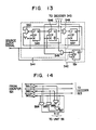
- Fig. 13 shows a detailed circuit diagram of scale variable counter 541 and control circuit 542 in the clock circuit shown in Fig. 10.
- the scale variable counter 541 is arranged similarly to the counter 521 shown in Fig. 11 and includes flip-flop circuits 545 to 547 corresponding to the circuits 525 to 527 and AND gates 548, 549 and a NAND gate 550 corresponding to those gates 528, 529 and 530.
- the control circuit 542 includes a J-K flip-flop circuit 551 whose J and K input terminals are connected to the output terminal of AND gate 549 and whose Q output terminal to input terminals of AND gate 548 and NAND gate 550.
- the counter 541 operates selectively in 4- or 5-scale counting mode according to the level of Q output signal from the flip-flop circuit 551.
- the flip-flop circuit 551 inverts the level of Q output signal in response to the source clock pulse while Q output signals of high and low levels are being generated from the flip-flop circuits 545 and 546, respectively.
- the counting mode of counter 541 is thus changed to either 4-or 5-scale counting mode in every counting cycle, so that an output signal corresponding to a frequency-divided signal obtained by dividing the frequency of source clock signal substantially by 4.5 is supplied from the counter 541 to the decoder 543.
- Fig. 14 shows a circuit section of part of a decoder designed to meet this requirement.
- the circuit section includes inverters 561 to 563 connected to Q output terminals of flip-flop circuits 525 to 527 in the counter 521, and AND gate 564 having input terminals connected to output terminals of inverters 561 to 563, and AND gate 565 connected to output terminals of inverters 562 and 563, a NAND gate 566 connected to output terminals of inverters 561 and 562, and an AND gate 567 connected to output terminals of NAND gate 566 and inverter 563.
- Output signals of the circuit section are derived out from output terminals of AND gates 564, 565, 567 and inverter 563.
- the scale variable counter 20, 521 or 541 operates in 4-, 5- or 6-scale counting mode, but more timing pulses are practically needed in one data processing cycle in the digital operation system. Therefore, it can be arranged that these counters are selectively set to operate in 256-scale, 257- scale or 258-scale counting mode, for example.
- the average value of scales of counter 541 in the clock circuit 54 is set to be larger than 4 but smaller than 5 in embodiments shown in Figs. 10 to 13 and the counter 541 is therefore controlled to operate in 4- or 5-scale counting mode.
- the counter 541 may be controlled to operate in 4- or 6-scale counting mode, for example. After the counter 541 is operated in 4-scale counting mode over four counting cycles, for example, it is operated in 6-scale counting mode in one counting cycle, thus allowing counting operation to be carried out substantially in 4.4-scale counting mode so as to achieve good clock synchronization.
- clock synchronizing circuit 52 and clock circuit 54 of Fig. 10 can be combined to form a clock synchronization signal generating circuit which can be selectively set in master or slave mode by a master-slave mode selector as explained in Fig. 4.
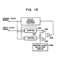
- the scale variable counters 521 and 541 are the same in construction and the control circuits 522 and 542 are different from each other. Therefore, it is possible to use the scale variable counter 521, for example, and couple the control circuits 522 and 542 to the scale variable counter 521 as shown in Fig. 15.
- output terminals of the control circuits 522 and 542 are connected to AND gates 580 and 582 whose output terminals are connected to the scale variable counter 521 through an OR gate 584.
- the AND gates 580 and 582 are controlled in response to a mode selection signal from a master-slave mode selector 586 so that output signals from the control circuits 522 and 542 are made invalid and valid, respectively, in master mode, and valid and invalid, respectively, in slave mode.
Landscapes
- Engineering & Computer Science (AREA)
- Computer Networks & Wireless Communication (AREA)
- Signal Processing (AREA)
- Synchronisation In Digital Transmission Systems (AREA)
- Stabilization Of Oscillater, Synchronisation, Frequency Synthesizers (AREA)
Claims (29)
Applications Claiming Priority (6)
| Application Number | Priority Date | Filing Date | Title |
|---|---|---|---|
| JP55133563A JPS5758435A (en) | 1980-09-25 | 1980-09-25 | Clock synchronizing system |
| JP55133562A JPS5758434A (en) | 1980-09-25 | 1980-09-25 | Clock synchronizing circuit |
| JP55133561A JPS5758433A (en) | 1980-09-25 | 1980-09-25 | Clock synchronizing system |
| JP133563/80 | 1980-09-25 | ||
| JP133561/80 | 1980-09-25 | ||
| JP133562/80 | 1980-09-25 |
Publications (3)
| Publication Number | Publication Date |
|---|---|
| EP0048896A2 EP0048896A2 (fr) | 1982-04-07 |
| EP0048896A3 EP0048896A3 (en) | 1983-02-02 |
| EP0048896B1 true EP0048896B1 (fr) | 1985-12-27 |
Family
ID=27316721
Family Applications (1)
| Application Number | Title | Priority Date | Filing Date |
|---|---|---|---|
| EP81107326A Expired EP0048896B1 (fr) | 1980-09-25 | 1981-09-16 | Circuit pour la génération d'un signal de synchronisation d'horloge |
Country Status (4)
| Country | Link |
|---|---|
| US (1) | US4475085A (fr) |
| EP (1) | EP0048896B1 (fr) |
| CA (1) | CA1183579A (fr) |
| DE (1) | DE3173313D1 (fr) |
Families Citing this family (20)
| Publication number | Priority date | Publication date | Assignee | Title |
|---|---|---|---|---|
| US4562402A (en) * | 1983-04-29 | 1985-12-31 | Tektronix, Inc. | Method and apparatus for generating phase locked digital clock signals |
| US4725944A (en) * | 1983-11-14 | 1988-02-16 | Tandem Computers Incorporated | Electronic communication clocking mechanism |
| JPS60170949A (ja) | 1984-02-15 | 1985-09-04 | Advantest Corp | マルチクロツク発生装置 |
| US4560939A (en) * | 1984-04-02 | 1985-12-24 | Sperry Corporation | Synchronized selectable rate clocking system |
| US4644195A (en) * | 1984-07-20 | 1987-02-17 | Sperry Corporation | Quad multi-channel synthesizer |
| US5118975A (en) * | 1990-03-05 | 1992-06-02 | Thinking Machines Corporation | Digital clock buffer circuit providing controllable delay |
| JPH04373009A (ja) * | 1991-06-21 | 1992-12-25 | Hitachi Ltd | クロック信号の位相調整方法及び電子装置 |
| US5272390A (en) * | 1991-09-23 | 1993-12-21 | Digital Equipment Corporation | Method and apparatus for clock skew reduction through absolute delay regulation |
| US5428764A (en) * | 1992-04-24 | 1995-06-27 | Digital Equipment Corporation | System for radial clock distribution and skew regulation for synchronous clocking of components of a computing system |
| FR2708160B1 (fr) * | 1993-07-22 | 1995-09-08 | Sagem | Système électronique à recalage d'horloge. |
| JP3468592B2 (ja) * | 1994-08-10 | 2003-11-17 | 富士通株式会社 | クロック信号発生回路 |
| US5517147A (en) * | 1994-11-17 | 1996-05-14 | Unisys Corporation | Multiple-phase clock signal generator for integrated circuits, comprising PLL, counter, and logic circuits |
| US5731728A (en) * | 1995-11-13 | 1998-03-24 | National Semiconductor Corporation | Digital modulated clock circuit for reducing EMI spectral density |
| GB9608819D0 (en) * | 1996-04-30 | 1996-07-03 | Switched Reluctance Drives Ltd | Demodulator for a pulse width modulated signal |
| US7515646B2 (en) * | 2004-02-05 | 2009-04-07 | Lexmark International, Inc. | Method and apparatus for reducing EMI emissions for data signals traveling over a data pathway |
| US20050249025A1 (en) * | 2004-04-27 | 2005-11-10 | Via Technologies, Inc. | Method and System For A Variable Frequency SDRAM Controller |
| US8514999B2 (en) * | 2011-12-06 | 2013-08-20 | International Business Machines Corporation | Floating-point event counters with automatic prescaling |
| KR102623542B1 (ko) | 2016-10-07 | 2024-01-10 | 삼성전자주식회사 | 멀티플 클럭 도메인 메모리 장치의 클럭 동기화 방법 |
| WO2019083948A2 (fr) * | 2017-10-24 | 2019-05-02 | Skywave Networks Llc | Synchronisation d'horloge lors d'une commutation entre des modes de transmission de diffusion et de données |
| CN112865899B (zh) * | 2019-11-26 | 2022-07-22 | 华为技术有限公司 | 一种调整物理层phy主从模式的方法及装置 |
Family Cites Families (12)
| Publication number | Priority date | Publication date | Assignee | Title |
|---|---|---|---|---|
| US3317843A (en) * | 1966-02-01 | 1967-05-02 | Martin Marietta Corp | Programmable frequency divider employing two cross-coupled monostable multivibratorscoupled to respective inputs of a bistable multivibrator |
| JPS4941706B1 (fr) * | 1968-08-23 | 1974-11-11 | ||
| JPS5521511B2 (fr) * | 1972-06-23 | 1980-06-10 | ||
| US3893033A (en) * | 1974-05-02 | 1975-07-01 | Honeywell Inf Systems | Apparatus for producing timing signals that are synchronized with asynchronous data signals |
| US4059842A (en) * | 1975-10-31 | 1977-11-22 | Westinghouse Electric Corporation | Method and apparatus for synchronizing a digital divider chain with a low frequency pulse train |
| US3983498A (en) * | 1975-11-13 | 1976-09-28 | Motorola, Inc. | Digital phase lock loop |
| US4012598A (en) * | 1976-01-14 | 1977-03-15 | Bell Telephone Laboratories, Incorporated | Method and means for pulse receiver synchronization |
| US4242639A (en) * | 1978-09-05 | 1980-12-30 | Ncr Corporation | Digital phase lock circuit |
| FR2448257A1 (fr) * | 1979-02-05 | 1980-08-29 | Trt Telecom Radio Electr | Dispositif de resynchronisation rapide d'une horloge |
| US4241408A (en) * | 1979-04-04 | 1980-12-23 | Norlin Industries, Inc. | High resolution fractional divider |
| US4255793A (en) * | 1979-06-11 | 1981-03-10 | The United States Of America As Represented By The United States Department Of Energy | Apparatus for generating nonlinear pulse patterns |
| NL183214C (nl) * | 1980-01-31 | 1988-08-16 | Philips Nv | Inrichting voor het synchroniseren van de fase van een lokaal opgewekt kloksignaal met de fase van een ingangssignaal. |
-
1981
- 1981-09-16 EP EP81107326A patent/EP0048896B1/fr not_active Expired
- 1981-09-16 DE DE8181107326T patent/DE3173313D1/de not_active Expired
- 1981-09-25 US US06/305,712 patent/US4475085A/en not_active Expired - Lifetime
- 1981-09-25 CA CA000386657A patent/CA1183579A/fr not_active Expired
Also Published As
| Publication number | Publication date |
|---|---|
| CA1183579A (fr) | 1985-03-05 |
| DE3173313D1 (en) | 1986-02-06 |
| EP0048896A2 (fr) | 1982-04-07 |
| US4475085A (en) | 1984-10-02 |
| EP0048896A3 (en) | 1983-02-02 |
Similar Documents
| Publication | Publication Date | Title |
|---|---|---|
| EP0048896B1 (fr) | Circuit pour la génération d'un signal de synchronisation d'horloge | |
| US4853653A (en) | Multiple input clock selector | |
| US4423383A (en) | Programmable multiple frequency ratio synchronous clock signal generator circuit and method | |
| GB2079999A (en) | Digital frequency divider | |
| US4105979A (en) | Clock regenerator comprising a frequency divider controlled by an up-down counter | |
| US5459855A (en) | Frequency ratio detector for determining fixed frequency ratios in a computer system | |
| US5390223A (en) | Divider circuit structure | |
| US5502409A (en) | Clock switcher circuit | |
| US4807266A (en) | Circuit and method for performing equal duty cycle odd value clock division and clock synchronization | |
| EP0270191A2 (fr) | Circuit diviseur | |
| EP0295515A1 (fr) | Appareil générateur de signaux | |
| EP0131233B1 (fr) | Générateur à grande vitesse, programmable, de signaux temporels | |
| EP0164785B1 (fr) | Montage de circuit électrique comprenant un circuit de commande de phase | |
| EP0214676B1 (fr) | Montage de régénération de signal d'horloge | |
| US5111486A (en) | Bit synchronizer | |
| US5546434A (en) | Dual edge adjusting digital phase-locked loop having one-half reference clock jitter | |
| US3408547A (en) | Synchronizing system for synchronous motor utilizing a frequency divider | |
| GB2227136A (en) | Frequency tracking system | |
| GB2052815A (en) | Digital frequency multiplier | |
| WO1996001005A1 (fr) | Boucle numerique a verrouillage de phase | |
| EP0551969A2 (fr) | Circuit et méthode pour réaliser une division d'horloge et une synchronisation avec l'horloge | |
| JP3132657B2 (ja) | クロック切替回路 | |
| SU1300627A1 (ru) | Синтезатор частот | |
| SU1290282A1 (ru) | Устройство дл синхронизации вычислительной системы | |
| SU866748A1 (ru) | Делитель частоты следовани импульсов |
Legal Events
| Date | Code | Title | Description |
|---|---|---|---|
| PUAI | Public reference made under article 153(3) epc to a published international application that has entered the european phase |
Free format text: ORIGINAL CODE: 0009012 |
|
| 17P | Request for examination filed |
Effective date: 19810917 |
|
| AK | Designated contracting states |
Designated state(s): AT DE FR GB IT |
|
| PUAL | Search report despatched |
Free format text: ORIGINAL CODE: 0009013 |
|
| AK | Designated contracting states |
Designated state(s): AT DE FR GB IT |
|
| RAP1 | Party data changed (applicant data changed or rights of an application transferred) |
Owner name: KABUSHIKI KAISHA TOSHIBA |
|
| RBV | Designated contracting states (corrected) |
Designated state(s): DE FR GB IT |
|
| ITF | It: translation for a ep patent filed | ||
| GRAA | (expected) grant |
Free format text: ORIGINAL CODE: 0009210 |
|
| AK | Designated contracting states |
Designated state(s): DE FR GB IT |
|
| ET | Fr: translation filed | ||
| REF | Corresponds to: |
Ref document number: 3173313 Country of ref document: DE Date of ref document: 19860206 |
|
| PLBE | No opposition filed within time limit |
Free format text: ORIGINAL CODE: 0009261 |
|
| STAA | Information on the status of an ep patent application or granted ep patent |
Free format text: STATUS: NO OPPOSITION FILED WITHIN TIME LIMIT |
|
| 26N | No opposition filed | ||
| ITTA | It: last paid annual fee | ||
| REG | Reference to a national code |
Ref country code: GB Ref legal event code: 746 Effective date: 19981126 |
|
| REG | Reference to a national code |
Ref country code: FR Ref legal event code: D6 |
|
| PGFP | Annual fee paid to national office [announced via postgrant information from national office to epo] |
Ref country code: DE Payment date: 20000911 Year of fee payment: 20 |
|
| PGFP | Annual fee paid to national office [announced via postgrant information from national office to epo] |
Ref country code: FR Payment date: 20000912 Year of fee payment: 20 |
|
| PGFP | Annual fee paid to national office [announced via postgrant information from national office to epo] |
Ref country code: GB Payment date: 20000913 Year of fee payment: 20 |
|
| PG25 | Lapsed in a contracting state [announced via postgrant information from national office to epo] |
Ref country code: GB Free format text: LAPSE BECAUSE OF EXPIRATION OF PROTECTION Effective date: 20010915 |
|
| REG | Reference to a national code |
Ref country code: GB Ref legal event code: PE20 Effective date: 20010915 |