EP0048899A2 - Procédé de formation de réserves - Google Patents
Procédé de formation de réserves Download PDFInfo
- Publication number
- EP0048899A2 EP0048899A2 EP81107370A EP81107370A EP0048899A2 EP 0048899 A2 EP0048899 A2 EP 0048899A2 EP 81107370 A EP81107370 A EP 81107370A EP 81107370 A EP81107370 A EP 81107370A EP 0048899 A2 EP0048899 A2 EP 0048899A2
- Authority
- EP
- European Patent Office
- Prior art keywords
- resist
- wave
- mol
- rays
- short
- Prior art date
- Legal status (The legal status is an assumption and is not a legal conclusion. Google has not performed a legal analysis and makes no representation as to the accuracy of the status listed.)
- Granted
Links
Images
Classifications
-
- G—PHYSICS
- G03—PHOTOGRAPHY; CINEMATOGRAPHY; ANALOGOUS TECHNIQUES USING WAVES OTHER THAN OPTICAL WAVES; ELECTROGRAPHY; HOLOGRAPHY
- G03F—PHOTOMECHANICAL PRODUCTION OF TEXTURED OR PATTERNED SURFACES, e.g. FOR PRINTING, FOR PROCESSING OF SEMICONDUCTOR DEVICES; MATERIALS THEREFOR; ORIGINALS THEREFOR; APPARATUS SPECIALLY ADAPTED THEREFOR
- G03F7/00—Photomechanical, e.g. photolithographic, production of textured or patterned surfaces, e.g. printing surfaces; Materials therefor, e.g. comprising photoresists; Apparatus specially adapted therefor
- G03F7/004—Photosensitive materials
- G03F7/039—Macromolecular compounds which are photodegradable, e.g. positive electron resists
-
- G—PHYSICS
- G05—CONTROLLING; REGULATING
- G05F—SYSTEMS FOR REGULATING ELECTRIC OR MAGNETIC VARIABLES
- G05F1/00—Automatic systems in which deviations of an electric quantity from one or more predetermined values are detected at the output of the system and fed back to a device within the system to restore the detected quantity to its predetermined value or values, i.e. retroactive systems
- G05F1/10—Regulating voltage or current
- G05F1/46—Regulating voltage or current wherein the variable actually regulated by the final control device is DC
- G05F1/56—Regulating voltage or current wherein the variable actually regulated by the final control device is DC using semiconductor devices in series with the load as final control devices
- G05F1/577—Regulating voltage or current wherein the variable actually regulated by the final control device is DC using semiconductor devices in series with the load as final control devices for plural loads
Definitions
- the invention relates to a method for producing resist structures on the basis of positive resists by means of short-wave UV rays.
- the production of positive resist structures by means of short-wave UV radiation is known; it is preferred to work in the range between approximately 180 and 260 nm.
- the resist structures or masks produced, which preferably have a thickness of approximately 1 ⁇ m, are used in particular in the production of integrated circuits.
- PMMA polymethyl methacrylate
- This resist material is characterized sichk by a good contrast and is of such thermal processes in the semiconductor technology, in which temperatures are above 135 0 C is not exceeded, adequately resistant to heat deformation.
- short-wave UV lamps such as low-pressure mercury lamps, high-pressure xenon-mercury lamps and deuterium lamps
- PMMA is too insensitive, ie exposure times are too long to form resist images.
- Polybutene sulfone is - at 184 nm - about 100 times more sensitive to UV rays than polymethyl methacrylate, because of its low heat resistance and thermal instability (depolymerization at temperatures above 70 ° C) it is in practice for thermal processes in semiconductor technology, such as "lift-off" processes, dry etching processes and ion implantation, but unsuitable.
- Another serious disadvantage of the positive resist PBS is the too high absorption capacity for short-wave UV rays, which leads to a very limited resolution, so that the 1 ⁇ m thick resist masks for the structuring processes for transferring the smallest structures to semiconductor substrates can no longer be realized.
- resist materials such as poly-2.2.3.4.4.4-hexafluorobutyl methacrylate and polymethylisopropenyl ketone, are about 5 to 6 times more sensitive than PMMA and are therefore suitable for structuring resist films with a thickness of 1 ⁇ m, the heat resistance of these materials (glass or glass transition temperature T g ⁇ 50 ° C or 62 ° C) is, however, also so low that they are unsuitable for thermal processes as they occur in semiconductor technology.
- the sensitizers are liquid benzoic acid derivatives, which absorb in the typical emission range, for example a xenon mercury short-arc lamp, and transfer the energy to the PMMA, thus causing increased chain breaks.
- a sensitized polymethyl methacrylate When using such a sensitized polymethyl methacrylate, however, adverse effects on the resist properties can result, which result in a restriction of the possible uses.
- varnishing substrates with a height profile that have already been structured several times by means of the spin-on technique the structure edges are less exposed to lacquer than the rest of the substrate surface.
- the object of the invention is to provide a method for producing positive resist structures by means of short-wave UV rays, in which the above-mentioned requirements are met.
- the resist material in the wavelength range between approximately 180 and 260 nm should have increased sensitivity and resolution, even in layer thicknesses above 0.5 ⁇ m, and should have high thermal stability, and the resist material in the wavelength range above 260 nm should also be completely transparent.
- the resist material used in the method according to the invention largely meets the requirements. Due to its increased thermal stability, it can be used in semiconductor technology processes, such as dry etching processes and metallizations using the additive process, in which it is exposed to temperatures above 135 ° C. Compared to PMMA, for example, the resist material used in the method according to the invention shows improved heat resistance and a higher glass transition temperature (T g > 125 ° C); the contrast properties are equally good, but the sensitivity is 7 times higher than that of PMMA. This resist material has a particularly advantageous effect on the spectral absorption, which - compared to PMMA - is below 220 nm. This makes better use of the short-wave range of commercial deep UV lamps. On the other hand, the resist material above 260 nm is transparent like PMMA, so that the resolving power is not impaired by the longer-wave UV components of commercial lamps and thus there is no need for performance-reducing and expensive interference filters or appropriately coated reflection mirrors.
- Irradiation with short-wave UV light takes place in the absence of oxygen, preferably under inert gas or in a vacuum.
- the copolymer used as resist material in the process according to the invention preferably contains 30 to 50 mol% of the ethylenically unsaturated monomer with chlorine and / or cyano substituents.
- the alkyl methacrylate units of the copolymer are in particular methyl methacrylate and tert-butyl methacrylate.
- the units of the ethylenically unsaturated monomer, which is not a methacrylate, are in particular methyl- ⁇ -cyanoacrylate, methyl- ⁇ -chloroacrylate, ⁇ -chloroacrylonitrile and ⁇ -chloroacrylic acid.
- Copolymers of methyl methacrylate and methyl ⁇ -chloroacrylate or methyl ⁇ -cyanoacrylate are preferably used in the process according to the invention.
- the copolymers used in the process according to the invention can be prepared by solution polymerization using a free radical initiator.
- the polymerization is preferably carried out at temperatures between about 50 and 100 ° C., with - depending on the other polymerization conditions - polymers with a number average molecular weight in the range from about 20.10 3 to 1000-10 3 and with a weight average molecular weight in the range from about 40-10 3 to 2000.10 3 result.
- the polymer materials - in the form of suitable solutions - are spin-coated onto a substrate by the so-called "spin-coating" process to the desired layer thickness of approximately 50 ⁇ to 10 ⁇ m, preferably approximately 0.5 to 2 ⁇ m and to evaporate the solvent and to remove the mechanical stresses in the polymer film a certain time, preferably not less than 15 minutes and not longer than 2 hours, is heated above the glass transition temperature of the polymer, but below its decomposition temperature, preferably in the range between about 120 and 170 ° C.
- the increased sensitivity of the polymer materials make them particularly suitable, in particular in conjunction with developers such as methyl ethyl ketone, for processes for the production of structures using short-wave UV rays with commercially available lamps. This results in short exposure times and the process is designed to be economically feasible. Due to the exclusive absorption capacity of the polymer material for UV rays below 260 nm, in particular the short-wave UV component of the commercial lighting sources can be used without the long-wave emission range having to be eliminated by expensive filters which greatly reduce the usable UV radiation intensity.
- the copolymers used in the process according to the invention prove to be very particularly advantageous since, in contrast to PMMA, they also absorb UV energy below 220 nm and thus contribute to an increase in sensitivity.
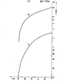
- an approximately 0.6 ⁇ m thick transparent film is produced on a silicon wafer with a silicon dioxide surface by spinning at approximately 4000 rpm.
- the resist 5 which is partially covered by a slit mask, is irradiated with a low-pressure mercury lamp for different lengths of time.
- the film is then at 20 ° C Developed in a developer mixture of methyl ethyl ketone and ethanol for 2 minutes, rinsed and then dried at approx. 120 ° C for 30 minutes.
- the affected areas are extracted to different extents by the developer, depending on the dose, so that a contrast curve is obtained directly.
- the actual thickness remaining in the non-irradiated area is approximately 97 to 100% of the original film thickness.
Landscapes
- Physics & Mathematics (AREA)
- General Physics & Mathematics (AREA)
- Engineering & Computer Science (AREA)
- Spectroscopy & Molecular Physics (AREA)
- Electromagnetism (AREA)
- Radar, Positioning & Navigation (AREA)
- Automation & Control Theory (AREA)
- Addition Polymer Or Copolymer, Post-Treatments, Or Chemical Modifications (AREA)
- Exposure And Positioning Against Photoresist Photosensitive Materials (AREA)
- Photosensitive Polymer And Photoresist Processing (AREA)
- Exposure Of Semiconductors, Excluding Electron Or Ion Beam Exposure (AREA)
- Materials For Photolithography (AREA)
Priority Applications (1)
| Application Number | Priority Date | Filing Date | Title |
|---|---|---|---|
| AT81107370T ATE21779T1 (de) | 1980-09-29 | 1981-09-17 | Verfahren zur herstellung von resiststrukturen. |
Applications Claiming Priority (2)
| Application Number | Priority Date | Filing Date | Title |
|---|---|---|---|
| DE19803036615 DE3036615A1 (de) | 1980-09-29 | 1980-09-29 | Verfahren zur herstellung von resiststrukturen |
| DE3036615 | 1980-09-29 |
Publications (3)
| Publication Number | Publication Date |
|---|---|
| EP0048899A2 true EP0048899A2 (fr) | 1982-04-07 |
| EP0048899A3 EP0048899A3 (en) | 1983-01-19 |
| EP0048899B1 EP0048899B1 (fr) | 1986-08-27 |
Family
ID=6113074
Family Applications (1)
| Application Number | Title | Priority Date | Filing Date |
|---|---|---|---|
| EP81107370A Expired EP0048899B1 (fr) | 1980-09-29 | 1981-09-17 | Procédé de formation de réserves |
Country Status (6)
| Country | Link |
|---|---|
| US (1) | US4395481A (fr) |
| EP (1) | EP0048899B1 (fr) |
| JP (1) | JPS57118240A (fr) |
| AT (1) | ATE21779T1 (fr) |
| CA (1) | CA1176902A (fr) |
| DE (2) | DE3036615A1 (fr) |
Cited By (5)
| Publication number | Priority date | Publication date | Assignee | Title |
|---|---|---|---|---|
| EP0076524A1 (fr) * | 1981-10-06 | 1983-04-13 | Kabushiki Kaisha Toshiba | Réserve de type positif sensible aux rayons |
| US4675270A (en) * | 1986-02-10 | 1987-06-23 | Loctite (Ireland) Limited | Imaging method for vapor deposited photoresists of anionically polymerizable monomer |
| US5187048A (en) * | 1989-06-23 | 1993-02-16 | Loctite (Ireland) Limited | Photoresists formed by polymerization of di-unsaturated monomers |
| US5359101A (en) * | 1989-11-21 | 1994-10-25 | Loctite Ireland, Ltd. | Anionically polymerizable monomers, polymers thereof and use of such polymers in photoresists |
| JP2016012104A (ja) * | 2014-06-30 | 2016-01-21 | 大日本印刷株式会社 | ポジ型レジスト組成物及びその製造方法、並びに、当該ポジ型レジスト組成物を用いたレジストパターンの製造方法 |
Families Citing this family (7)
| Publication number | Priority date | Publication date | Assignee | Title |
|---|---|---|---|---|
| US4536240A (en) | 1981-12-02 | 1985-08-20 | Advanced Semiconductor Products, Inc. | Method of forming thin optical membranes |
| DE3246825A1 (de) * | 1982-02-24 | 1983-09-01 | Max Planck Gesellschaft zur Förderung der Wissenschaften e.V., 3400 Göttingen | Positives resistmaterial |
| US4609615A (en) * | 1983-03-31 | 1986-09-02 | Oki Electric Industry Co., Ltd. | Process for forming pattern with negative resist using quinone diazide compound |
| US4675273A (en) * | 1986-02-10 | 1987-06-23 | Loctite (Ireland) Limited | Resists formed by vapor deposition of anionically polymerizable monomer |
| US6179922B1 (en) | 1998-07-10 | 2001-01-30 | Ball Semiconductor, Inc. | CVD photo resist deposition |
| US6686429B2 (en) * | 2001-05-11 | 2004-02-03 | Clariant Finance (Bvi) Limited | Polymer suitable for photoresist compositions |
| US7659050B2 (en) * | 2005-06-07 | 2010-02-09 | International Business Machines Corporation | High resolution silicon-containing resist |
Family Cites Families (9)
| Publication number | Priority date | Publication date | Assignee | Title |
|---|---|---|---|---|
| US4011351A (en) * | 1975-01-29 | 1977-03-08 | International Business Machines Corporation | Preparation of resist image with methacrylate polymers |
| CA1106600A (fr) * | 1977-07-25 | 1981-08-11 | Boris S. Dolzhenkov | Agitation au gaz en circulation des metaux en fusion |
| JPS5466122A (en) * | 1977-11-07 | 1979-05-28 | Fujitsu Ltd | Pattern formation material |
| JPS5484978A (en) * | 1977-12-20 | 1979-07-06 | Cho Lsi Gijutsu Kenkyu Kumiai | Method of forming pattern |
| AU4719279A (en) * | 1978-05-22 | 1979-11-29 | Western Electric Co. Inc. | Lithographic resist and device processing utilizing same |
| JPS5518638A (en) * | 1978-07-27 | 1980-02-08 | Chiyou Lsi Gijutsu Kenkyu Kumiai | Ionized radiation sensitive positive type resist |
| JPS55140836A (en) * | 1979-04-19 | 1980-11-04 | Fujitsu Ltd | Pattern forming method |
| JPS5653114A (en) * | 1979-10-08 | 1981-05-12 | Kohjin Co Ltd | Preparation of polymeric material for positive resist sensitive to radiation and far ultraviolet rays |
| JPS5654434A (en) * | 1979-10-11 | 1981-05-14 | Kohjin Co Ltd | Radiation and far ultraviolet ray sensitive positive type resist method |
-
1980
- 1980-09-29 DE DE19803036615 patent/DE3036615A1/de not_active Withdrawn
-
1981
- 1981-09-17 AT AT81107370T patent/ATE21779T1/de not_active IP Right Cessation
- 1981-09-17 DE DE8181107370T patent/DE3175216D1/de not_active Expired
- 1981-09-17 EP EP81107370A patent/EP0048899B1/fr not_active Expired
- 1981-09-24 JP JP56151340A patent/JPS57118240A/ja active Granted
- 1981-09-25 US US06/305,798 patent/US4395481A/en not_active Expired - Fee Related
- 1981-09-28 CA CA000386772A patent/CA1176902A/fr not_active Expired
Cited By (5)
| Publication number | Priority date | Publication date | Assignee | Title |
|---|---|---|---|---|
| EP0076524A1 (fr) * | 1981-10-06 | 1983-04-13 | Kabushiki Kaisha Toshiba | Réserve de type positif sensible aux rayons |
| US4675270A (en) * | 1986-02-10 | 1987-06-23 | Loctite (Ireland) Limited | Imaging method for vapor deposited photoresists of anionically polymerizable monomer |
| US5187048A (en) * | 1989-06-23 | 1993-02-16 | Loctite (Ireland) Limited | Photoresists formed by polymerization of di-unsaturated monomers |
| US5359101A (en) * | 1989-11-21 | 1994-10-25 | Loctite Ireland, Ltd. | Anionically polymerizable monomers, polymers thereof and use of such polymers in photoresists |
| JP2016012104A (ja) * | 2014-06-30 | 2016-01-21 | 大日本印刷株式会社 | ポジ型レジスト組成物及びその製造方法、並びに、当該ポジ型レジスト組成物を用いたレジストパターンの製造方法 |
Also Published As
| Publication number | Publication date |
|---|---|
| CA1176902A (fr) | 1984-10-30 |
| JPH0149935B2 (fr) | 1989-10-26 |
| JPS57118240A (en) | 1982-07-23 |
| DE3175216D1 (en) | 1986-10-02 |
| EP0048899B1 (fr) | 1986-08-27 |
| EP0048899A3 (en) | 1983-01-19 |
| ATE21779T1 (de) | 1986-09-15 |
| US4395481A (en) | 1983-07-26 |
| DE3036615A1 (de) | 1982-05-13 |
Similar Documents
| Publication | Publication Date | Title |
|---|---|---|
| EP0342498B1 (fr) | Composition photosensible positives ou négatives et procédé pour la fabrication d'images en relief | |
| EP0031592B1 (fr) | Composition photopolymérisable et matériau à copier photopolymérisable fabriqué à partir de cette composition | |
| DE69709874T2 (de) | Wässerige antireflexbeschichtung für photoresistzusammnesetzungen | |
| EP0184044B1 (fr) | Composition photosensible, matériel pour l'enregistrement préparé à partir de cette composition, et procédé pour la réalisation d'images en relief résistantes à la chaleur | |
| DE19956531A1 (de) | Vernetzer für ein Photoresist und diesen enthaltende Photoresistzusammensetzung | |
| DE3337024A1 (de) | Lichtempfindliche, trichlormethylgruppen aufweisende verbindungen, verfahren zu ihrer herstellung und diese verbindungen enthaltendes lichtempfindliches gemisch | |
| EP0164620A2 (fr) | Solution de revêtement photosensible positive | |
| EP0048899B1 (fr) | Procédé de formation de réserves | |
| EP0342495A2 (fr) | Composition photosensible et procédé pour la fabrication d'images en relief | |
| EP0143437A2 (fr) | Procédé pour fabriquer des patrons de réserve et film de réserve à sec pour ce procédé | |
| DE4008815A1 (de) | Photopolymerisierbares gemisch und daraus hergestelltes aufzeichnungsmaterial | |
| DE3134158A1 (de) | "zusammensetzung und verfahren zur ultrafeinen musterbildung" | |
| DE68929206T2 (de) | Lithographisches Verfahren zur Herstellung einer Vorrichtung | |
| DE2743763A1 (de) | Positivlackmaterial und verfahren zur herstellung einer lackmaske | |
| EP0176871A2 (fr) | Procédé pour la fabrication d'une photoréserve | |
| DE69129171T2 (de) | Verfahren zur dimensionellen Stabilisierung von Photopolymer-Flexodruckplatten | |
| DE4207264B4 (de) | Negativ arbeitendes strahlungsempfindliches Gemisch und damit hergestelltes Aufzeichnungsmaterial | |
| DE2645113C2 (de) | Mit Wasser entwickelbares, lichtempfindliches Gemisch für Drucksiebe, mit Wasser entwickelbares Drucksieb und Verfahren zu seiner Herstellung | |
| DE3208659A1 (de) | Bildreproduktionsmaterial und verfahren zu seiner herstellung | |
| EP0143380B1 (fr) | Composition photoréserve | |
| DE4126409A1 (de) | Strahlungsempfindliches gemisch mit einem polymeren bindemittel mit einheiten aus (alpha)-(beta)-ungesaettigten carbonsaeuren | |
| EP0226741B1 (fr) | Procédé pour la préparation d'une photoréserve positive | |
| EP0410256A1 (fr) | Composition photosensible | |
| EP0140353A2 (fr) | Matériel d'enregistrement photopolymérisable pour la fabrication de plaques d'impression et procédé pour la fabrication de plaques d'impression avec ce matériel | |
| DE3036710C2 (fr) |
Legal Events
| Date | Code | Title | Description |
|---|---|---|---|
| PUAI | Public reference made under article 153(3) epc to a published international application that has entered the european phase |
Free format text: ORIGINAL CODE: 0009012 |
|
| 17P | Request for examination filed |
Effective date: 19811028 |
|
| AK | Designated contracting states |
Designated state(s): AT BE CH DE FR GB IT NL SE |
|
| PUAL | Search report despatched |
Free format text: ORIGINAL CODE: 0009013 |
|
| AK | Designated contracting states |
Designated state(s): AT BE CH DE FR GB IT LI NL SE |
|
| GRAA | (expected) grant |
Free format text: ORIGINAL CODE: 0009210 |
|
| AK | Designated contracting states |
Kind code of ref document: B1 Designated state(s): AT BE CH DE FR GB IT LI NL SE |
|
| REF | Corresponds to: |
Ref document number: 21779 Country of ref document: AT Date of ref document: 19860915 Kind code of ref document: T |
|
| REF | Corresponds to: |
Ref document number: 3175216 Country of ref document: DE Date of ref document: 19861002 |
|
| ET | Fr: translation filed | ||
| ITF | It: translation for a ep patent filed | ||
| PLBE | No opposition filed within time limit |
Free format text: ORIGINAL CODE: 0009261 |
|
| STAA | Information on the status of an ep patent application or granted ep patent |
Free format text: STATUS: NO OPPOSITION FILED WITHIN TIME LIMIT |
|
| 26N | No opposition filed | ||
| PGFP | Annual fee paid to national office [announced via postgrant information from national office to epo] |
Ref country code: AT Payment date: 19890825 Year of fee payment: 9 |
|
| PGFP | Annual fee paid to national office [announced via postgrant information from national office to epo] |
Ref country code: GB Payment date: 19890831 Year of fee payment: 9 |
|
| PGFP | Annual fee paid to national office [announced via postgrant information from national office to epo] |
Ref country code: SE Payment date: 19890912 Year of fee payment: 9 |
|
| PGFP | Annual fee paid to national office [announced via postgrant information from national office to epo] |
Ref country code: BE Payment date: 19890919 Year of fee payment: 9 |
|
| PGFP | Annual fee paid to national office [announced via postgrant information from national office to epo] |
Ref country code: FR Payment date: 19890928 Year of fee payment: 9 |
|
| ITTA | It: last paid annual fee | ||
| PGFP | Annual fee paid to national office [announced via postgrant information from national office to epo] |
Ref country code: NL Payment date: 19890930 Year of fee payment: 9 |
|
| PGFP | Annual fee paid to national office [announced via postgrant information from national office to epo] |
Ref country code: DE Payment date: 19891127 Year of fee payment: 9 |
|
| PGFP | Annual fee paid to national office [announced via postgrant information from national office to epo] |
Ref country code: CH Payment date: 19891218 Year of fee payment: 9 |
|
| PG25 | Lapsed in a contracting state [announced via postgrant information from national office to epo] |
Ref country code: GB Effective date: 19900917 Ref country code: AT Effective date: 19900917 |
|
| PG25 | Lapsed in a contracting state [announced via postgrant information from national office to epo] |
Ref country code: SE Effective date: 19900918 |
|
| PG25 | Lapsed in a contracting state [announced via postgrant information from national office to epo] |
Ref country code: LI Effective date: 19900930 Ref country code: CH Effective date: 19900930 Ref country code: BE Effective date: 19900930 |
|
| BERE | Be: lapsed |
Owner name: SIEMENS A.G. BERLIN UND MUNCHEN Effective date: 19900930 |
|
| PG25 | Lapsed in a contracting state [announced via postgrant information from national office to epo] |
Ref country code: NL Effective date: 19910401 |
|
| GBPC | Gb: european patent ceased through non-payment of renewal fee | ||
| NLV4 | Nl: lapsed or anulled due to non-payment of the annual fee | ||
| PG25 | Lapsed in a contracting state [announced via postgrant information from national office to epo] |
Ref country code: FR Effective date: 19910530 |
|
| REG | Reference to a national code |
Ref country code: CH Ref legal event code: PL |
|
| PG25 | Lapsed in a contracting state [announced via postgrant information from national office to epo] |
Ref country code: DE Effective date: 19910601 |
|
| REG | Reference to a national code |
Ref country code: FR Ref legal event code: ST |
|
| EUG | Se: european patent has lapsed |
Ref document number: 81107370.9 Effective date: 19910527 |