EP0049388A2 - Détecteur de signal vidéo - Google Patents
Détecteur de signal vidéo Download PDFInfo
- Publication number
- EP0049388A2 EP0049388A2 EP81107298A EP81107298A EP0049388A2 EP 0049388 A2 EP0049388 A2 EP 0049388A2 EP 81107298 A EP81107298 A EP 81107298A EP 81107298 A EP81107298 A EP 81107298A EP 0049388 A2 EP0049388 A2 EP 0049388A2
- Authority
- EP
- European Patent Office
- Prior art keywords
- video signal
- signal
- input
- output
- peak detector
- Prior art date
- Legal status (The legal status is an assumption and is not a legal conclusion. Google has not performed a legal analysis and makes no representation as to the accuracy of the status listed.)
- Granted
Links
Images


Classifications
-
- G—PHYSICS
- G06—COMPUTING OR CALCULATING; COUNTING
- G06V—IMAGE OR VIDEO RECOGNITION OR UNDERSTANDING
- G06V30/00—Character recognition; Recognising digital ink; Document-oriented image-based pattern recognition
- G06V30/10—Character recognition
- G06V30/16—Image preprocessing
- G06V30/162—Quantising the image signal
-
- G—PHYSICS
- G06—COMPUTING OR CALCULATING; COUNTING
- G06V—IMAGE OR VIDEO RECOGNITION OR UNDERSTANDING
- G06V30/00—Character recognition; Recognising digital ink; Document-oriented image-based pattern recognition
- G06V30/10—Character recognition
Definitions
- the present invention relates to a video signal detector and more specifically to a device for converting an analog video input signal into the digital output signal.
- the optical detector is usually a photo multiplier tube or a string of light diodes that detect the reflected light from a passing illuminated document.
- the detected signals are amplified and gated into a threshold circuit functioning as a video signal detector, whereupon the detected digital video signals are gated through a memory to a character recognition device. In this way it is possible to read and recognize the text of a document to be forwarded to a user unit.
- a video signal detector in such a system for optical document reading is shown in the US patent 3912943.
- a signal threshold circuit is used to distinguish an input analog high white signal level from an input low black signal level, the output of the circuit delivering a digital "one" signal for the high white level and a "zero" signal for the low black level.
- a threshold signal is used to detect white one signals. This threshold signal is adjusted dynamically through a white peak signal and a black peak signal as well as through a jump circuit that considers the momentaneous fall of the white peak signal. Through this dynamic change of the threshold level the device is able to detect video signal curves of different quality without erroneous detection caused by direct noise.
- the advantage of the present invention as compared to the prior art is the realization of a low cost optical signal detection system with increased signal detection capacity.
- the terminal 1 is a video signal input for an amplified video signal that for instance is achieved from a photomultiplier tube or from the output of a number of detecting light diodes.
- the imput 1 is connected through a resistor R3 to a first input of an input amplifier 5 as well as to one terminal of a condenser C3.
- the output from the amplifier 5 that is connected to the second terminal of the condenser C3 is also connected through a diode D3 and a condenser Cl to ground.
- the second input of the amplifier 5 is connected through a resistor R9 to ground.
- the common node 12 of the diode D3 and the condenser Cl is connected to the first input of the second amplifier 3.
- the second input of the amplifier 3 is connected to a common node of two resistors R6 and R7, where the second terminal of R7 is grounded.
- a resistor R5 is connected through both inputs of the amplifier 3.
- the output from the amplifier 3 is connected to the second terminal of the resistor R6 and through a resistor R8 to the common node of a number of resistors R10.
- This common node is connected through a resistor R4 to the threshold signal input 17 of an output amplifier 6.
- the resistors R10 are connected to a threshold signal level adjusting circuit 7.
- the output from the amplifier 5 is further connected through a test and hold circuit 19 and an amplifier circuit 8 to the first input 18 of the output amplifier 6.
- the output 15 from the test and hold circuit 19 is also connected through a backbiased diode Dl and a condenser C2 to ground.
- the common node 14 of diode Dl and condenser C2 is connected through a resistor Rl to the first input 18 of the output amplifier 6 as well as to a first input of a third amplifier 4.
- the output of the amplifier 4 is fed back to its second input and is further connected through a diode D2 to the adjustment point of a resistor R2.
- One terminal of the resistor R2 is connected to ground and the second terminal is connected to the common node 16 of resistors R4 and R10.
- the output from the output amplifier 6 is connected to an output terminal 2, is further fed back through a resistor R 12 to its second input 17 and is connected through a resistor R13 to a potential terminal 9.
- a switch 10 is connected through the two terminals of condenser C3 in order to selectively short circuit the condenser C3.
- the video signal detector circuit according to fig. 1 comprises an inverting integrator in the form of the amplifier 5, the condenser C3 and the resistor R9.
- the diode D3 and the condenser Cl form together a white peak detector, and the diode Dl and the condenser C2 form a black peak detector.
- the adjustable resistor R2 forms an adjustable device defining the share of the white signal peak and black signal peak when setting the threshold signal level at the second input terminal 17 of the output amplifier 6.
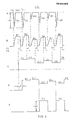
- Fig. 2 shows the curve 20 which is the delayed video signal that appears at the input terminal 18 of the output amplifier 6. This signal corresponds to the input signal at the terminal 1 and differs from said input signal because the amplifier 5 has integrated the input signal, and the test hold circuit 19 as well as the delay circuit 8 have delayed the signal a certain time.
- the curve 30 of fig. 2 corresponds to the threshold level signal curve that appears at the second input terminal 17 of the output amplifier 6.
- the curve 40 of fig. 2 shows the detected data signal curve that appears at the output terminal 2.
- the arriving video signal after integration changes from a low value to a high value that corresponds to the detection of a white area on the document.
- This high signal value is represented by the curve portion 21 on the video signal curve 20.
- the condenser Cl of the white peak detector is then charged, and the voltage level at the terminal 12 will slowly rise to maximum value at point 26.
- the signal level at the terminal 17 will rise as well as is shown by the first portion of curve 30.
- the signal level at the terminal 18 is higher than the signal level at the terminal 17 as is shown in fig. 2 by the distance "a" between the curve portion 21 and the beginning of the curve 30.
- This threshold level difference is set by means of the adjustable circuit 7 through selectively activating the adjustable resistors 10.
- the threshold curve 30 should have the same slope as the video signal curve portion 21 in order for a constant threshold value "a" to be maintained. This slope is a result of the characteristics of the optical components and their location in the detector device, the threshold compensation being controlled or programmed in the circuit 7.
- the input video signal curve will fall from the high value 21 to a low portion 22 according to fig. 2.
- the condenser C2 of the black peak detector will then be discharged to a signal level that corresponds to the black peak of the curve portion 22. Since the signal level 22 is sufficiently low, the diode D2 will not be biased any more, and the signal level at the terminal 17 falls as shown by the curve portion 31. It is seen that the threshold signal level at point 17 falls earlier than the video signal level at the terminal 18 which is due to the influence of the delay circuit 8. As the threshold level now is higher than the video signal level at the input of the output amplifier 6, an output signal will appear on the output terminal 2 as shown by the curve portion 41 of the output signal 40, fig. 2.
- the input video signal rises to a value represented by the curve portion 23 which is considerably lower than the normal white video signal input represented by the signal level 21. Thanks to the influence of the black peak detector the threshold signal at the terminal 17 will still have a low value, and the output signal at the terminal 2 will fall to its low value. After that, the video signal will fall again to a low value as represented by the curve portion 24. The threshold signal at the terminal 17 will once again be higher than the video signal input at the terminal 18, and the result is another output signal at the terminal 2. This is shown by the curve portion 42 of the output signal 40.
- Fig. 3 shows the same signal curves as fig. 2 but the contrast is low between the background and the character information on the detected document.
- the video signal curve 50 appears, to begin with, as a white signal portion 51 corresponding to the signal curve portion 21 of fig. 2.
- the threshold signal curve 60 corresponds to the threshold signal curve 30 of the fig. 2.
- this signal level fall is much less pronounced due to the low contrast as compared to the corresponding signal level fall from curve portion 21 to curve portion 22 of fig. 2. If the threshold signal 60 had showed the same fall as in fig. 2, the detection of the black peak of the curve portion 52 would be uncertain. From fig.
- the black peak detector will not be activated at comparatively high signal levels due to the fact that the diode D2 is biased.
- the threshold level at the terminal 17 will thus not be influenced by the black peak detector but only by the white peak detector. So no jumps will occur in the threshold level signal curve 60 of fig. 3.
- the feedback resistor R12 is used to lock the output signal on terminal 2 in order to avoid output signal oscillations when the signal levels of the input terminals 17 and 18 cross eachother.
- the video signal detector according to fig. 1 is able to detect high as well as low contrast signals. It should be noted that if a high contrast signal suddenly appears in between a number of low contrast signals according to fig. 3, the black peak detector of fig. 1 will immediately be activated and a correct signal detection will be achieved. Even single low contrast signals that are mixed with high contrast signals 22, 24 according to fig. 2 can most often be detected successfully. This is due to the fact that the condenser C2 is charged through the resistor Rl to a value high enough for the diode D2 to be able to stop the influence of the black peak detector on the threshold level 33. The pulse 43 shows the detected data pulse.
- the circuit according to fig. 1 is able to consider all possibilities of black/white contrast for the input video signal.
- a dynamic threshold level curve is achieved that provides a maximum detection of video signals at the same time as noise signals are eliminated.
- the signal level indicated by the curves A-F of fig. 4 are used in the detector circuit according to fig. 1.
- the curve A illustrates the input video signal at the terminal 1, the individual pulses Al-A6 having a maximum am- plitud of -7V and a pulse interval of 5 p s.
- the curve B disclosing the individual signals B1-B6 illustrates the integrated video signal at the terminal 11, and the curve C having the individual signals Cl-C6 shows the video signal after the test and hold circuit 19 at the terminal 15.
- the curve E having the signals El-E6 indicates the signal level at the terminal 18 and corresponds substantially to the curve C except for the delay K that is caused by the delay circuit 8.
- the output signal F at the terminal 2 is represented by two pulses F3 and F5 of amplitude +5V for TTL- logic.
- test and hold circuit 19 should be activated by a first control signal Tl before the switch 10 is activated by a second control signal T2, which is shown in fig. 4.
Landscapes
- Engineering & Computer Science (AREA)
- Computer Vision & Pattern Recognition (AREA)
- Physics & Mathematics (AREA)
- General Physics & Mathematics (AREA)
- Multimedia (AREA)
- Theoretical Computer Science (AREA)
- Image Input (AREA)
- Facsimile Image Signal Circuits (AREA)
- Manipulation Of Pulses (AREA)
- Facsimile Scanning Arrangements (AREA)
Applications Claiming Priority (2)
| Application Number | Priority Date | Filing Date | Title |
|---|---|---|---|
| SE8007037A SE448921B (sv) | 1980-10-08 | 1980-10-08 | Videosignaldetektor for detektering av inkommande analoga videosignaler fran en optisk dokumentlesare och for avgivande av digitala utgangssignaler |
| SE8007037 | 1980-10-08 |
Publications (3)
| Publication Number | Publication Date |
|---|---|
| EP0049388A2 true EP0049388A2 (fr) | 1982-04-14 |
| EP0049388A3 EP0049388A3 (en) | 1984-08-22 |
| EP0049388B1 EP0049388B1 (fr) | 1987-01-14 |
Family
ID=20341932
Family Applications (1)
| Application Number | Title | Priority Date | Filing Date |
|---|---|---|---|
| EP81107298A Expired EP0049388B1 (fr) | 1980-10-08 | 1981-09-16 | Détecteur de signal vidéo |
Country Status (5)
| Country | Link |
|---|---|
| US (1) | US4447774A (fr) |
| EP (1) | EP0049388B1 (fr) |
| JP (1) | JPS5784679A (fr) |
| DE (1) | DE3175836D1 (fr) |
| SE (1) | SE448921B (fr) |
Cited By (2)
| Publication number | Priority date | Publication date | Assignee | Title |
|---|---|---|---|---|
| US4584703A (en) * | 1981-12-23 | 1986-04-22 | International Business Machines Corporation | Character recognition system and its use in an optical document reader |
| AU603655B2 (en) * | 1987-04-22 | 1990-11-22 | Abbott Laboratories | Printed optical code reader and format |
Families Citing this family (3)
| Publication number | Priority date | Publication date | Assignee | Title |
|---|---|---|---|---|
| JPS5873280A (ja) * | 1981-10-27 | 1983-05-02 | Hitachi Ltd | 信号2値化処理装置 |
| US6191626B1 (en) * | 1998-08-17 | 2001-02-20 | Texas Instruments Incorporated | Method and apparatus for compensating input threshold variations on input buffers |
| US7330164B2 (en) * | 2003-08-25 | 2008-02-12 | Thomson Licensing | Video controlled detector sensitivity |
Family Cites Families (8)
| Publication number | Priority date | Publication date | Assignee | Title |
|---|---|---|---|---|
| US3566281A (en) * | 1968-05-21 | 1971-02-23 | Ibm | Electric pulse wave clipping circuitry |
| US3599148A (en) * | 1969-04-22 | 1971-08-10 | Burroughs Corp | Quantizing circuit correction for character recognition systems |
| US3599151A (en) * | 1969-12-29 | 1971-08-10 | Ibm | Character recognition photosensing apparatus having a threshold comparator circuit |
| US3912943A (en) * | 1974-08-09 | 1975-10-14 | Ibm | Video thresholder |
| JPS5356918A (en) * | 1976-11-01 | 1978-05-23 | Oki Electric Ind Co Ltd | Picture read system |
| US4121121A (en) * | 1977-09-13 | 1978-10-17 | Computer Identics Corporation | Follower response control circuit |
| JPS5579567A (en) * | 1978-12-12 | 1980-06-16 | Ricoh Co Ltd | Shading correction system |
| US4227218A (en) * | 1978-12-14 | 1980-10-07 | Exxon Research & Engineering Co. | Method and apparatus for generating a digital facsimile signal |
-
1980
- 1980-10-08 SE SE8007037A patent/SE448921B/sv not_active IP Right Cessation
-
1981
- 1981-09-14 JP JP56144079A patent/JPS5784679A/ja active Granted
- 1981-09-16 EP EP81107298A patent/EP0049388B1/fr not_active Expired
- 1981-09-16 DE DE8181107298T patent/DE3175836D1/de not_active Expired
- 1981-09-28 US US06/306,632 patent/US4447774A/en not_active Expired - Lifetime
Cited By (2)
| Publication number | Priority date | Publication date | Assignee | Title |
|---|---|---|---|---|
| US4584703A (en) * | 1981-12-23 | 1986-04-22 | International Business Machines Corporation | Character recognition system and its use in an optical document reader |
| AU603655B2 (en) * | 1987-04-22 | 1990-11-22 | Abbott Laboratories | Printed optical code reader and format |
Also Published As
| Publication number | Publication date |
|---|---|
| JPS5784679A (en) | 1982-05-27 |
| EP0049388A3 (en) | 1984-08-22 |
| DE3175836D1 (en) | 1987-02-19 |
| JPS6156672B2 (fr) | 1986-12-03 |
| US4447774A (en) | 1984-05-08 |
| EP0049388B1 (fr) | 1987-01-14 |
| SE448921B (sv) | 1987-03-23 |
| SE8007037L (sv) | 1982-04-09 |
Similar Documents
| Publication | Publication Date | Title |
|---|---|---|
| US4163909A (en) | Peak detecting circuitry and dual threshold circuitry therefor | |
| NL8005789A (nl) | Informatie-extractieschakeling. | |
| US4801788A (en) | Bar code scanner for a video signal which has a shading waveform | |
| US3692983A (en) | Automatic threshold control circuit for optical card readers and sorters | |
| KR930006799B1 (ko) | 바 코드 판독시스템 및 그 장치 | |
| US3541457A (en) | Peak occurrence detector circuit | |
| JP2571683B2 (ja) | 符号読取装置の信号増幅回路 | |
| EP0049388B1 (fr) | Détecteur de signal vidéo | |
| SE452936B (sv) | Kretsanordning for omvandling av en fran en uppteckningsberare avlest informationssignal till en fyrkantsignal | |
| US3461300A (en) | Automatic gain control circuit for optical sensor | |
| JPS58154957A (ja) | デジタルデ−タ検知回路 | |
| US3368153A (en) | Shaper for producing uniform rectangular pulses from variously shaped signals | |
| US5864129A (en) | Bar code digitizer including a voltage comparator | |
| EP0505970B1 (fr) | Circuit pour détecter le niveau du blanc pour un balayeur optique | |
| US4485319A (en) | Bubble memory sense amplifier | |
| US5965864A (en) | Slicing ratio controlling circuit | |
| JP2856787B2 (ja) | 2値化回路、中間レベル検出回路及びピーク包絡線検出回路 | |
| US4078227A (en) | Threshold detector for optical character recognition system | |
| JPS6129078Y2 (fr) | ||
| JPS6151662A (ja) | 信号検出回路 | |
| US5350950A (en) | Setting circuit of binary threshold value | |
| JPS589470B2 (ja) | 二値信号発生回路 | |
| JP2572805B2 (ja) | マーク読取り機のマーク判別回路 | |
| JPH021946Y2 (fr) | ||
| JP2756468B2 (ja) | 二値化回路 |
Legal Events
| Date | Code | Title | Description |
|---|---|---|---|
| PUAI | Public reference made under article 153(3) epc to a published international application that has entered the european phase |
Free format text: ORIGINAL CODE: 0009012 |
|
| 17P | Request for examination filed |
Effective date: 19810916 |
|
| AK | Designated contracting states |
Designated state(s): DE FR GB |
|
| PUAL | Search report despatched |
Free format text: ORIGINAL CODE: 0009013 |
|
| AK | Designated contracting states |
Designated state(s): DE FR GB |
|
| GRAA | (expected) grant |
Free format text: ORIGINAL CODE: 0009210 |
|
| AK | Designated contracting states |
Kind code of ref document: B1 Designated state(s): DE FR GB |
|
| REF | Corresponds to: |
Ref document number: 3175836 Country of ref document: DE Date of ref document: 19870219 |
|
| ET | Fr: translation filed | ||
| PLBE | No opposition filed within time limit |
Free format text: ORIGINAL CODE: 0009261 |
|
| STAA | Information on the status of an ep patent application or granted ep patent |
Free format text: STATUS: NO OPPOSITION FILED WITHIN TIME LIMIT |
|
| 26N | No opposition filed | ||
| PGFP | Annual fee paid to national office [announced via postgrant information from national office to epo] |
Ref country code: GB Payment date: 19910823 Year of fee payment: 11 |
|
| PGFP | Annual fee paid to national office [announced via postgrant information from national office to epo] |
Ref country code: FR Payment date: 19910903 Year of fee payment: 11 |
|
| PGFP | Annual fee paid to national office [announced via postgrant information from national office to epo] |
Ref country code: DE Payment date: 19910926 Year of fee payment: 11 |
|
| PG25 | Lapsed in a contracting state [announced via postgrant information from national office to epo] |
Ref country code: GB Effective date: 19920916 |
|
| GBPC | Gb: european patent ceased through non-payment of renewal fee |
Effective date: 19920916 |
|
| PG25 | Lapsed in a contracting state [announced via postgrant information from national office to epo] |
Ref country code: FR Effective date: 19930528 |
|
| PG25 | Lapsed in a contracting state [announced via postgrant information from national office to epo] |
Ref country code: DE Effective date: 19930602 |
|
| REG | Reference to a national code |
Ref country code: FR Ref legal event code: ST |