EP0049799A2 - Photomask blank and photomask - Google Patents
Photomask blank and photomask Download PDFInfo
- Publication number
- EP0049799A2 EP0049799A2 EP81107702A EP81107702A EP0049799A2 EP 0049799 A2 EP0049799 A2 EP 0049799A2 EP 81107702 A EP81107702 A EP 81107702A EP 81107702 A EP81107702 A EP 81107702A EP 0049799 A2 EP0049799 A2 EP 0049799A2
- Authority
- EP
- European Patent Office
- Prior art keywords
- film
- oxide
- photomask
- metallic
- chromium
- Prior art date
- Legal status (The legal status is an assumption and is not a legal conclusion. Google has not performed a legal analysis and makes no representation as to the accuracy of the status listed.)
- Granted
Links
- 230000000873 masking effect Effects 0.000 claims abstract description 41
- 239000011651 chromium Substances 0.000 claims abstract description 31
- 229910052804 chromium Inorganic materials 0.000 claims abstract description 26
- 239000000463 material Substances 0.000 claims abstract description 25
- 239000000758 substrate Substances 0.000 claims abstract description 24
- 229910052710 silicon Inorganic materials 0.000 claims abstract description 22
- 239000010703 silicon Substances 0.000 claims abstract description 22
- VYZAMTAEIAYCRO-UHFFFAOYSA-N Chromium Chemical compound [Cr] VYZAMTAEIAYCRO-UHFFFAOYSA-N 0.000 claims abstract description 20
- 229910052715 tantalum Inorganic materials 0.000 claims abstract description 16
- VYPSYNLAJGMNEJ-UHFFFAOYSA-N Silicium dioxide Chemical compound O=[Si]=O VYPSYNLAJGMNEJ-UHFFFAOYSA-N 0.000 claims abstract description 15
- WGLPBDUCMAPZCE-UHFFFAOYSA-N Trioxochromium Chemical compound O=[Cr](=O)=O WGLPBDUCMAPZCE-UHFFFAOYSA-N 0.000 claims abstract description 14
- 229910000423 chromium oxide Inorganic materials 0.000 claims abstract description 14
- 229910052814 silicon oxide Inorganic materials 0.000 claims abstract description 13
- 230000001681 protective effect Effects 0.000 claims abstract description 10
- 229910052737 gold Inorganic materials 0.000 claims abstract description 5
- 229910052750 molybdenum Inorganic materials 0.000 claims abstract description 5
- 229910052758 niobium Inorganic materials 0.000 claims abstract description 5
- 229910052719 titanium Inorganic materials 0.000 claims abstract description 5
- 229910052721 tungsten Inorganic materials 0.000 claims abstract description 5
- 229910052720 vanadium Inorganic materials 0.000 claims abstract description 5
- 229910052726 zirconium Inorganic materials 0.000 claims abstract description 5
- SJKRCWUQJZIWQB-UHFFFAOYSA-N azane;chromium Chemical compound N.[Cr] SJKRCWUQJZIWQB-UHFFFAOYSA-N 0.000 claims abstract description 4
- 238000005530 etching Methods 0.000 claims description 25
- UQSXHKLRYXJYBZ-UHFFFAOYSA-N Iron oxide Chemical compound [Fe]=O UQSXHKLRYXJYBZ-UHFFFAOYSA-N 0.000 claims description 11
- GUVRBAGPIYLISA-UHFFFAOYSA-N tantalum atom Chemical compound [Ta] GUVRBAGPIYLISA-UHFFFAOYSA-N 0.000 claims description 10
- BPUBBGLMJRNUCC-UHFFFAOYSA-N oxygen(2-);tantalum(5+) Chemical compound [O-2].[O-2].[O-2].[O-2].[O-2].[Ta+5].[Ta+5] BPUBBGLMJRNUCC-UHFFFAOYSA-N 0.000 claims description 9
- 229910001936 tantalum oxide Inorganic materials 0.000 claims description 9
- 238000002834 transmittance Methods 0.000 claims description 7
- -1 chromium nitrides Chemical class 0.000 claims description 4
- 239000010936 titanium Substances 0.000 claims description 4
- GWEVSGVZZGPLCZ-UHFFFAOYSA-N Titan oxide Chemical compound O=[Ti]=O GWEVSGVZZGPLCZ-UHFFFAOYSA-N 0.000 claims description 3
- BRPQOXSCLDDYGP-UHFFFAOYSA-N calcium oxide Chemical compound [O-2].[Ca+2] BRPQOXSCLDDYGP-UHFFFAOYSA-N 0.000 claims description 3
- 239000000292 calcium oxide Substances 0.000 claims description 3
- ODINCKMPIJJUCX-UHFFFAOYSA-N calcium oxide Inorganic materials [Ca]=O ODINCKMPIJJUCX-UHFFFAOYSA-N 0.000 claims description 3
- 229910000420 cerium oxide Inorganic materials 0.000 claims description 3
- 239000000395 magnesium oxide Substances 0.000 claims description 3
- CPLXHLVBOLITMK-UHFFFAOYSA-N magnesium oxide Inorganic materials [Mg]=O CPLXHLVBOLITMK-UHFFFAOYSA-N 0.000 claims description 3
- AXZKOIWUVFPNLO-UHFFFAOYSA-N magnesium;oxygen(2-) Chemical compound [O-2].[Mg+2] AXZKOIWUVFPNLO-UHFFFAOYSA-N 0.000 claims description 3
- TWNQGVIAIRXVLR-UHFFFAOYSA-N oxo(oxoalumanyloxy)alumane Chemical compound O=[Al]O[Al]=O TWNQGVIAIRXVLR-UHFFFAOYSA-N 0.000 claims description 3
- BMMGVYCKOGBVEV-UHFFFAOYSA-N oxo(oxoceriooxy)cerium Chemical compound [Ce]=O.O=[Ce]=O BMMGVYCKOGBVEV-UHFFFAOYSA-N 0.000 claims description 3
- MZLGASXMSKOWSE-UHFFFAOYSA-N tantalum nitride Chemical compound [Ta]#N MZLGASXMSKOWSE-UHFFFAOYSA-N 0.000 claims description 3
- OGIDPMRJRNCKJF-UHFFFAOYSA-N titanium oxide Inorganic materials [Ti]=O OGIDPMRJRNCKJF-UHFFFAOYSA-N 0.000 claims description 3
- 229910052581 Si3N4 Inorganic materials 0.000 claims 2
- 235000013980 iron oxide Nutrition 0.000 claims 2
- HQVNEWCFYHHQES-UHFFFAOYSA-N silicon nitride Chemical compound N12[Si]34N5[Si]62N3[Si]51N64 HQVNEWCFYHHQES-UHFFFAOYSA-N 0.000 claims 2
- UOUJSJZBMCDAEU-UHFFFAOYSA-N chromium(3+);oxygen(2-) Chemical class [O-2].[O-2].[O-2].[Cr+3].[Cr+3] UOUJSJZBMCDAEU-UHFFFAOYSA-N 0.000 claims 1
- VBMVTYDPPZVILR-UHFFFAOYSA-N iron(2+);oxygen(2-) Chemical class [O-2].[Fe+2] VBMVTYDPPZVILR-UHFFFAOYSA-N 0.000 claims 1
- LIVNPJMFVYWSIS-UHFFFAOYSA-N silicon monoxide Chemical class [Si-]#[O+] LIVNPJMFVYWSIS-UHFFFAOYSA-N 0.000 claims 1
- 239000010408 film Substances 0.000 abstract description 104
- 239000012789 electroconductive film Substances 0.000 abstract description 24
- 238000010894 electron beam technology Methods 0.000 abstract description 18
- 239000000203 mixture Substances 0.000 abstract description 12
- 238000007689 inspection Methods 0.000 abstract description 6
- 238000005406 washing Methods 0.000 abstract description 5
- 230000006378 damage Effects 0.000 abstract description 4
- 238000000206 photolithography Methods 0.000 abstract description 2
- XUIMIQQOPSSXEZ-UHFFFAOYSA-N Silicon Chemical compound [Si] XUIMIQQOPSSXEZ-UHFFFAOYSA-N 0.000 description 19
- 238000000034 method Methods 0.000 description 16
- 239000000126 substance Substances 0.000 description 12
- 238000012360 testing method Methods 0.000 description 12
- 230000007547 defect Effects 0.000 description 9
- 239000011521 glass Substances 0.000 description 9
- 238000001312 dry etching Methods 0.000 description 7
- 239000004065 semiconductor Substances 0.000 description 7
- 235000012431 wafers Nutrition 0.000 description 7
- 238000012546 transfer Methods 0.000 description 6
- 238000001771 vacuum deposition Methods 0.000 description 6
- 239000000243 solution Substances 0.000 description 5
- BQCADISMDOOEFD-UHFFFAOYSA-N Silver Chemical compound [Ag] BQCADISMDOOEFD-UHFFFAOYSA-N 0.000 description 4
- 239000002253 acid Substances 0.000 description 4
- 239000000839 emulsion Substances 0.000 description 4
- 229920002120 photoresistant polymer Polymers 0.000 description 4
- 229910052709 silver Inorganic materials 0.000 description 4
- 239000004332 silver Substances 0.000 description 4
- 238000004544 sputter deposition Methods 0.000 description 4
- 238000010276 construction Methods 0.000 description 3
- 239000000428 dust Substances 0.000 description 3
- 239000007788 liquid Substances 0.000 description 3
- 238000004519 manufacturing process Methods 0.000 description 3
- 238000012216 screening Methods 0.000 description 3
- 238000010186 staining Methods 0.000 description 3
- 238000007738 vacuum evaporation Methods 0.000 description 3
- 238000001039 wet etching Methods 0.000 description 3
- QAOWNCQODCNURD-UHFFFAOYSA-N Sulfuric acid Chemical compound OS(O)(=O)=O QAOWNCQODCNURD-UHFFFAOYSA-N 0.000 description 2
- 150000007513 acids Chemical class 0.000 description 2
- 239000003513 alkali Substances 0.000 description 2
- 239000012298 atmosphere Substances 0.000 description 2
- 239000012459 cleaning agent Substances 0.000 description 2
- 230000007797 corrosion Effects 0.000 description 2
- 238000005260 corrosion Methods 0.000 description 2
- 238000000151 deposition Methods 0.000 description 2
- 238000011161 development Methods 0.000 description 2
- 230000005611 electricity Effects 0.000 description 2
- 238000007772 electroless plating Methods 0.000 description 2
- 238000011156 evaluation Methods 0.000 description 2
- 238000010438 heat treatment Methods 0.000 description 2
- 235000019988 mead Nutrition 0.000 description 2
- 238000005259 measurement Methods 0.000 description 2
- 229910052751 metal Inorganic materials 0.000 description 2
- 239000002184 metal Substances 0.000 description 2
- 239000003960 organic solvent Substances 0.000 description 2
- 239000005361 soda-lime glass Substances 0.000 description 2
- 239000010409 thin film Substances 0.000 description 2
- 229910000667 (NH4)2Ce(NO3)6 Inorganic materials 0.000 description 1
- MHAJPDPJQMAIIY-UHFFFAOYSA-N Hydrogen peroxide Chemical compound OO MHAJPDPJQMAIIY-UHFFFAOYSA-N 0.000 description 1
- ISWSIDIOOBJBQZ-UHFFFAOYSA-N Phenol Chemical compound OC1=CC=CC=C1 ISWSIDIOOBJBQZ-UHFFFAOYSA-N 0.000 description 1
- 238000009825 accumulation Methods 0.000 description 1
- 239000007864 aqueous solution Substances 0.000 description 1
- 230000004888 barrier function Effects 0.000 description 1
- SRSXLGNVWSONIS-UHFFFAOYSA-N benzenesulfonic acid Chemical compound OS(=O)(=O)C1=CC=CC=C1 SRSXLGNVWSONIS-UHFFFAOYSA-N 0.000 description 1
- 229940092714 benzenesulfonic acid Drugs 0.000 description 1
- 230000015572 biosynthetic process Effects 0.000 description 1
- 239000003795 chemical substances by application Substances 0.000 description 1
- KRVSOGSZCMJSLX-UHFFFAOYSA-L chromic acid Substances O[Cr](O)(=O)=O KRVSOGSZCMJSLX-UHFFFAOYSA-L 0.000 description 1
- 238000004140 cleaning Methods 0.000 description 1
- 238000000576 coating method Methods 0.000 description 1
- 230000006735 deficit Effects 0.000 description 1
- 230000002939 deleterious effect Effects 0.000 description 1
- 230000000694 effects Effects 0.000 description 1
- 230000003628 erosive effect Effects 0.000 description 1
- AWJWCTOOIBYHON-UHFFFAOYSA-N furo[3,4-b]pyrazine-5,7-dione Chemical compound C1=CN=C2C(=O)OC(=O)C2=N1 AWJWCTOOIBYHON-UHFFFAOYSA-N 0.000 description 1
- 239000007789 gas Substances 0.000 description 1
- 229910003437 indium oxide Inorganic materials 0.000 description 1
- PJXISJQVUVHSOJ-UHFFFAOYSA-N indium(iii) oxide Chemical compound [O-2].[O-2].[O-2].[In+3].[In+3] PJXISJQVUVHSOJ-UHFFFAOYSA-N 0.000 description 1
- 238000000059 patterning Methods 0.000 description 1
- VLTRZXGMWDSKGL-UHFFFAOYSA-N perchloric acid Chemical compound OCl(=O)(=O)=O VLTRZXGMWDSKGL-UHFFFAOYSA-N 0.000 description 1
- 230000002093 peripheral effect Effects 0.000 description 1
- 238000001020 plasma etching Methods 0.000 description 1
- 238000002360 preparation method Methods 0.000 description 1
- 230000000717 retained effect Effects 0.000 description 1
- 239000010980 sapphire Substances 0.000 description 1
- 229910052594 sapphire Inorganic materials 0.000 description 1
- 238000006748 scratching Methods 0.000 description 1
- 230000002393 scratching effect Effects 0.000 description 1
- 239000000377 silicon dioxide Substances 0.000 description 1
- 235000012239 silicon dioxide Nutrition 0.000 description 1
- 229910001415 sodium ion Inorganic materials 0.000 description 1
- 239000002904 solvent Substances 0.000 description 1
- 230000003068 static effect Effects 0.000 description 1
- 238000003860 storage Methods 0.000 description 1
- XOLBLPGZBRYERU-UHFFFAOYSA-N tin dioxide Chemical compound O=[Sn]=O XOLBLPGZBRYERU-UHFFFAOYSA-N 0.000 description 1
- 229910001887 tin oxide Inorganic materials 0.000 description 1
- 239000012780 transparent material Substances 0.000 description 1
- 238000007740 vapor deposition Methods 0.000 description 1
- XLYOFNOQVPJJNP-UHFFFAOYSA-N water Substances O XLYOFNOQVPJJNP-UHFFFAOYSA-N 0.000 description 1
Images

Classifications
-
- G—PHYSICS
- G03—PHOTOGRAPHY; CINEMATOGRAPHY; ANALOGOUS TECHNIQUES USING WAVES OTHER THAN OPTICAL WAVES; ELECTROGRAPHY; HOLOGRAPHY
- G03F—PHOTOMECHANICAL PRODUCTION OF TEXTURED OR PATTERNED SURFACES, e.g. FOR PRINTING, FOR PROCESSING OF SEMICONDUCTOR DEVICES; MATERIALS THEREFOR; ORIGINALS THEREFOR; APPARATUS SPECIALLY ADAPTED THEREFOR
- G03F1/00—Originals for photomechanical production of textured or patterned surfaces, e.g., masks, photo-masks, reticles; Mask blanks or pellicles therefor; Containers specially adapted therefor; Preparation thereof
- G03F1/50—Mask blanks not covered by G03F1/20 - G03F1/34; Preparation thereof
-
- G—PHYSICS
- G03—PHOTOGRAPHY; CINEMATOGRAPHY; ANALOGOUS TECHNIQUES USING WAVES OTHER THAN OPTICAL WAVES; ELECTROGRAPHY; HOLOGRAPHY
- G03F—PHOTOMECHANICAL PRODUCTION OF TEXTURED OR PATTERNED SURFACES, e.g. FOR PRINTING, FOR PROCESSING OF SEMICONDUCTOR DEVICES; MATERIALS THEREFOR; ORIGINALS THEREFOR; APPARATUS SPECIALLY ADAPTED THEREFOR
- G03F1/00—Originals for photomechanical production of textured or patterned surfaces, e.g., masks, photo-masks, reticles; Mask blanks or pellicles therefor; Containers specially adapted therefor; Preparation thereof
- G03F1/38—Masks having auxiliary features, e.g. special coatings or marks for alignment or testing; Preparation thereof
- G03F1/40—Electrostatic discharge [ESD] related features, e.g. antistatic coatings or a conductive metal layer around the periphery of the mask substrate
Definitions
- This invention relates generally to photomask blanks and photomasks for use in the production of semiconductors, integrated circuits (IC), large-scale integrated circuits (LSI), and like electronic components. More specifically, this invention relates to photomasks of the type generally called hard masks and to their blanks.
- a photomask blank is fabricated by forming on an outer surface of a transparent substrate a thin metal film or, in place thereof, a thin film of a masking material by a process such as vacuum evaporation or sputtering.
- a photolithographic process including the steps of forming a photoresist film, pattern exposure to light, and etching to this photomask blank, a film of the above mentioned metal or masking material is left in the form of a pattern such as a pattern of a circuit for an IC or an LSI on the transparent substrate thereby to produce a photomask.
- This photomask is superposed on a semiconductor wafer and thus used for pattern transfer exposure, but since the photomask is actually an expendable article, the common practice at present is to fabricate beforehand a master mask or, further, a sub-master mask and, with the use of this master mask or sub-master mask, to fabricate masks for transferring patterns onto semiconductor wafers. For reasons of cost, photomasks having a silver emulsion film as a light-screening or masking film are frequently used as photomasks for pattern transfer.
- a circuit pattern on the above mentioned hard mask comprises a film of a material such as metallic chromium or chromium oxide in scattered state on a glass plate.
- This film is not necessarily continuous over its entire expanse, there being parts existing in isolated island-like state on the glass plate.
- the second case is that wherein the circuit pattern of a mask is caused to contact a semiconductor wafer which has been coated with a resist thereby to transfer the circuit pattern.
- photomasks known in the prior art have exposed portions of the substrate outer surface. These exposed portions have lower surface strength than film portions and are subject to so-called staining during storage. Portions in which staining has occurred are easily damaged, in general, and lead to a lowering of the resolution of the mask.
- Another problem is that, when the photomask is brought into intimate contact with a semiconductor wafer for exposure to light, the portions in which staining has occurred are very easily scratched or scored by the concavities and convexities of the semiconductor surface, dust, and other causes. Consequently, in spite of the use of the film of metallic chromium, chromium oxide, or the like for the light-screening film especially for their high value of surface hardness, the strength and durability of the entire hard mask is determined by those of the transparent substrate.
- Still another difficulty is that, because of the accumulation of electrostatic charge during use as a result of repeated use, dust readily adheres to give rise to problems such as impairment of the intimate contact with the wafer and scratching of surfaces due to the dust.
- the oxide electroconductive films as mentioned above do not have a sufficient chemical resistance and are readily attacked by a chromic acid mixture solution, a mixture solution of H 2 S0 4 + H 2 0 2 and a mixture solution of benzenesulfonic acid and a phenol which are generally used as cleaning solutions for photomasks, whereby not only the transparency of parts not covered by the masking film is considerably changed but also the oxide electroconductive films are caused to dissolve in a relatively short time and lose their conductivity.
- These oxide films of course, have a sufficient resistance to organic solvent, whereas it is, as is well-known in the art, extremely difficult to remove various kinds of stains adhering to photomasks with organic solvent.
- these electroconductive oxide films have poor adhesiveness or stickiness to both glass substrates and masking films such as chromium films and are liable to form defects such as pin-holes. Furthermore, for the same reason, they generally have a poor scratch-resistance.
- This invention contemplates the achievement of the above stated object by a multilayer construction produced by forming, on a transparent substrate as used in the prior art, a translucent film having electroconductivity by vacuum evaporation, sputtering, or electroless plating and further forming thereon a film of a material used heretofore as a material for mask such as metallic chromium, chromium oxide, metallic silicon, iron oxide, metallic tantalum, or tantalum oxide.
- a photomask blank comprising a transparent substrate, a metallic film of a translucent and electroconductive material selected from the group consisting of Mo, Nb, Ta, Ti, V, W, Cr, Zr and Au on the substrate, and a masking film comprising at least one layer of a masking material selected from the group consisting of metallic chromium, chromium oxide, chromium nitride, metallic silicon, iron oxide, metallic tantalum, tantalum oxide, tantalum nitride and combinations thereof on the first film.
- translucent or “light-transmittancy” or “light-transmissive”
- masking or “light-screening”
- a photomask blank A As shown in FIG. 1, a photomask blank A according to the present invention has an electroconductive metallic film 2 having translucency, and a masking film 3 laminated successively on a transparent substrate 1.
- the transparent substrate 1 in the photomask blank A of this invention is made of any optically transparent material such as, for example, soda-lime glass, quartz glass, or sapphire. While there are essentially no limits to the thickness of this substrate, substrates of thicknesses of 0.2 to 6 mm are ordinarily used.
- the translucent metallic film having electroconductivity 2 formed on the transparent substrate must be one having the property of readily transmitting light therethrough and the property of readily conducting electricity therethrough.
- the thickness of this film is preferably 10 to 1,000 A 0 and more preferably 10 to 200 A.
- this film it is also necessary that the adhesiveness of this film relative to the masking film 3 which will be described in detail hereinafter and to the transparent substrate 1 be good. Another requirement is that, since the photomask is washed and repeatedly used, this film have a high chemical resistance with respect to acids, alkalis, and solvents to be used in the washing. Still another requirement is that this electroconductive film 2 have chemical resistance with respect also to etching agents for the masking film 3.
- a material selected from the group consisting of Mo, Nb, Ta, Ti, V, W, Zr, Cr and Au is used as a material for the electroconductive film 2 having the above described characteristics.
- a material selected from the group consisting of Mo, Nb, Ta, Ti, V, W, Zr, Cr and Au is used as a material for the electroconductive film 2 having the above described characteristics.
- Ta is most preferable. Ordinarily, these materials are used singly,but it is possible to use two or more thereof in combination.
- the masking film 3 comprises at least one layer of one or more materials selected from chromium, chromium oxide, chromium nitride, silicon, silicon oxide, tantalum, tantalum nitride, tantalum oxide and iron oxide.
- This film may itself be a laminated product having a low reflection layer such as a chromium oxide layer laminated on a layer of chromium.
- the thick-0 ness of the masking film 4 is, for example, 300 A to 200 o 0 A and more preferably 600 to 2,000 A.
- FIGS. 2 through 5 indicate the steps for production of a photomask of this invention with the use of a photomask blank of this invention.
- a resist 4 is coated on the masking film 3.
- exposure to light and development are carried out to form a resist pattern 4a as shown in FIG. 3.
- This step is followed by etching of the exposed portions of the masking film 3 as shown in FIG. 4.
- the resist 4a is peeled off to obtain a desired photomask B as shown in FIG. 5.
- the etching of the masking film may be conducted by either the wet etching method or the dry etching method.
- composition of etchant when the masking film is metallic chromium or chromium oxide
- composition of etchant when the masking film is silicon
- composition of etchant when the masking film is iron oxide
- a translucent and chemically resistant protective film 5 made of one or more materials selected from aluminum oxide, calcium oxide, magnesium oxide, silicon oxide, cerium oxide, tantalum oxide, chromium oxide and titanium oxide, as shown in FIGS. 6 and 7.
- silicon dioxide is the most preferable as a single material.
- This film has a transmittance desirably of 80 percent or more with respect to light of a wavelength of 200 to 600 nm, particularly 400 to 600 nm.
- This film is highly resistant to chemicals and protects the aforesaid electro- conductive film, thus functioning to prevent the electro- conductive film from being destroyed by repeated washing treatment with acids or alkalis.
- This film also functions as a barrier, by which the masking film can be effectively protected from deleterious effects due to sodium ions precipitated from a transparent substrate such as that of glass. Further, this film has chemical resistance with respect to an etching solution or an etching gas employed for etching of a masking film to be provided on the film.
- the thickness of this film is 0 0 preferably 10 to 1,000 A, particularly 50 to 100 A. With a thickness within such a range, surface electroconductivity can be retained after formation of the protective film 3.
- the photomask blank of this invention can produce a photomask having ample electroconductivity to prevent destruction of silicon wafer elements and occurrence of pattern defects of the photomask caused by electrostatic charges at the time of pattern printing, for which dimensional measurement and evaluation of registration by an electron-beam system are possible.
- a photomask can be prepared not only by a wet etching system but also by a dry etching system.
- the photomask thus obtained has an electroconductive film and therefore has ample electroconductivity to avoid destruction of the silicon wafer elements and occurrence of pattern defects in the photomask caused by electrostatic charges at the time of pattern printing. Further, dimensional measurement by an electron-beam system and evaluation of registration of the photomask of this invention are possible.
- a Ta film of a thickness of 0 50 A was formed by sputtering to constitute a translucent electroconductive film. It should be mentioned that this electroconductive film can also be formed, in general, by a process such as vacuum evaporation or electroless plating. Then, on this Ta film, a masking film made of a thin film of metallic chromium of a thick- o ness of 1,000 A was formed in accordance with the sputtering process. Thus, a photomask blank of the construction as indicated in FIG. 1 was fabricated.
- a photoresist (AZ-1350 mfd. by Shipley Co., Inc.) of a thickness of 0.5 micron was formed. After exposure to light of the photoresist through a circuit pattern, the photoresist was developed by using a developer prescribed therefor thereby to obtain a resist pattern. Then, with an etching liquid comprising 165.0 g of (NH 4 ) 2 Ce (NO 3 ) 6 , 43.0 g of HClO 4 (70%) and 1,000 ml of pure water, etching of the Cr layer was carried out without essentially any corrosion of the Ta film thereby to form a pattern. Then, by peeling off and removing the resist film, a photomask (hard mask) of this invention as shown in FIG. 5 was obtained.
- the light-transmittance of the electroconductive film with respect to light of wavelengths of 4 00 to 550 nm was found to be 80 percent or more, and the sheet resistivity was found to be less than 50 K3 per square.
- Example 1 Furthermore, the procedure of the above Example 1 was carried out except for the forming of a silicon film 0 of a thickness of 1,000 A in place of the Cr film thereby to obtain a photomask blank as indicated in FIG. 1.
- the silicon film of this blank was coated with an electron-beam resist (PBS mfd. by Mead Chemical Corp.) of a thickness of 0.4 micron. This blank was used to carry out electron-beam exposure. As a result, a parallel pattern of 0.5-p width was obtained without distortion.
- PBS mfd. electron-beam resist
- a film of tantalum was formed to 0 a thickness of 50 A according to the electron-beam heated vacuum evaporation method, and then a film of silicon 0 oxide was formed to a thickness of 200 A according to the electron-beam heated vacuum evaporation method. Further, on the silicon oxide film, a chromium film was 0 formed to a thickness of 1,000 A according to the electron-beam heated vacuum evaporation method to produce a photomask blank of this invention.
- a resist (AZ-1350, produced by Shipley Co.) was coated, and then a resist pattern was formed thereon by exposure to light and then developing of the resist. Thereafter, with the use of an etchant having the composition shown below, etching was carried out at a liquid temperature of 20°C for 40 seconds to remove the exposed chromium film portions by etching to produce a desired photomask.
- the test for chemical resistance was carried out by immersing the photomask in a mixture of conc. sulfuric acid with 20 vol.% of a hydrogen peroxide (30%) aqueous solution under heating at 110°C. As a result, no failure occurred in the electroconductive film with no change whatsoever in electroconductivity.
- the test with respect to electrostatic charges was carried out by repeating 100 times pattern transfer onto photomask blanks having silver emulsion coatings in an atmosphere at 22°C at a humidity of 40%. No failure occurred in the photomask.
- a film of tantalum was formed to 0 a thickness of 50 A according to the electron-beam heated vacuum evaporation method, and then a film of silicon 0 oxide was formed to a thickness of 200 A according to the same deposition method. Further, on the silicon oxide film, a silicon film was formed to a thickness of 0 1,000 A according to the same deposition method to produce a photomask blank of this invention.
- an electron-beam resist (COP, produced by Mead Chemical Co.) was coated. This step was followed by exposure to an electron beam and development of the image formed to form a resist pattern. Thereafter, with the use of an etchant having the composition shown below, etching was carried out at a liquid temperature of 20°C for 2 minutes to remove the exposed silicon film portions to obtain a desired photomask.
- COP electron-beam resist
- a part of the chromium film in the photomask blank as prepared in Example 1 was removed by the dry etching method under the etching conditions shown below to produce a desired photomask.
- a film of chromium was formed to a thickness of 50 A according to the electron-beam heated vacuum evaporation method, and then a film of silicon 0 oxide was formed to a thickness of 200 A according to the same method. Further, a tantalum film was formed on 0 the silicon oxide film to a thickness of 1,000 A according to the electron-beam heated vacuum evaporation method to obtain a desired photomask blank.
- a part of the tantalum film in the blank as prepared above was removed by etching according to the dry etching method under the following etching conditions to obtain a desired photomask.
- a part of the silicon film in the photomask blank as prepared in Example 4 was removed by etching according to the dry etching method under the following etching conditions to obtain a desired photomask.
- a chromium film was formed to a 0 thickness of 50 A according to the electron-beam heating system vapor deposition method, and then a film of silicon oxide was formed thereon to a thickness of 200 0 A according to the same method. Further, on the silicon oxide film, a silicon film was formed to a thickness of 0 1,000 A to obtain a photomask blank.
- a part of the silicon film in the blank as prepared in Example 8 was removed by etching according to the dry etching method under the following conditions.
Landscapes
- Physics & Mathematics (AREA)
- General Physics & Mathematics (AREA)
- Preparing Plates And Mask In Photomechanical Process (AREA)
Abstract
Description
- This invention relates generally to photomask blanks and photomasks for use in the production of semiconductors, integrated circuits (IC), large-scale integrated circuits (LSI), and like electronic components. More specifically, this invention relates to photomasks of the type generally called hard masks and to their blanks.
- In general, a photomask blank is fabricated by forming on an outer surface of a transparent substrate a thin metal film or, in place thereof, a thin film of a masking material by a process such as vacuum evaporation or sputtering. By applying a photolithographic process including the steps of forming a photoresist film, pattern exposure to light, and etching to this photomask blank, a film of the above mentioned metal or masking material is left in the form of a pattern such as a pattern of a circuit for an IC or an LSI on the transparent substrate thereby to produce a photomask.
- This photomask is superposed on a semiconductor wafer and thus used for pattern transfer exposure, but since the photomask is actually an expendable article, the common practice at present is to fabricate beforehand a master mask or, further, a sub-master mask and, with the use of this master mask or sub-master mask, to fabricate masks for transferring patterns onto semiconductor wafers. For reasons of cost, photomasks having a silver emulsion film as a light-screening or masking film are frequently used as photomasks for pattern transfer.
- A circuit pattern on the above mentioned hard mask comprises a film of a material such as metallic chromium or chromium oxide in scattered state on a glass plate. This film is not necessarily continuous over its entire expanse, there being parts existing in isolated island-like state on the glass plate. A problem arises in the following two cases as described below. The first case is that wherein this hard mask is used as a master mask or a sub-master mask and caused to contact a mask blank having a silver emulsion film, onto which the circuit pattern of the master mask is transferred. The second case is that wherein the circuit pattern of a mask is caused to contact a semiconductor wafer which has been coated with a resist thereby to transfer the circuit pattern.
- In each of these cases, static electricity is generated by friction at the time of intimate contact and peeling off, and a discharge phenomenon occurs between the pattern parts of the hard mask. Consequently, particularly at the peripheral parts of the film comprising metallic chromium, a chromium oxide, or the like of the above mentioned island-like parts of the pattern, portions of the film are observed to have dropped off and are missing. Even small portions which are thus missing give rise to a complete loss of the function of the master mask, whereby this result is a fatal defect.
- Furthermore, photomasks known in the prior art have exposed portions of the substrate outer surface. These exposed portions have lower surface strength than film portions and are subject to so-called staining during storage. Portions in which staining has occurred are easily damaged, in general, and lead to a lowering of the resolution of the mask.
- Another problem is that, when the photomask is brought into intimate contact with a semiconductor wafer for exposure to light, the portions in which staining has occurred are very easily scratched or scored by the concavities and convexities of the semiconductor surface, dust, and other causes. Consequently, in spite of the use of the film of metallic chromium, chromium oxide, or the like for the light-screening film especially for their high value of surface hardness, the strength and durability of the entire hard mask is determined by those of the transparent substrate.
- Still another difficulty is that, because of the accumulation of electrostatic charge during use as a result of repeated use, dust readily adheres to give rise to problems such as impairment of the intimate contact with the wafer and scratching of surfaces due to the dust.
- Furthermore, together with miniaturization and denser arrangement of semiconductor devices, extremely high degrees of image quality and dimensional precision of the photomasks therefor become necessary. For this reason, in place of the ordinary photographic inspection, the electron beam inspection is coming into use. However, since photomasks after patterning are generally insulative along the expanse thereof, the parts irradiated by electron beam are charged and the accuracy of inspection is lowered to an impractical level.
- In order to avoid the above difficulties, it has been proposed to use a photomask wherein an electroconductive film made of an oxide such as indium oxide and tin oxide is interposed between a transparent substrate and a masking film (U.S. Patent No. 4178403). According to this mask, the above mentioned difficulties resulting from the insulative property of photomasks can be obviated. However, electroconductive photomasks of this type accompany the following other difficulties and are not practically satisfactory.
- Firstly, the oxide electroconductive films as mentioned above do not have a sufficient chemical resistance and are readily attacked by a chromic acid mixture solution, a mixture solution of H2S04 + H202 and a mixture solution of benzenesulfonic acid and a phenol which are generally used as cleaning solutions for photomasks, whereby not only the transparency of parts not covered by the masking film is considerably changed but also the oxide electroconductive films are caused to dissolve in a relatively short time and lose their conductivity. These oxide films, of course, have a sufficient resistance to organic solvent, whereas it is, as is well-known in the art, extremely difficult to remove various kinds of stains adhering to photomasks with organic solvent.
- Secondly, these electroconductive oxide films have poor adhesiveness or stickiness to both glass substrates and masking films such as chromium films and are liable to form defects such as pin-holes. Furthermore, for the same reason, they generally have a poor scratch-resistance.
- Because of these difficulties, this type of photomasks having an oxide electroconductive film generally fails to give an improved durability which hard masks are expected to provide for.
- It is an object of this invention to overcome the problems encountered with respect to known hard masks as described above and thereby to provide photomask blanks and photomasks having high durability and, moreover, excellent applicability to the electron-beam inspection.
- This invention contemplates the achievement of the above stated object by a multilayer construction produced by forming, on a transparent substrate as used in the prior art, a translucent film having electroconductivity by vacuum evaporation, sputtering, or electroless plating and further forming thereon a film of a material used heretofore as a material for mask such as metallic chromium, chromium oxide, metallic silicon, iron oxide, metallic tantalum, or tantalum oxide.
- According to this invention in one aspect thereof, briefly summarized, there is provided a photomask blank comprising a transparent substrate, a metallic film of a translucent and electroconductive material selected from the group consisting of Mo, Nb, Ta, Ti, V, W, Cr, Zr and Au on the substrate, and a masking film comprising at least one layer of a masking material selected from the group consisting of metallic chromium, chromium oxide, chromium nitride, metallic silicon, iron oxide, metallic tantalum, tantalum oxide, tantalum nitride and combinations thereof on the first film.
- According to this invention in another aspect thereof, there is provided a photomask of a general construction as described above in which the masking film is patternized.
- Throughout this specification, the terms "translucent" (or "light-transmittancy" or "light-transmissive") and "masking" (or "light-screening") are intended to mean these characteristics with respect to light used in photolithography in a broad sense.
- The nature, utility, and further features of this invention will be more clearly apparent from the following detailed description when read in conjunction with the accompanying drawing, briefly described below.
- In the drawings:
- FIGS. 1 and 5 are schematic sectional views, respectively showing laminated structures of one example of the photomask blank according to this invention and one example of a photomask prepared from that photomask blank;
- FIGS. 2, 3 and 4 are schematic sectional views illustrating the steps for preparation of a photomask from a photomask blank; and
- FIGS. 6 and 7 are schematic sectional views, similar to FIGS. 1 and 5, respectively showing the laminated structure of another example of the photomask blank and another example of the photomask prepared therefrom.
- As shown in FIG. 1, a photomask blank A according to the present invention has an electroconductive
metallic film 2 having translucency, and amasking film 3 laminated successively on a transparent substrate 1. - The transparent substrate 1 in the photomask blank A of this invention is made of any optically transparent material such as, for example, soda-lime glass, quartz glass, or sapphire. While there are essentially no limits to the thickness of this substrate, substrates of thicknesses of 0.2 to 6 mm are ordinarily used.
- Next, the translucent metallic
film having electroconductivity 2 formed on the transparent substrate must be one having the property of readily transmitting light therethrough and the property of readily conducting electricity therethrough. As for its transmittancy, a film having a transmittance of 60 percent or more with respect to light of a wavelength of 200 to 550 nm, particularly 400 to 550 nm, is preferable. An electrical resistivity of the film in terms of sheet resistivity of 50 KΩ per square or lower, specially 10 KΩ per square or lower, is desirable. Further, 0 the thickness of this film is preferably 10 to 1,000 A 0 and more preferably 10 to 200 A. - It is also necessary that the adhesiveness of this film relative to the
masking film 3 which will be described in detail hereinafter and to the transparent substrate 1 be good. Another requirement is that, since the photomask is washed and repeatedly used, this film have a high chemical resistance with respect to acids, alkalis, and solvents to be used in the washing. Still another requirement is that thiselectroconductive film 2 have chemical resistance with respect also to etching agents for themasking film 3. - As a material for the
electroconductive film 2 having the above described characteristics, a material selected from the group consisting of Mo, Nb, Ta, Ti, V, W, Zr, Cr and Au is used. Among these materials, Ta is most preferable. Ordinarily, these materials are used singly,but it is possible to use two or more thereof in combination. - Considering now the
masking film 3, it comprises at least one layer of one or more materials selected from chromium, chromium oxide, chromium nitride, silicon, silicon oxide, tantalum, tantalum nitride, tantalum oxide and iron oxide. This film may itself be a laminated product having a low reflection layer such as a chromium oxide layer laminated on a layer of chromium. The thick-0 ness of the masking film 4 is, for example, 300 A to 200 o 0 A and more preferably 600 to 2,000 A. - FIGS. 2 through 5 indicate the steps for production of a photomask of this invention with the use of a photomask blank of this invention. As shown in FIG. 2, a resist 4 is coated on the
masking film 3. Then, exposure to light and development are carried out to form aresist pattern 4a as shown in FIG. 3. This step is followed by etching of the exposed portions of themasking film 3 as shown in FIG. 4. Finally, theresist 4a is peeled off to obtain a desired photomask B as shown in FIG. 5. - The etching of the masking film may be conducted by either the wet etching method or the dry etching method.
- In the case of wet etching, it is possible to use an etchant which will etch the masking film without erosion of the electro-conductive film. Some examples of such an etchant are as follows.
-

-

-

- Next, in the case of dry etching, it can be conducted by means of a parallel-plate type plasma-etching device under the conditions corresponding to the masking film as specified below.
-

-


-

- In the foregoing part of the disclosure, a basic example of each of the photomask blank and the photomask according to this invention has been described along with the method for production thereof. A photomask thus obtained is, however, subjected to repeated washing many times with a cleaning agent such as an acid or an alkali between the repeated use thereof, and it is therefore possible that the electroconductive film will be attacked by the cleaning agent, whereby the photomask will no longer be capable of performing as an electroconductive photomask. The corrosion of the
electroconductive film 2 can be caused by its contact with themasking film 3 even if the chemical resistance of theelectroconductive film 2 itself is large. Moreover, the surface hardness of the electro- conductive film may be small, and the durability of the entire photomask can be restricted by that of the electro-conductive film 2. - In order to overcome these difficulties, according to preferred embodiments of this invention, there is inserted a translucent and chemically resistant protective film 5 made of one or more materials selected from aluminum oxide, calcium oxide, magnesium oxide, silicon oxide, cerium oxide, tantalum oxide, chromium oxide and titanium oxide, as shown in FIGS. 6 and 7. Among these materials, silicon dioxide is the most preferable as a single material. This film has a transmittance desirably of 80 percent or more with respect to light of a wavelength of 200 to 600 nm, particularly 400 to 600 nm. This film is highly resistant to chemicals and protects the aforesaid electro- conductive film, thus functioning to prevent the electro- conductive film from being destroyed by repeated washing treatment with acids or alkalis. This film also functions as a barrier, by which the masking film can be effectively protected from deleterious effects due to sodium ions precipitated from a transparent substrate such as that of glass. Further, this film has chemical resistance with respect to an etching solution or an etching gas employed for etching of a masking film to be provided on the film. The thickness of this film is 0 0 preferably 10 to 1,000 A, particularly 50 to 100 A. With a thickness within such a range, surface electroconductivity can be retained after formation of the
protective film 3. - As described in detail above, the photomask blank of this invention can produce a photomask having ample electroconductivity to prevent destruction of silicon wafer elements and occurrence of pattern defects of the photomask caused by electrostatic charges at the time of pattern printing, for which dimensional measurement and evaluation of registration by an electron-beam system are possible.
- Further, with use of the photomask blank according to this invention, a photomask can be prepared not only by a wet etching system but also by a dry etching system.
- The photomask thus obtained has an electroconductive film and therefore has ample electroconductivity to avoid destruction of the silicon wafer elements and occurrence of pattern defects in the photomask caused by electrostatic charges at the time of pattern printing. Further, dimensional measurement by an electron-beam system and evaluation of registration of the photomask of this invention are possible.
- Furthermore, where the electroconductive film is covered by a chemically resistant protective film, a photomask protected against damage during repeated washing with an acid, alkali or the like is obtained.
- In order to indicate more fully the nature and utility of this invention, the following examples are set forth, it being understood that these examples are presented as illustrative only and are not intended to limit the scope of the invention.
- On a transparent substrate made of soda lime glass of a thickness of 2.3 mm, a Ta film of a thickness of 0 50 A was formed by sputtering to constitute a translucent electroconductive film. It should be mentioned that this electroconductive film can also be formed, in general, by a process such as vacuum evaporation or electroless plating. Then, on this Ta film, a masking film made of a thin film of metallic chromium of a thick- o ness of 1,000 A was formed in accordance with the sputtering process. Thus, a photomask blank of the construction as indicated in FIG. 1 was fabricated.
- Then, on the Ta film of the photomask blank thus fabricated, a photoresist (AZ-1350 mfd. by Shipley Co., Inc.) of a thickness of 0.5 micron was formed. After exposure to light of the photoresist through a circuit pattern, the photoresist was developed by using a developer prescribed therefor thereby to obtain a resist pattern. Then, with an etching liquid comprising 165.0 g of (NH4)2Ce (NO3)6, 43.0 g of HClO4 (70%) and 1,000 ml of pure water, etching of the Cr layer was carried out without essentially any corrosion of the Ta film thereby to form a pattern. Then, by peeling off and removing the resist film, a photomask (hard mask) of this invention as shown in FIG. 5 was obtained.
- In the photomask thus obtained, the light-transmittance of the electroconductive film with respect to light of wavelengths of 400 to 550 nm was found to be 80 percent or more, and the sheet resistivity was found to be less than 50 K3 per square.
- Ten of these hard mask materials were fabricated and subjected to a durability test. In this test, pattern transfer onto a photomask blank having a silver emulsion film was carried out 100 times in an atmosphere at a temperature of 22°C and a humidity of 40 percent. As a result, it was found that there was no occurrence of dropping off of the Cr film parts in island-like state in all ten hard mask materials, and there were no defects whatsoever on also the glass substrate surfaces without Cr films.
- For comparison, ten hard mask samples of known type obtained by the procedure described above except that the electroconductive film was not formed were subjected to the same test described above. As a result, dropping off of the Cr film pattern occurred in all ten samples with 10 transfers.
- Furthermore, the procedure of the above Example 1 was carried out except for the forming of a silicon film 0 of a thickness of 1,000 A in place of the Cr film thereby to obtain a photomask blank as indicated in FIG. 1. The silicon film of this blank was coated with an electron-beam resist (PBS mfd. by Mead Chemical Corp.) of a thickness of 0.4 micron. This blank was used to carry out electron-beam exposure. As a result, a parallel pattern of 0.5-p width was obtained without distortion.
- On a glass plate, a film of tantalum was formed to 0 a thickness of 50 A according to the electron-beam heated vacuum evaporation method, and then a film of silicon 0 oxide was formed to a thickness of 200 A according to the electron-beam heated vacuum evaporation method. Further, on the silicon oxide film, a chromium film was 0 formed to a thickness of 1,000 A according to the electron-beam heated vacuum evaporation method to produce a photomask blank of this invention.
- On the chromium film of the blank as prepared above, a resist (AZ-1350, produced by Shipley Co.) was coated, and then a resist pattern was formed thereon by exposure to light and then developing of the resist. Thereafter, with the use of an etchant having the composition shown below, etching was carried out at a liquid temperature of 20°C for 40 seconds to remove the exposed chromium film portions by etching to produce a desired photomask.
-

- The following durability tests were conducted on ten sheets of the thus prepared photomask.
- The test for chemical resistance was carried out by immersing the photomask in a mixture of conc. sulfuric acid with 20 vol.% of a hydrogen peroxide (30%) aqueous solution under heating at 110°C. As a result, no failure occurred in the electroconductive film with no change whatsoever in electroconductivity.
- The test with respect to electrostatic charges was carried out by repeating 100 times pattern transfer onto photomask blanks having silver emulsion coatings in an atmosphere at 22°C at a humidity of 40%. No failure occurred in the photomask.
- On a glass plate, a film of tantalum was formed to 0 a thickness of 50 A according to the electron-beam heated vacuum evaporation method, and then a film of silicon 0 oxide was formed to a thickness of 200 A according to the same deposition method. Further, on the silicon oxide film, a silicon film was formed to a thickness of 0 1,000 A according to the same deposition method to produce a photomask blank of this invention.
- On the silicon film of the blank as prepared above, an electron-beam resist (COP, produced by Mead Chemical Co.) was coated. This step was followed by exposure to an electron beam and development of the image formed to form a resist pattern. Thereafter, with the use of an etchant having the composition shown below, etching was carried out at a liquid temperature of 20°C for 2 minutes to remove the exposed silicon film portions to obtain a desired photomask.
-

- The chemical resistance test and the test with respect to electrostatic charges were conducted similarly as described in Example 3 for ten sheets of the thus prepared photomask.
- As a result of the chemical resistance test, no defect was found to occur in the electroconductive film and there was observed no change in electroconductivity. No defect caused by electrostatic charges was observed, either.
- For the photomask as prepared above, it was also possible to effect registration of the mask with the use of an electron beam with good precision.
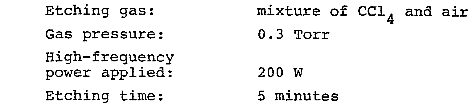
- A part of the chromium film in the photomask blank as prepared in Example 1 was removed by the dry etching method under the etching conditions shown below to produce a desired photomask.
-
- On a glass plate, a film of chromium was formed to a thickness of 50 A according to the electron-beam heated vacuum evaporation method, and then a film of silicon 0 oxide was formed to a thickness of 200 A according to the same method. Further, a tantalum film was formed on 0 the silicon oxide film to a thickness of 1,000 A according to the electron-beam heated vacuum evaporation method to obtain a desired photomask blank.
- A part of the tantalum film in the blank as prepared above was removed by etching according to the dry etching method under the following etching conditions to obtain a desired photomask.
-

- A part of the silicon film in the photomask blank as prepared in Example 4 was removed by etching according to the dry etching method under the following etching conditions to obtain a desired photomask.
-


- On a glass plate, a chromium film was formed to a 0 thickness of 50 A according to the electron-beam heating system vapor deposition method, and then a film of silicon oxide was formed thereon to a thickness of 200 0 A according to the same method. Further, on the silicon oxide film, a silicon film was formed to a thickness of 0 1,000 A to obtain a photomask blank.
- Following the procedures as described in Example 4, a part of the silicon film in the blank as prepared above was removed by etching to produce a desired photomask.
- A part of the silicon film in the blank as prepared in Example 8 was removed by etching according to the dry etching method under the following conditions.
-

- With the use of ten sheets for each of the photomasks as prepared in Examples 5 to 9, the chemical resistance test and the test with respect to electrostatic charges were conducted similarly as described in Example 3. As a result of the chemical resistance tests, no defect was found to have developed in any of the photomasks, without change in electroconductivity. Further, no defect was observed to be caused by electrostatic charges.
Claims (12)
Applications Claiming Priority (10)
| Application Number | Priority Date | Filing Date | Title |
|---|---|---|---|
| JP141565/80 | 1980-10-09 | ||
| JP14156580A JPS5764739A (en) | 1980-10-09 | 1980-10-09 | Photomask substrate and photomask |
| JP2872181A JPS57144549A (en) | 1981-02-28 | 1981-02-28 | Photomask |
| JP2872281A JPS57144550A (en) | 1981-02-28 | 1981-02-28 | Blank plate for photomask |
| JP28722/81 | 1981-02-28 | ||
| JP28721/81 | 1981-02-28 | ||
| JP68694/81 | 1981-05-07 | ||
| JP68693/81 | 1981-05-07 | ||
| JP6869381A JPS57182740A (en) | 1981-05-07 | 1981-05-07 | Photomask |
| JP6869481A JPS57182741A (en) | 1981-05-07 | 1981-05-07 | Photomask blank plate |
Publications (3)
| Publication Number | Publication Date |
|---|---|
| EP0049799A2 true EP0049799A2 (en) | 1982-04-21 |
| EP0049799A3 EP0049799A3 (en) | 1982-11-17 |
| EP0049799B1 EP0049799B1 (en) | 1986-02-12 |
Family
ID=27521064
Family Applications (1)
| Application Number | Title | Priority Date | Filing Date |
|---|---|---|---|
| EP81107702A Expired EP0049799B1 (en) | 1980-10-09 | 1981-09-28 | Photomask blank and photomask |
Country Status (2)
| Country | Link |
|---|---|
| EP (1) | EP0049799B1 (en) |
| DE (1) | DE3173769D1 (en) |
Cited By (9)
| Publication number | Priority date | Publication date | Assignee | Title |
|---|---|---|---|---|
| EP0054736A3 (en) * | 1980-12-22 | 1982-11-17 | Dai Nippon Insatsu Kabushiki Kaisha | Photomask and photomask blank |
| EP0542265A1 (en) * | 1991-11-15 | 1993-05-19 | Canon Kabushiki Kaisha | X-ray mask structure and x-ray exposing method, and semiconductor device manufactured by use of x-ray mask structure, and method for manufacturing x-ray mask structure |
| FR2694131A1 (en) * | 1992-07-21 | 1994-01-28 | Balzers Hochvakuum | Method and apparatus for manufacturing a component, in particular an optical component, and optical component thus obtained |
| CH686461A5 (en) * | 1992-07-21 | 1996-03-29 | Balzers Hochvakuum | Process for producing a component, optical component and system for carrying out the process. |
| CN102906850A (en) * | 2010-03-22 | 2013-01-30 | 迈普尔平版印刷Ip有限公司 | Lithography system, sensor, converter element and method of manufacture |
| CN102034752B (en) * | 2009-09-25 | 2013-07-17 | 台湾积体电路制造股份有限公司 | photolithographic patterning method |
| US9030675B2 (en) | 2010-11-13 | 2015-05-12 | Mapper Lithography Ip B.V. | Method for determining a distance between two beamlets in a multi-beamlet exposure apparatus |
| KR20180122312A (en) * | 2012-10-15 | 2018-11-12 | 클린 서피스 기쥬츠 가부시키가이샤 | Mask blank and photomask |
| US11143953B2 (en) | 2019-03-21 | 2021-10-12 | International Business Machines Corporation | Protection of photomasks from 193nm radiation damage using thin coatings of ALD Al2O3 |
Family Cites Families (5)
| Publication number | Priority date | Publication date | Assignee | Title |
|---|---|---|---|---|
| US3622319A (en) * | 1966-10-20 | 1971-11-23 | Western Electric Co | Nonreflecting photomasks and methods of making same |
| NL143620B (en) * | 1967-02-02 | 1974-10-15 | Nii Tochnoi T | METHOD OF COLORING A SURFACE OF AN OBJECT AND AN OBJECT WITH A SURFACE COLORED ACCORDING TO THIS METHOD. |
| JPS5323277A (en) * | 1976-08-14 | 1978-03-03 | Konishiroku Photo Ind Co Ltd | Photomasking material and photomask |
| JPS5340281A (en) * | 1976-09-27 | 1978-04-12 | Konishiroku Photo Ind Co Ltd | Photo mask material and manufacturtof it |
| US4178403A (en) * | 1977-08-04 | 1979-12-11 | Konishiroku Photo Industry Co., Ltd. | Mask blank and mask |
-
1981
- 1981-09-28 EP EP81107702A patent/EP0049799B1/en not_active Expired
- 1981-09-28 DE DE8181107702T patent/DE3173769D1/en not_active Expired
Cited By (12)
| Publication number | Priority date | Publication date | Assignee | Title |
|---|---|---|---|---|
| EP0054736A3 (en) * | 1980-12-22 | 1982-11-17 | Dai Nippon Insatsu Kabushiki Kaisha | Photomask and photomask blank |
| EP0542265A1 (en) * | 1991-11-15 | 1993-05-19 | Canon Kabushiki Kaisha | X-ray mask structure and x-ray exposing method, and semiconductor device manufactured by use of x-ray mask structure, and method for manufacturing x-ray mask structure |
| US5422921A (en) * | 1991-11-15 | 1995-06-06 | Canon Kabushiki Kaisha | X-ray mask structure and manufacturing methods including forming a metal oxide film on a portion of an X-ray permeable film having no X-ray absorber thereon |
| FR2694131A1 (en) * | 1992-07-21 | 1994-01-28 | Balzers Hochvakuum | Method and apparatus for manufacturing a component, in particular an optical component, and optical component thus obtained |
| CH686461A5 (en) * | 1992-07-21 | 1996-03-29 | Balzers Hochvakuum | Process for producing a component, optical component and system for carrying out the process. |
| US5667700A (en) * | 1992-07-21 | 1997-09-16 | Balzers Aktiengesellschaft | Process for the fabrication of a structural and optical element |
| CN102034752B (en) * | 2009-09-25 | 2013-07-17 | 台湾积体电路制造股份有限公司 | photolithographic patterning method |
| CN102906850A (en) * | 2010-03-22 | 2013-01-30 | 迈普尔平版印刷Ip有限公司 | Lithography system, sensor, converter element and method of manufacture |
| USRE47287E1 (en) | 2010-03-22 | 2019-03-12 | Mapper Lithography Ip B.V. | Lithography system, sensor, converter element and method of manufacture |
| US9030675B2 (en) | 2010-11-13 | 2015-05-12 | Mapper Lithography Ip B.V. | Method for determining a distance between two beamlets in a multi-beamlet exposure apparatus |
| KR20180122312A (en) * | 2012-10-15 | 2018-11-12 | 클린 서피스 기쥬츠 가부시키가이샤 | Mask blank and photomask |
| US11143953B2 (en) | 2019-03-21 | 2021-10-12 | International Business Machines Corporation | Protection of photomasks from 193nm radiation damage using thin coatings of ALD Al2O3 |
Also Published As
| Publication number | Publication date |
|---|---|
| DE3173769D1 (en) | 1986-03-27 |
| EP0049799A3 (en) | 1982-11-17 |
| EP0049799B1 (en) | 1986-02-12 |
Similar Documents
| Publication | Publication Date | Title |
|---|---|---|
| US4440841A (en) | Photomask and photomask blank | |
| US7387855B2 (en) | Anti-ESD photomask blank | |
| KR100280036B1 (en) | Photomask, its Fabrication Method and Modification Method with Phase-shift Layer | |
| CA1187203A (en) | Integrated circuit photomask | |
| US4556608A (en) | Photomask blank and photomask | |
| EP0049799B1 (en) | Photomask blank and photomask | |
| US3877810A (en) | Method for making a photomask | |
| US3542612A (en) | Photolithographic masks and methods for their manufacture | |
| JP3605567B2 (en) | Method for forming transparent conductive film using chemically amplified resist | |
| JPS62282445A (en) | Substrate for inspection and manufacture thereof | |
| JPS62218585A (en) | Production of photomask | |
| JP2984030B2 (en) | Substrate for photomask material, photomask material, and method for producing them | |
| KR100526527B1 (en) | Photomask and foaming mask pattern using the same | |
| JPS649617B2 (en) | ||
| JPS61240243A (en) | Photomask blank and photomask | |
| SU938338A1 (en) | Mask and method of manufacturing thereof | |
| JPS6322301B2 (en) | ||
| JPS6322299B2 (en) | ||
| JPH04318955A (en) | Glass board for dummy wafer | |
| Okada et al. | Approach to fabricating defect-free x-ray masks | |
| JP6767601B1 (en) | Photomask | |
| JPS6280655A (en) | Photomask blank and photomask | |
| JP2731914B2 (en) | Inspection board and manufacturing method thereof | |
| JPS6322300B2 (en) | ||
| JPS6322298B2 (en) |
Legal Events
| Date | Code | Title | Description |
|---|---|---|---|
| PUAI | Public reference made under article 153(3) epc to a published international application that has entered the european phase |
Free format text: ORIGINAL CODE: 0009012 |
|
| AK | Designated contracting states |
Designated state(s): CH DE FR |
|
| PUAL | Search report despatched |
Free format text: ORIGINAL CODE: 0009013 |
|
| AK | Designated contracting states |
Designated state(s): CH DE FR |
|
| 17P | Request for examination filed |
Effective date: 19830208 |
|
| RAP1 | Party data changed (applicant data changed or rights of an application transferred) |
Owner name: DAI NIPPON INSATSU KABUSHIKI KAISHA |
|
| GRAA | (expected) grant |
Free format text: ORIGINAL CODE: 0009210 |
|
| AK | Designated contracting states |
Designated state(s): CH DE FR LI |
|
| ET | Fr: translation filed | ||
| REF | Corresponds to: |
Ref document number: 3173769 Country of ref document: DE Date of ref document: 19860327 |
|
| PLBE | No opposition filed within time limit |
Free format text: ORIGINAL CODE: 0009261 |
|
| STAA | Information on the status of an ep patent application or granted ep patent |
Free format text: STATUS: NO OPPOSITION FILED WITHIN TIME LIMIT |
|
| 26N | No opposition filed | ||
| PGFP | Annual fee paid to national office [announced via postgrant information from national office to epo] |
Ref country code: CH Payment date: 19981009 Year of fee payment: 18 |
|
| PG25 | Lapsed in a contracting state [announced via postgrant information from national office to epo] |
Ref country code: LI Free format text: LAPSE BECAUSE OF NON-PAYMENT OF DUE FEES Effective date: 19990930 Ref country code: CH Free format text: LAPSE BECAUSE OF NON-PAYMENT OF DUE FEES Effective date: 19990930 |
|
| REG | Reference to a national code |
Ref country code: CH Ref legal event code: PL |
|
| PGFP | Annual fee paid to national office [announced via postgrant information from national office to epo] |
Ref country code: FR Payment date: 20000912 Year of fee payment: 20 |
|
| PGFP | Annual fee paid to national office [announced via postgrant information from national office to epo] |
Ref country code: DE Payment date: 20000918 Year of fee payment: 20 |