EP0051079B1 - Additionneur/soustracteur binaire parallèle en technique MOS à propagation des retenues et étage d'addition/soustraction approprié - Google Patents
Additionneur/soustracteur binaire parallèle en technique MOS à propagation des retenues et étage d'addition/soustraction approprié Download PDFInfo
- Publication number
- EP0051079B1 EP0051079B1 EP80106726A EP80106726A EP0051079B1 EP 0051079 B1 EP0051079 B1 EP 0051079B1 EP 80106726 A EP80106726 A EP 80106726A EP 80106726 A EP80106726 A EP 80106726A EP 0051079 B1 EP0051079 B1 EP 0051079B1
- Authority
- EP
- European Patent Office
- Prior art keywords
- adder
- subtracter
- stage
- input
- output
- Prior art date
- Legal status (The legal status is an assumption and is not a legal conclusion. Google has not performed a legal analysis and makes no representation as to the accuracy of the status listed.)
- Expired
Links
Images
Classifications
-
- G—PHYSICS
- G06—COMPUTING OR CALCULATING; COUNTING
- G06F—ELECTRIC DIGITAL DATA PROCESSING
- G06F7/00—Methods or arrangements for processing data by operating upon the order or content of the data handled
- G06F7/38—Methods or arrangements for performing computations using exclusively denominational number representation, e.g. using binary, ternary, decimal representation
- G06F7/48—Methods or arrangements for performing computations using exclusively denominational number representation, e.g. using binary, ternary, decimal representation using non-contact-making devices, e.g. tube, solid state device; using unspecified devices
- G06F7/50—Adding; Subtracting
- G06F7/505—Adding; Subtracting in bit-parallel fashion, i.e. having a different digit-handling circuit for each denomination
- G06F7/509—Adding; Subtracting in bit-parallel fashion, i.e. having a different digit-handling circuit for each denomination for multiple operands, e.g. digital integrators
-
- G—PHYSICS
- G06—COMPUTING OR CALCULATING; COUNTING
- G06F—ELECTRIC DIGITAL DATA PROCESSING
- G06F7/00—Methods or arrangements for processing data by operating upon the order or content of the data handled
- G06F7/38—Methods or arrangements for performing computations using exclusively denominational number representation, e.g. using binary, ternary, decimal representation
- G06F7/48—Methods or arrangements for performing computations using exclusively denominational number representation, e.g. using binary, ternary, decimal representation using non-contact-making devices, e.g. tube, solid state device; using unspecified devices
- G06F7/544—Methods or arrangements for performing computations using exclusively denominational number representation, e.g. using binary, ternary, decimal representation using non-contact-making devices, e.g. tube, solid state device; using unspecified devices for evaluating functions by calculation
-
- G—PHYSICS
- G06—COMPUTING OR CALCULATING; COUNTING
- G06F—ELECTRIC DIGITAL DATA PROCESSING
- G06F2207/00—Indexing scheme relating to methods or arrangements for processing data by operating upon the order or content of the data handled
- G06F2207/38—Indexing scheme relating to groups G06F7/38 - G06F7/575
- G06F2207/3804—Details
- G06F2207/3808—Details concerning the type of numbers or the way they are handled
- G06F2207/3832—Less usual number representations
- G06F2207/3836—One's complement
-
- G—PHYSICS
- G06—COMPUTING OR CALCULATING; COUNTING
- G06F—ELECTRIC DIGITAL DATA PROCESSING
- G06F2207/00—Indexing scheme relating to methods or arrangements for processing data by operating upon the order or content of the data handled
- G06F2207/38—Indexing scheme relating to groups G06F7/38 - G06F7/575
- G06F2207/3804—Details
- G06F2207/386—Special constructional features
- G06F2207/388—Skewing
Definitions
- the invention relates to binary MOS ripple carry parallel add / subtractors, which are integrated by means of insulating layer field effect transistors of the enhancement type, according to the features specified in the preamble of claim 1.
- binary MOS ripple carry parallel add / subtractors which are integrated by means of insulating layer field effect transistors of the enhancement type, according to the features specified in the preamble of claim 1.
- several numbers represented in the natural n-digit binary code should be able to be added up or subtracted from one another by successively adding up to form partial sums.
- the subtotals with the numbers A, B, C ... Z are based on the following recursive formula:
- Each subtotal is formed in a parallel adder / subtractor, which consists of an adder / subtractor for each digit of each subtotal.
- This in turn consists of a changeover element that takes the sign of the number into account, i.e. a changeover element for switching from adding to subtracting, with a first input for a corresponding changeover signal and with a second input for one of two position signals that serves as a subtractor the number.
- the adder / subtractor stage consists of a full adder, the first input of which is directly supplied with the position signal, which serves as a minuend in the case of subtraction, and the second input of which is at the output of the switching element.
- the invention solves the problem with a parallel adding / subtracting mechanism in MOS technology which operates on the principle of looping through the carry (ripple carry), in which in particular the so-called carry reset (carry save) (cf. pages 106 and 129 of the book mentioned) is realized in a particularly simple manner to multiply one of the signals to be summed up, that is to say for example one of the numbers or one of the partial sums already calculated, by a power of two.
- Such a stretching process occurs, for example, with digital filters.
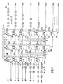
- Parallel adders / subtractors AB, AC, AZ are drawn, while for the arbitrary number of additional numbers to be added up between C and Z, the respective lines are dotted accordingly is indicated.
- Each adding / subtracting stage consists of the usual full adder VA and the switching element U, which can be constructed, for example, according to the circuit shown in FIG. 2. Because of the clarity of FIG. 1, the reference symbols VA and U are only entered in the add / subtract stage ABO.
- the position signals A0, BO of the lowest digit of the two numbers A, B are fed to the first input of the full adder VA and the second input of the changeover element U, the first input of which is supplied with the changeover signal originating from the changeover register UR.
- digital signals are stored which correspond to the signs of the individual numbers to be taken into account in the summation, specifically with the positive logic for addition, that is to say a plus sign, the low binary level L and for subtraction, that is to say for the exemplary embodiment in FIG. 1 the minus sign, the high binary level H.
- the first input of the full adder of the adder / subtractor stage ACO is supplied with the position signal CO of the number C, while its carry input and the first input of the associated switching element are supplied with the corresponding switching signal.
- the sum signal ScO arises, which, if the corresponding connecting line is thought to be fully excellent, is fed to the second input of the switching element of the adder / subtractor stage AZO.
- the position signal ZO of the number Z is fed to the first input of the full adder belonging to the adding / subtracting stage AZO, while the corresponding switching signal is in turn present at the carry input of this full adder and at the first input of the associated switching element.
- the sum signal SzO thus arises at the sum output of this full adder.
- Each subsequent parallel add / subtractor is to be expanded by a further add / subtract stage in the manner described, so that finally the parallel add / subtractor AZ zn-2 has further add / subtract stages, of which those with the reference symbols AZn and AZx in Fig. 1 are shown.
- the position signals A1, B1 to be summed only appear at the point in time at which the carry signal from the adder / subtractor stage ABO processing the lowest position signals A0, BO also appears is available.
- the most significant position signals Am, Bm are therefore only available at the inputs of the most significant adding / subtracting stage ABm when the carry signal from the preceding adding / subtracting stage also occurs at their carry input. In contrast to the known prior art, it is therefore not necessary to provide special stages for the carry reset.
- the number of delay elements V increases by one with increasing significance of the position signals, now according to a further essential feature of the invention, similar delay elements V must also be provided on the output side, but the number increases as the number increases The value of the output point signals decreases by one.
- the most significant adder / subtractor AZx of the parallel adder / subtractor AZ thus has no delay element V like the least significant adder / subtractor ABO of the parallel adder / subtractor AB, i. H. its output providing the sum signal Szx is connected directly to the output SAx of the sum output SA.
- the next lower adder / subtractor stage which is not shown in FIG.
- the delay elements V inserted into the output circuit in accordance with the invention ensure that the individual position signals occur at the sum output SA at the same time, ie. H. at the same time the output binary word is available in parallel.
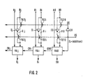
- FIG. 2 shows some adding / subtracting stages which can be used advantageously in the invention and thus also in the exemplary embodiment according to FIG. 1. These are the stages labeled with the running numbers 0, i, j, which in turn consist of the corresponding full adders VAO, VAi, VAj and the associated switching elements U0, Ui, Uj.
- the structure of the full adders is not specified in detail in FIG. 2, which should mean that conventional full adder circuits can be provided for this.
- the switching elements U0, Ui, Uj are constructed in the same way and consist of the inverter 10, li, lj, the input of which lies at the second input of the switching element, that is to say at the input to which the subtrahend is fed in in the event of subtraction.
- the position signals BO, Bi, Bj are fed to this second input in FIG. 2.
- Each switching element U0, Ui, Uj also consists of the first transfer element TG10, TG1 i, TG1j, which is arranged with its signal path between the inverter output and the switching element output.
- the second transfer element TG20, TG2i, TG2j is also provided for each changeover element U0, Ui, Uj, which lies with its signal path between the second changeover element input and the changeover element output.
- the signal paths of the two transfer elements TG10, TG20 or TG1 i, TG2i, or TG1j, TG2j are connected to each other at the changeover element output and thus also at the second full adder input, while the other end of the second transfer element TG20, TG2i, TG2j (Subtrahend) position signal BO, Bi, Bj is supplied.
- the control inputs of the first transfer elements TG10, TG1 i, TG1j are connected to one another, and they are supplied with the switchover signal US, which, as already mentioned, must have the lower binary signal L in the case of addition in the positive logic.
- control inputs of the second transfer elements TG20, TG2i, TG2j are also connected to one another, and the switchover signal US inverted via the common inverter IV is fed to them.
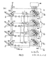
- FIG. 3 shows how one of the partial sums or one of the numbers is to be multiplied by a factor which is a power of two with predetermined exponents q. This requirement occurs, for example, in the case of parallel adding / subtracting units to be used in digital filters.
- the power of two multiplication can be implemented particularly advantageously with the aid of the transfer elements also shown for the switching elements with reference to FIG. 2.
- Fig. 3 it is shown how by means of the add / subtract stages VAIO VAI1, VAI2, VAI3 forming the partial sum SI, the number L and the preceding partial sum Sk are added so that the equation is fulfilled. It is therefore a prerequisite for the specific exemplary embodiment in FIG. 3 that the partial sum Sk and also the number L have four digits.
- the switching elements UIO, U11, U12, U13 are shown which consist of the inverters 110, 111, 112, 113, the first transfer elements TG10, TG11, TG12, TG13 and the second transfer elements TG20, TG21, TG22 , TG23 exist. Furthermore, the common inverter IVI is shown, to which the switchover signal US is fed, which is also connected to the carry input of the least significant full adder VA10.
- Two further delay elements V are now connected in series between the outputs of the switching elements U10 ... U13 and the corresponding full adder input, one of which is located at the output of the switching elements U10 ... U13.
- the signal path of the transfer stage TS03, TS13, TS23, TS33 assigned to the two-exponent zero is also inserted.
- each full adder input there are further transfer stages TS01, TS02, TS04, TS05 or TS11, TS12, TS14, TS15 or TS21, TS22, TS24, TS25 or TS31, TS32, TS34, TS35 for each positive and negative two-digit exponent that is different from zero .
- these are assigned the powers of two 2- 2 , 2- 1 , 2 1 , 2 2 provided therein that the transfer elements with the end-of-reference number 1 to 2- 2 , those with the end number 2 to 2- 1 , with the Final digit 4 to 2 1 and those with the final digit 5 to 2 2 belong.
- the control inputs of the transfer stages TS ... are connected to corresponding binary signals, which are stored in the multiplier register MR accordingly.
- the other end of the signal paths of the transfer stages TS ... which do not belong to the power of two 2 °, is now at corresponding circuit points in higher or lower order stages.
- the transfer stages TS ... 2 belonging to the first negative exponent 2- 1 i.e. the other end of their signal path, are connected at the connection point of the penultimate and the last delay element V for the next higher position signals, the counting direction for the further delay elements V in FIG 3 applies from left to right.
- the transfer stage TS02 (belongs to the lowest valency 0) is located at the connection point of the two delay elements V in the line below, which belongs to the valency 1.
- the transfer stage TS12 is located at the connection point of the delay elements V belonging to the line below it with the value 2.
- the transfer stages belonging to the second negative exponent 2 - 2 with the reference numeral 1 it applies that they are connected to a delay element V in a line processing second higher position signals or, if this line is not present, are also to be fed with the switchover signal US.
- the transfer stage TS01 according to FIG. 3 is located at the input of the first delay element V in the next but one line belonging to the valency 2.
- the transfer stage TS11 in the row with the significance 1 is connected to the input of the first delay element V in the row with the significance 3, while the transfer stages TS21, TS31 are connected to the switchover signal US.
- the transfer stage TS34 is located at the connection point of the two delay elements V in the next lower line belonging to the value 2, correspondingly the transfer stage TS24 from this line at the connection point of the two delay elements V in the line with the value 1 and correspondingly also the transfer stage TS14 from this Line at the corresponding point in the line with the value 0, while the transfer stage TS04 of this lowest line is in turn connected to the switchover signal US.
- the transfer stages TS ... By means of the transfer stages TS ... a power of two multiplication is realized by shifting the position within the binary word, which is known per se. If such a multiplication is to take place, the corresponding transfer stages TS ... are conductively controlled by the H signal correspondingly present with the presupposed positive logic and thus the position signals originating from other lines are fed to the corresponding full adder VAI ...
- the advantages of the invention are particularly advantageous, since the above-described mode of operation, to deliver all position signals at the output at a certain point in time, is therefore well tolerated.
- “With regard to the signal flow two-phase clocked” is intended here to mean that the MOS circuit itself can be implemented according to the principles of static ratio switching technology, but that transfer transistors alternately clocked by the two clock signals are arranged in front of input points and after output points.
- the two clock signals are square-wave voltages with the pulse duration-pulse pause ratio 1: 1, which are 180 ° out of phase with one another.
- the timing of the transfer transistors is generally carried out in such a way that if the transfer transistor assigned to an input of a particular stage is controlled by one clock signal, the transfer transistor assigned to the output of this stage is then controlled by the other clock signal.
- a conventional inverter is provided according to this principle with an input transfer transistor and an output transfer transistor, which are controlled by the two clock signals, the delay between the signal input located in front of the input transfer transistor and the signal output located behind the output transfer transistor exactly half the period of the clock signals.
- each delay element V should namely be equal to the time required for the carry-over formation of a full adder VA.
- they can thus be implemented by the inverter just described with upstream and downstream transfer transistors, so that they then have half the period of the two clock signals as the delay time.
- the parallel adder / subtractor according to the invention can be integrated by means of MOS transistors of the same type of line, that is to say either in P-channel or N-channel technology, and it can be advantageous to convert the load transistors of inverters and logic elements in the form of depletion type transistors , that is, as so-called depletion load elements.
- the parallel adding / subtracting unit by means of MOS transistors of complementary line types, that is to say in the so-called CMOS or COSMOS technology.
- the transfer elements and stages are CMOS transmission gates.
Landscapes
- Engineering & Computer Science (AREA)
- Physics & Mathematics (AREA)
- General Physics & Mathematics (AREA)
- Theoretical Computer Science (AREA)
- Computational Mathematics (AREA)
- Mathematical Analysis (AREA)
- Pure & Applied Mathematics (AREA)
- Computing Systems (AREA)
- Mathematical Optimization (AREA)
- General Engineering & Computer Science (AREA)
- Compression, Expansion, Code Conversion, And Decoders (AREA)
Claims (6)
Priority Applications (4)
| Application Number | Priority Date | Filing Date | Title |
|---|---|---|---|
| EP80106726A EP0051079B1 (fr) | 1980-11-03 | 1980-11-03 | Additionneur/soustracteur binaire parallèle en technique MOS à propagation des retenues et étage d'addition/soustraction approprié |
| DE8080106726T DE3069310D1 (en) | 1980-11-03 | 1980-11-03 | Binary mos ripple carry parallel adder/subtractor and appropriate adding/subtracting stage |
| JP56175872A JPS57106954A (en) | 1980-11-03 | 1981-11-04 | Binary metal oxide semiconductor ripple-carry parallel adder/subtracter and addition/subtraction column proper to said apparatus |
| US06/780,226 US4683548A (en) | 1980-11-03 | 1985-09-24 | Binary MOS ripple-carry parallel adder/subtracter and adder/subtracter stage suitable therefor |
Applications Claiming Priority (1)
| Application Number | Priority Date | Filing Date | Title |
|---|---|---|---|
| EP80106726A EP0051079B1 (fr) | 1980-11-03 | 1980-11-03 | Additionneur/soustracteur binaire parallèle en technique MOS à propagation des retenues et étage d'addition/soustraction approprié |
Publications (2)
| Publication Number | Publication Date |
|---|---|
| EP0051079A1 EP0051079A1 (fr) | 1982-05-12 |
| EP0051079B1 true EP0051079B1 (fr) | 1984-09-26 |
Family
ID=8186869
Family Applications (1)
| Application Number | Title | Priority Date | Filing Date |
|---|---|---|---|
| EP80106726A Expired EP0051079B1 (fr) | 1980-11-03 | 1980-11-03 | Additionneur/soustracteur binaire parallèle en technique MOS à propagation des retenues et étage d'addition/soustraction approprié |
Country Status (4)
| Country | Link |
|---|---|
| US (1) | US4683548A (fr) |
| EP (1) | EP0051079B1 (fr) |
| JP (1) | JPS57106954A (fr) |
| DE (1) | DE3069310D1 (fr) |
Families Citing this family (16)
| Publication number | Priority date | Publication date | Assignee | Title |
|---|---|---|---|---|
| JPS58137381A (ja) * | 1982-02-10 | 1983-08-15 | Sony Corp | デイジタルカラ−エンコ−ダ |
| US4744043A (en) * | 1985-03-25 | 1988-05-10 | Motorola, Inc. | Data processor execution unit which receives data with reduced instruction overhead |
| JPS61267829A (ja) * | 1985-05-23 | 1986-11-27 | Mitsubishi Electric Corp | ビツト分割型同期式累算器 |
| US4709226A (en) * | 1985-07-15 | 1987-11-24 | Rca Corporation | Circuitry for complementing binary numbers |
| US4887233A (en) * | 1986-03-31 | 1989-12-12 | American Telephone And Telegraph Company, At&T Bell Laboratories | Pipeline arithmetic adder and multiplier |
| JPH02259926A (ja) * | 1989-03-31 | 1990-10-22 | Hitachi Ltd | 加算制御方式 |
| GB2230361B (en) * | 1989-04-07 | 1993-02-10 | Sony Corp | Binary adding apparatus |
| JPH03113632A (ja) * | 1989-09-28 | 1991-05-15 | Nec Corp | ディジタル信号処理装置 |
| US5161119A (en) * | 1990-02-14 | 1992-11-03 | Lsi Logic Corporation | Weighted-delay column adder and method of organizing same |
| EP0452517A1 (fr) * | 1990-03-20 | 1991-10-23 | Siemens Aktiengesellschaft | Comparateur de deux sommes |
| EP0571694B1 (fr) * | 1992-05-27 | 1995-12-06 | STMicroelectronics S.r.l. | Chaîne additionneuse rapide |
| MY114769A (en) * | 1994-04-18 | 2003-01-31 | Aviron Inc | Non-splicing variants of gp350/220 |
| JP3330236B2 (ja) * | 1994-09-01 | 2002-09-30 | 三菱電機エンジニアリング株式会社 | 加算回路およびキャリー選択回路 |
| KR100197354B1 (ko) * | 1995-06-28 | 1999-06-15 | 김영환 | 클럭 위상을 이용한 캐리증가 가산기 |
| US6119141A (en) * | 1998-05-06 | 2000-09-12 | Integrated Device Technology, Inc. | Resistive decoupling of function selection signals from input multiplexers in arithmetic logical units ALU |
| US6990509B2 (en) * | 2002-03-08 | 2006-01-24 | International Business Machines Corporation | Ultra low power adder with sum synchronization |
Family Cites Families (9)
| Publication number | Priority date | Publication date | Assignee | Title |
|---|---|---|---|---|
| GB1088354A (en) * | 1965-06-01 | 1967-10-25 | Int Computers & Tabulators Ltd | Improvements in or relating to electronic adders |
| US3535502A (en) * | 1967-11-15 | 1970-10-20 | Ibm | Multiple input binary adder |
| US3636334A (en) * | 1969-01-02 | 1972-01-18 | Univ California | Parallel adder with distributed control to add a plurality of binary numbers |
| US3603776A (en) * | 1969-01-15 | 1971-09-07 | Ibm | Binary batch adder utilizing threshold counters |
| US3602705A (en) * | 1970-03-25 | 1971-08-31 | Westinghouse Electric Corp | Binary full adder circuit |
| NL7712367A (nl) * | 1977-11-10 | 1979-05-14 | Philips Nv | Digitaal optelrekenorgaan. |
| FR2441214A1 (fr) * | 1978-11-13 | 1980-06-06 | Labo Cent Telecommunicat | Additionneur numerique |
| FR2454136B1 (fr) * | 1979-04-12 | 1985-12-06 | Materiel Telephonique | Additionneur sequentiel rapide |
| US4369500A (en) * | 1980-10-20 | 1983-01-18 | Motorola Inc. | High speed NXM bit digital, repeated addition type multiplying circuit |
-
1980
- 1980-11-03 EP EP80106726A patent/EP0051079B1/fr not_active Expired
- 1980-11-03 DE DE8080106726T patent/DE3069310D1/de not_active Expired
-
1981
- 1981-11-04 JP JP56175872A patent/JPS57106954A/ja active Pending
-
1985
- 1985-09-24 US US06/780,226 patent/US4683548A/en not_active Expired - Fee Related
Also Published As
| Publication number | Publication date |
|---|---|
| JPS57106954A (en) | 1982-07-03 |
| EP0051079A1 (fr) | 1982-05-12 |
| US4683548A (en) | 1987-07-28 |
| DE3069310D1 (en) | 1984-10-31 |
Similar Documents
| Publication | Publication Date | Title |
|---|---|---|
| EP0051079B1 (fr) | Additionneur/soustracteur binaire parallèle en technique MOS à propagation des retenues et étage d'addition/soustraction approprié | |
| EP0086904B1 (fr) | Circuit digital de calcul en parallèle pour des nombres binaires positifs et négatifs | |
| DE4101004C2 (de) | Paralleler Multiplizierer mit Sprungfeld und modifiziertem Wallac-Baum | |
| DE2018452A1 (de) | Arithmetische Einrichtung | |
| DE3036747A1 (de) | Binaere multiplikationszellenschaltung | |
| DE2007353B2 (de) | Vielstelliges addierwerk | |
| DE4403917A1 (de) | Vorrichtung zum Berechnen einer Besetzungszählung | |
| DE3940897C2 (de) | Schaltungsanordnung und Verfahren zur Berechnung digitaler Summen in einem Halbleiteraddierer mit Parallelübertrag | |
| DE1549508C3 (de) | Anordnung zur Übertragsberechnung mit kurzer Signallaufzeit | |
| DE3524981A1 (de) | Anordnung mit einem saettigbaren carry-save-addierer | |
| DE3434777C2 (fr) | ||
| EP0130397B1 (fr) | Appareil de calcul numérique | |
| EP0208275B1 (fr) | Dispositif d'addition parallèle par bit de nombres binaires | |
| DE3880825T2 (de) | Anordnung zur schnellen addition von binärzahlen. | |
| DE2017132A1 (de) | Binarer Parallel Addierer | |
| DE10117041C1 (de) | Carry-Ripple Addierer | |
| DE1512606A1 (de) | Verknuepfungsbaustein | |
| DE1424928B1 (de) | Schaltungsanordnung zum Addieren von durch binaere Signale dargestellten digitalen Informationen | |
| DE1109422B (de) | Asynchrone binaere Additions- und Subtraktionseinrichtung | |
| DE10139099C2 (de) | Carry-Ripple Addierer | |
| DE2902488C2 (fr) | ||
| EP0188779A1 (fr) | Multiplieur numérique rapide | |
| DE2737483A1 (de) | Korrektur-schaltungsanordnung fuer additions- oder substraktionsoperationen mit nicht-hexadezimalen operanden in hexadezimalen rechenwerken | |
| DE1803607C3 (de) | Schaltungsanordnung zur Umsetzung einer Dualzahl in eine im BCD Kode ver schlüsselte Dezimalzahl | |
| DE10130484A1 (de) | 7-zu-3 Bit Carry-Save Addierer |
Legal Events
| Date | Code | Title | Description |
|---|---|---|---|
| PUAI | Public reference made under article 153(3) epc to a published international application that has entered the european phase |
Free format text: ORIGINAL CODE: 0009012 |
|
| 17P | Request for examination filed |
Effective date: 19811010 |
|
| AK | Designated contracting states |
Designated state(s): DE FR GB IT NL |
|
| ITF | It: translation for a ep patent filed | ||
| GRAA | (expected) grant |
Free format text: ORIGINAL CODE: 0009210 |
|
| AK | Designated contracting states |
Designated state(s): DE FR GB IT NL |
|
| REF | Corresponds to: |
Ref document number: 3069310 Country of ref document: DE Date of ref document: 19841031 |
|
| PGFP | Annual fee paid to national office [announced via postgrant information from national office to epo] |
Ref country code: DE Payment date: 19841220 Year of fee payment: 5 |
|
| PGFP | Annual fee paid to national office [announced via postgrant information from national office to epo] |
Ref country code: FR Payment date: 19841227 Year of fee payment: 5 |
|
| ET | Fr: translation filed | ||
| PLBI | Opposition filed |
Free format text: ORIGINAL CODE: 0009260 |
|
| 26 | Opposition filed |
Opponent name: PHILIPS PATENTVERWALTUNG GMBH Effective date: 19850625 |
|
| NLR1 | Nl: opposition has been filed with the epo |
Opponent name: PHILIPS PATENTVERWALTUNG GMBH |
|
| PG25 | Lapsed in a contracting state [announced via postgrant information from national office to epo] |
Ref country code: GB Effective date: 19871103 |
|
| PGFP | Annual fee paid to national office [announced via postgrant information from national office to epo] |
Ref country code: NL Payment date: 19871130 Year of fee payment: 8 |
|
| GBPC | Gb: european patent ceased through non-payment of renewal fee | ||
| RDAG | Patent revoked |
Free format text: ORIGINAL CODE: 0009271 |
|
| STAA | Information on the status of an ep patent application or granted ep patent |
Free format text: STATUS: PATENT REVOKED |
|
| 27W | Patent revoked |
Effective date: 19881125 |
|
| GBPR | Gb: patent revoked under art. 102 of the ep convention designating the uk as contracting state | ||
| NLR2 | Nl: decision of opposition | ||
| APAH | Appeal reference modified |
Free format text: ORIGINAL CODE: EPIDOSCREFNO |