EP0051290A2 - Analysator für von einem Verbrennungsmotor erzeugte Wellenformen - Google Patents
Analysator für von einem Verbrennungsmotor erzeugte Wellenformen Download PDFInfo
- Publication number
- EP0051290A2 EP0051290A2 EP81109300A EP81109300A EP0051290A2 EP 0051290 A2 EP0051290 A2 EP 0051290A2 EP 81109300 A EP81109300 A EP 81109300A EP 81109300 A EP81109300 A EP 81109300A EP 0051290 A2 EP0051290 A2 EP 0051290A2
- Authority
- EP
- European Patent Office
- Prior art keywords
- signal
- waveform
- points
- analyzer
- ignition
- Prior art date
- Legal status (The legal status is an assumption and is not a legal conclusion. Google has not performed a legal analysis and makes no representation as to the accuracy of the status listed.)
- Withdrawn
Links
- 230000008439 repair process Effects 0.000 claims abstract description 25
- 238000005259 measurement Methods 0.000 claims abstract description 22
- 238000002485 combustion reaction Methods 0.000 claims abstract description 14
- 238000012545 processing Methods 0.000 claims abstract description 14
- 238000005070 sampling Methods 0.000 claims abstract description 12
- 238000012423 maintenance Methods 0.000 claims abstract description 9
- 230000002093 peripheral effect Effects 0.000 claims abstract description 4
- 238000010304 firing Methods 0.000 claims description 16
- 230000003750 conditioning effect Effects 0.000 claims description 11
- 238000012935 Averaging Methods 0.000 claims description 10
- 238000000034 method Methods 0.000 claims description 10
- 230000001143 conditioned effect Effects 0.000 claims description 9
- 238000003745 diagnosis Methods 0.000 claims description 9
- 230000008569 process Effects 0.000 claims description 8
- 239000003990 capacitor Substances 0.000 claims description 6
- 239000004020 conductor Substances 0.000 claims description 3
- 238000001514 detection method Methods 0.000 claims description 3
- 230000002238 attenuated effect Effects 0.000 abstract description 4
- 230000008859 change Effects 0.000 abstract description 2
- 238000010586 diagram Methods 0.000 description 27
- 238000012360 testing method Methods 0.000 description 26
- 239000000523 sample Substances 0.000 description 14
- 230000006870 function Effects 0.000 description 9
- 238000007493 shaping process Methods 0.000 description 7
- 241000282414 Homo sapiens Species 0.000 description 4
- 238000004088 simulation Methods 0.000 description 4
- 230000010355 oscillation Effects 0.000 description 3
- 238000004364 calculation method Methods 0.000 description 2
- 238000011084 recovery Methods 0.000 description 2
- 230000001360 synchronised effect Effects 0.000 description 2
- 230000000007 visual effect Effects 0.000 description 2
- 238000013459 approach Methods 0.000 description 1
- 230000008878 coupling Effects 0.000 description 1
- 238000010168 coupling process Methods 0.000 description 1
- 238000005859 coupling reaction Methods 0.000 description 1
- 230000007423 decrease Effects 0.000 description 1
- 230000003247 decreasing effect Effects 0.000 description 1
- 230000003111 delayed effect Effects 0.000 description 1
- 230000000994 depressogenic effect Effects 0.000 description 1
- 239000000446 fuel Substances 0.000 description 1
- 238000011835 investigation Methods 0.000 description 1
- 230000002459 sustained effect Effects 0.000 description 1
Images




Classifications
-
- F—MECHANICAL ENGINEERING; LIGHTING; HEATING; WEAPONS; BLASTING
- F02—COMBUSTION ENGINES; HOT-GAS OR COMBUSTION-PRODUCT ENGINE PLANTS
- F02P—IGNITION, OTHER THAN COMPRESSION IGNITION, FOR INTERNAL-COMBUSTION ENGINES; TESTING OF IGNITION TIMING IN COMPRESSION-IGNITION ENGINES
- F02P17/00—Testing of ignition installations, e.g. in combination with adjusting; Testing of ignition timing in compression-ignition engines
- F02P17/02—Checking or adjusting ignition timing
- F02P17/04—Checking or adjusting ignition timing dynamically
- F02P17/08—Checking or adjusting ignition timing dynamically using a cathode-ray oscilloscope
Definitions
- This invention relates to waveform analysis for internal combustion engine ignition waveforms and more particularly to such analysis which includes as a result specific repair and maintenance instructions for the analyzer operator.
- the invention disclosed herein relates to an internal combustion engine wave characteristic analyzer for a two dimensional wave signal wherein predetermined wave characteristic data are held in storage.
- Means is provided for receiving the ignition wave signal and for providing a plurality of sampled output signals corresponding to wave characteristics at a plurality of positions along the wave.
- Means is also provided for receiving and storing data indicative of said plurality of output signals together with means for continuously performing an analysis of the waveform utilizing ones of said plurality of output signal data, others of said plurality of output signal data and ones of said predetermined ignition wave characteristic data.
- the continuous analysis provides a discrete analysis signal which is coupled to means for continuously receiving and diagnosing said discrete analysis signal ana for providing a diagnostic signal responsive thereto.
- Means is coupled to said diagnostic signal for providing an instruction output relating to operations required to retain and reestablish the predetermined wave characteristic.
- Means is also provided for displaying alphanumeric instructions for an operator of the analyzer.
- This invention al-so related to an analyzer for use by an operator in determining deviations from normal characteristics of a two dimensional wavefoim signal which is produced by a machine wherein the waveform signal has a substantially predetermined shape for normal operation of the machine.
- Means is provided for receiving and for conditioning the waveform signal.
- Means is coupled to said means for receiving for sampling said conditioned waveform signal and for providing data signals resulting therefrom.
- Means is also provided for continuously processing said data signals, for continuously controlling said means for receiving and conditioning, and for continuously diagnosing said data signals with reference to the normal operation of the machine and others of said data signals.
- Means for interpreting said diagnosis is provided along with means for generating instructions for appropriate repairs to maintain and reestablish the normal machine operation.
- Means for communicating the instructions to the operator is also provided.
- Figure 1 depicts a system wherein the invention disclosed herein may be utilized.
- the system of Figure 1 relates to an internal combustion engine analyzer wherein digital data acquisition and digital data processing functions are performed under the control of a central processing unit included in a general purpose system 11.
- the data acquisition and data processing functions are controlled by the processor to be synchronous with the operation of an internal combustion engine being diagnosed.
- the manner in which the system is synchronized with the engine under test may be as described in U.S. Patent 3,619,676, Pelta et al.
- the processor also cooperates with a waveform analysis subsystem 12 which operates to receive engine and engine peripheral equipment generated waveform input signals.
- the waveform analysis subsystem is controlled by the processor to extract appropriate data from the input waveform.
- FIG. 2 is a block diagram depicting the waveform analysis subsystem 12 in greater detail and showing some of the input signals of interest.
- An ignition probe 13 provides the primary and secondary ignition waveforms generated by a conventional automotive ignition system including a distributor with mechanical ignition points, coil, condensor, spark plugs and interconnecting electrical conductors.
- a general purpose input 14 is available whereby a waveform such as the diode outputs in a vehicle alternator circuit or signals related to engine fuel injectors are introduced to the waveform analysis subsystem.
- a magnetic pickup input 16 is shown wherein an angular reference signal may be provided for every 360° rotation of the engine crank shaft.
- An expansion position 17 is provided for additional wavetorm inputs wherein the analysis of such waveforms may be of interest.
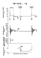
- FIG. 4 An engine ignition primary voltage waveform 18 is shown together with an ignition secondary voltage waveform 19. Also shown on the diagram of Figure 4 is a representative magnetic pickup signal 21.
- the magnetic pickup signal may or may not be in phase with one of the ignition waveforms as shown, as long as its relative phase position is known to the system.
- Figure 2 shows an electromagnetic interference attenuation and buffer section 22 to which the engine generated waveforms are initially coupled.
- the signals are subsequently connected to an analog processing section 23 which is coupled through an input-output circuit 24 to a processor 26.
- the processor contains the usual random access and read only memory, clock and central processing unit as indicated in Figure 2.
- Circuitry 27 performing an analog signal conditioning function is shown receiving the signals from the signal sources such as the signal sources 13, 14, 16 and 17 shown in Figure 2. Such circuitry is generally attenuation circuitry for reducing the signal levels from the signal sources to some extent so that they may be accepted by the subsequent analog circuitry.
- the initially conditioned secondary ignition wave (waveform 19 in Figure 4) is coupled to a secondary wave shaping circuit section 28 under the control of the processor 26 wherein the peak of the secondary wave is detected and transmitted in forms to be hereinafter described to a main multiplexer 29.
- the analog signal conditioning circuit also transmits directly certain of the input signals to the main multiplexer.
- the main multiplexer is also controlled by the processor so that predetermined ones of the inputs thereto are transmitted therethrough to a main gain control section 31.
- the main gain control is also subject to processor control, as will be hereinafter described, providing a properly adjusted analog signal-to an analog to digital (A/D) converter 32.
- the A/D converter is processor controlled.
- the output from the A/D converter is transmitted to the processor 26 as digitized data indicative of signal magnitudes for the input signals coupled thereto through the main multiplexer 29.
- a processor controlled duty cycle control section 33 produces an output which is presented at an input to the main multiplexer.
- the conditioned analog input signals are also transmitted to a secondary multiplexer 34 which is controlled by the processor 26.
- the adjusted analog signal from the main gain control 31 is coupled to the secondary multiplexer and a number two threshold detector 36 through a switching function associated with the secondary multiplexer.
- the number two threshold detector receives signals from a simulation signal generator 37 so that a certain amount of hysteresis may be imposed on the threshold detector output for purposes to be hereinafter described.
- the output of the number two threshold detector is a binary signal having one state for input signals which exceed the reference input and another state for signals which do not exceed the reference input.
- the conditioned analog signals are transmitted through the secondary multiplexer 34 together with the adjusted signal from the main gain control 31 under control of the processor 26 to a secondary gain control 38.
- the secondary gain control has an adjustable gain feature which is determined by the processor 26 so that the multiplexed signal is presented at the input of a number one threshold detector.39.
- the number one threshold detector also receives signals from the simulation signal generator 37 so that the detector output displays hysteresis in the fashion of the output from the threshold detector number two.
- the output of the number one threshold detector is coupled to the duty cycle control 33 which is enabled by the processor 26 to provide a duty cycle output to the main multiplexer 29.
- the number one threshold detector output is also a binary output similar to that of number two threshold detector. Both threshold detector outputs are coupled to the processor 26 as data.
- the secondary wave 19 may be seen in Figure 4 to be a positive going wave at tl and is presented in the drawing with such a characteristic because it is the more familiar depiction of the wave to those of skill in this field.
- the secondary wave appears at the input to the secondary wave shaping circuit 28 as a negative going wave thereby appearing as the mirror image about the abscissa of the waveform 19 in Figure 4.
- the circuit 28 as seen in Figure 5 is constructed to accept the negative going conditioned secondary waveform and the operation of the circuit hereinafter will be described in terms of the negative going signal. It will be apparent to those of skill in this art that the waveform may be of either polarity without effecting the concepts disclosed herein for wave shaping.
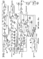
- the secondary wave shaping circuit 28 is seen in the upper portion of Figure 5 wherein the conditioned analog secondary wave (waveform 19 in Figure 4) is coupled to the input of a differentiating circuit including capacitor Cl and resistors Rl and R2.
- the differentiating circuit provides a first derivative of the waveform 19 at the inverting input of a comparator Al.
- the comparator is set so that a reference voltage at the noninverting input thereof is determined by the resistors R3 through R5 and the level of minus V.
- the reference may be conveniently set at minus 0.20 volts in this example.
- the conditioned secondary wave has a slope steep enough to provide a first derivative in excess of the reference voltage only in the area of the firing pulse indicated at tl in Figure 4.
- the comparator output is low in the "waiting" mode in this embodiment.
- a switch S19 is held on by the comparator “waiting” (low) output.
- An output from the comparator Al is produced (high state) when the first derivative level exceeds the reference level.
- the switch S19 is turned off by the high state from the comparator, removing the ground from the junction of R5 and R6 and providing a new (less negative) minus 0.05 volt reference for the comparator due to the configuration of the resistor network R3 through R6 and the combination of -V and +V.
- the comparator output also is coupled to one of the inputs of an AND gate A2.
- an output from the processor 26 is provided to an OR gate A20 which provides an enabling signal to another input on the AND gate A2 so that an output is provided therefrom.
- the negative going secondary wave provides a continuing output from the comparator Al until the rate of change of the secondary wave becomes less than minus 0.05 volts (approaches zero).
- the conditioned secondary waves occur in series, cylinder by cylinder, at the input to the circuit 28.
- an output from the AND gate A2 is obtained for a preselected secondary wave by energizing the OR gate A20 with a signal from the processor 26.
- the OR gate output enables gate A2.
- the output from gate A2 is connected to a holdover one shot device 41 which provides an output pulse which is sustained during the time A2 provides an output and after the end of the pulse from the AND gate A2.
- the one shot output is coupled to another input at the OR gate A20 so that the AND gate A2 is enabled either by the processor or by the one shot output.
- the OR gate and switch S19 therefore operate to reject noise in the secondary waveform.
- the output from the holdover one shot device 41 shown in Figure 5 is also coupled to the processor 26 provide an indication of the occurrence of a firing pulse for a cylinder.
- the one shot signal is also coupled to the actuating terminal of an electronic switch S2 and through an inverter A3 to the actuating terminal of an electronic switch Sl.
- the circuitry is such that in the presence of the holdover one shot pulse switch Sl is open and switch S2 is closed. In the absence of such a pulse Sl is closed and S2 is open.
- the preconditioned secondary wave is also coupled to the noninverting input of an amplifier A4. As mentioned hereinbefore the secondary wave is actually a mirror image (negative going) of the waveform 19 seen in Figure 4 for the purposes of description of the circuit of Figure 5.
- the main multiplexer 29 has connected thereto the input signals from the various engine characteristic sensors after those signals have been passed through the electromagnetic interference and buffer section 22 ( Figure 2).
- Main multiplexer 29 may be seen to be under the control of the processor 26 so that selected ones of the buffered input signals are provided to the noninverting input of a subsequent buffer amplifier A7.
- a series of switches S3 through S7 may be seen to be controlled by the processor 26 whereby actuation of certain of the switches will produce a voltage division in the multiplexed signal in accordance with the ratios of the resistor R12 with any one of or combination of the resistors R13 through R17.
- the output from buffer amplifier A7 is connected to an additional voltage division circuit which functions in accordance with the state to which an electronic switch S8 is controlled by the processor 26.
- the signal to the inverting input of variable gain amplifier A8 is therefore controlled in magnitude by the processor.
- the feedback loop around the variable gain amplifier A8 may be seen to include another electronic switch S9 which is also controlled hy the processor.
- the gain of the amplifier stage A8 is decreased by closure of the switch S9 as compared to the gain when the switch S9 is controlled to an open position by the processor.
- the output from amplifier A8 is connected to the input of the analog to digital (A/D) converter 32.
- the digitized analog output obtained from the magnitude channel extending from the main multiplexer 29 to the A/D converter 32 is coupled to the processor 26.
- the sensor signals are therefore attenuated and gain adjusted to place the signal levels within a manageable range for the A/D converter.
- variable gain amplifier is also coupled through a switch S20 to a secondary multiplexer 34 as well as to the noninverting input of an amplifier A16.
- the switch S20 is under the control of the processor 26 so that signals from the magnitude channel including amplifiers A7 and A8 may be transmitted to the secondary multiplexer 34.
- the secondary multiplexer 34 also receives the sensed waveform signals and operates to provide a select input signal to the noninverting input of a unity gain buffer amplifier A9.
- An input attenuation network provides the function of the secondary gain control 38 wherein the input to the amplifier is attenuated by switching in a predetermined combination of the resistors R27 through R29 so that the multiplexed signal is attentuated (divided) in the ratio of the combination of the resistors R27 through R29 to the value of the resistors R40.
- the number one threshold detector 39 includes buffer amplifier A9 which provides buffered output coupled to one input of a comparator A10.
- a reference voltage is connected to the other input of the comparator so that when the signal passed by the secondary multiplexer 34 (as attenuated in the gain control network 38) exceeds the reference level an output is provided by the comparator.
- the inputs to the NAND gate All are both at a high state in this embodiment, thereby providing a low state at the output of the NAND gate.
- the comparator A10 produces an output a high and a low state appear at the inputs to the NAND gate thereby providing a high state output which is inverted by inverter A12 and transmitted to the processor 26.
- the high state at the output of the NAND gate All causes an electronic switch S15 to conduct thereby providing the comparator reference from a sample and hold circuit 42 in the simulation signal level circuit 37 ( Figures 2 and 5).
- the output from NAND gate All is in a low state and switch S15 is open.
- the output from inverter A12 on the other hand is at a high state closing switch S16 and coupling the voltage level from sample and hold circuit 43 to the reference terminal of comparator A10.
- the comparator A10 exhibits a hysteresis whereby a waveform transmitted through the secondary multiplexer 34 will cause an output to occur when the waveform level exceeds the reference level coupled to the reference input on the comparator switch S16.
- FIG. 5 shows that the output front the variable gain amplifier A8 in the magnitude ⁇ channel between the main multiplexer 29 and the A/D converter 32 is connected through the switch S20 to the input of the number two threshold detector 36.
- the circuitry for number two threshold detector is identical to that for number one threshold detector except that the reference signal level is provided through switch S18 from a sample and hold circuit 44 when there is no output from a comparator A17.
- the signal level coupled through unity gain buffer amplifier A16 to the noninverting input of the comparator A17 exceeds the reference level from the sample and hold circuit 44, an output occurs from the comparator, a high state is produced at the output of a NAND gate A18 and a corresponding low state is produced at the output of the inverter A19.
- switch S17 is closed and switch S18 is opened, thereby providing a lower reference signal level to the reference input of the comparator A17 for the purposes described in conjunction with the description of the number one threshold detector 39.
- the binary states at the outputs of inverters A12 and A19 for threshold detectors numbers 1 and 2 respectively are connected to the processor 26.
- the binary output form number one threshold detector (item 39 Figure 5) is connected to one input of a NAND gate A13.
- the other input of the NAND gate is provided by a control or gating signal from the processor 26.
- an enabling pulse is provided by the processor to the NAND gate A13.
- the enabling signal to NAND gate A13 is provided for a predetermined cylinder just prior to the cylinder firing and is removed just prior to the next cylinder firing.
- a primary voltage waveform is passed through the secondary multiplexer 34 to the number one threshold detector 39 will cause an output from comparator A10 from the point ⁇ 1 to the point ⁇ 3 on the wave 18 when the primary waveform level exceeds the high reference value initially provided through switch S16 and subsequently the low reference value provided through switch S15 to the reference input of the comparator.
- the output from the comparator A10 will go low causing the NAND gate All output to assume a high state and the output of inverter A12 to assume a low state.
- switches S10 and Sll are alternately switched on and off to alternately'couple a ground signal and a reference level (+V) to the averaging circuit.
- This circuit is the duty cycle control section 33 to which reference was made in the description of Figure 3 and is represented here (including amplifier A15 and capacitor C5) as a low pass two pole active Butterworth filter.
- the output from the amplifier A15 will therefore have a level which corresponds to the plus V signal level in the same ratio as the angle of points dwell relates to the total angle of the distributor shaft rotation allotted to each cylinder in the engine. For example, in an 8 cylinder engine 45° of distributor shaft rotation is allotted to each of the 8 engine cylinders. Therefore if all 8 cylinders were being monitored and the output from amplifier A15 was one half of the plus V signal level, the average dwell angle for the 8 cylinders would be one half of 45° or 22-1/2°.
- the processor selects only one cylinder for observation through the averaging circuit (duty cycle control 33) seen in Figure 5, the output from the amplifier A15 would have to be multiplied by 8 in this example to obtain a representative signal level for an 8 cylinder engine for comparison to the plus V signal level to obtain the dwell for that particular cylinder.
- the output from the duty cycle circuit 33 is connected to the main multiplexer 29.
- analog signal levels are required for use in the analog circuitry. These signal levels are generated by commands from the processor 26 which is connected to a digital to analog (D/A) converter 47 which is contained in the simulation signal level circuit section 37.
- the digital signal converted to analog form is coupled to an analog multiplexer 48 where it is selectively transmitted to any one of the sample and hold circuits 42, 43, 44 or 46 or to any other required point in the analog circuitry such as that designated (R22).
- the signal terminal designated (R22) is coupled through resistor R22 to the inverting input of the variable gain amplifier A8 in Figure 5.
- This signal serves as a DC offset voltage for the variable gain amplifier which changes the reference for the signal at the inverting input to the amplifier by shifting the DC level of the amplifier input.
- This is a further operation in processing the signals through the magnitude channel so that-the inputs to the A/D converter 32 are optimized.
- the A/D data signals are arranged to be processed so that they fall within a small range which is compatible to the A/D converter, for example zero to five volts.
- the circuit of Figure 5 provides a "held" peak kilovolt indicative signal sor the secondary wave from the output of amplifier A6 to the main multiplexer 29.
- An extended peak kilovolt indicative signal for the secondary wave is also provided for the duration of the pulse from the one shot device 41 which is also connected to the main multiplexer.
- Digitized sensor signals are selected by the main multiplexer and processed in an analog domain prior to being digitized in the A/D converter so that the measurements may be recognized by the processor 26.
- Binary outputs are provided from numbers one and two threshold detectors to the processor also.
- the processor controls the analog circuitry be selectively gating the secondary waveforms through the secondary wave shaping circuit 28, by controlling the attenuation, gain and offset of the signals in the magnitude channel between the main multiplexer and the A/D converter, by controlling the attenuation of the signals multiplexed to the number one threshold detector, by gating the appropriate primary wave segments to the averaging circuit, and by controlling the simulated analog signal level multiplexer 48 to provide predetermined sample and hold signals and a DC offset signal.
- FIG. 6 a flow chart is seen which describes distributor points dwell data acquisition.
- the data acquisition routine is entered and the processor looks at the input instructions to determine which cylinder signals to recover for the desired data acquisition. Consequently, when the program scan continuously being undertaken looks at the cylinder for which data recovery is required, the system inquiries as to whether this is the same cylinder for which data was recovered in the previous scan. When the cylinder is the same one which was observed in the immediately preceding scan, theprocessor subsequently asks if this is a proper cylinder designation. For example, the engine may be only a four cylinder and data recovery may be requested for cylinder number 6. ln such a case the answer to the proper cylinder designation query will be "no".
- the answer to the foregoing query will be "yes” and the processor will proceed to select the number of the cylinder or cylinders which are to be analyzed. Thus far the type of data which is to be collected has been decided and the cylinder numbers for which the data is to be collected has also been decided. It may be seen by further reference to Figure 6 that if this is the first scan for the particular cylinder for which data is being acquired then the answer to the same cylinder inquiry is "no" and a delay flag will be set in the processor. The processor proceeds to ask the question relative to whether this is a proper cylinder designation for the engine under test. If the last mentioned question is answered "no", then a parameter error flag in the processor is set and the routine is exited.
- the detector thresholds are next set for both high and low levels.
- the desired sensed signal is selected to be transmitted to the secondary multiplexer 34 and the enabling signal from the processor 26 for selected cylinders is coupled to the enabling input of the AND gate A13 ( Figure 5).
- the enabling signal is provided by the processor for select cylinders or all cylinders according to the test data sought by an operator of the system. At this point the processor looks to see if the aforementioned delay flag has been set in the event this is a new cylinder for this scan. If the answer is "yes", the computer will be delayed in its data taking for a period of 500 milliseconds so that transients and instability in the sensor waveforms may settle out.
- the delay of 500 milliseconds merely requires the processor to make no commands or decisions for 500 microseconds so that the threshold circuits may be set up by the computer. Also the output of the averaging circuit must be allowed to go back to zero output as the charge on capacitor C6 from the measurement of the previous cylinder dwell dissipates through resistors R35 and R34 to ground before the next cylinder dwell measurement is undertaken. Thereafter the dwell is measured as described in the discussion of the duty cycle control circuit 33 containing the averaging circuit and the amplifier A15. The processor then inquires as to whether the data required is the average dwell (the average dwell for each cylinder in the engine divided by the number of engine cylinders) and if the answer is "yes", then the processor may proceed directly to a calculation of !
- the dwell percentage and the number of degrees of dwell are the dwell percentage and the number of degrees of dwell.
- the averaging circuit output must be multiplied by the number of cylinders in the engine prior to calculation of dwell percentage and degrees.
- the calculated dwell data is stored in memory and the routine is exited.
- FIG. 7 a flow chart depicting the diagnostic steps and the steps toward informing the ignition wave analyzer operator of the necessary repair procedures is shown.
- the routine is entered and the processor 26 looks to see if the ignition system includes mechanical contact points. If the system does not include such points, this diagnostic routine is exited as meaningless. On the other hand if the system does include such points, the processor measures the engine rpm and provides a visual instruction to the operator to set a predetermined engine rpm. After that rpm is set by the operator within predetermined tolerance limits, the processor enters into the dwell measurement routine of Figure 6 described hereinbefore. Upon completion of the dwell measurement the processor observes the test results and determines it the dwell variation from cylinders to cylinder is over 6°.
- the routine continues and the processor further observes if the average dwell for all of the cylinders being tested is within some predetermined specification such as plus and minus 2°. If the average dwell is within the specifications, then the dwell data is displayed and the routine is exited as normal functions have been observed in the engine dwell characteristics. On the other hand if the dwell variation from cylinder to cylinder happens to be over 6°, then an excess dwell variation message is displayed to the operator in a form as follows:
- the average dwell tolerance of plus. and minus 2°, for example is inspected. If the average dwell tolerance is exceeded, then an out of specification average dwell message is displayed to the operator as follows:
- the out of spec average dwell message also includes an engine rpm bar graph together with a dwell angle bar graph.
- the data acquisition begins when the processor observes the current status of the primary waveform 18 ( Figure 4) in this example at the binary output oi number one threshold detector 39, ( Figure 5) to ascertain it the points are open or closed. Either the primary or the secondary waveform may be utilized depending on the configuration of the circuitry. If the points appear to the processor to be closed, then the processor observes whether 40 milliseconds have elapsed since the condition of the points was iirst observed.
- the condition of the points is looked at again; if the points appear to be closed for more than the 40 millisecond time period, then the processor decides that the engine is not functioning in a mode such that the points resistance measurement may be made (the engine may be stopped) and a resistance error flag is set before the routine is exited. When the points are opened, then the processor looks to find the next point of closure. The points must close within 40 milliseconds elapsed time or the resistance error flag is set as mentioned hereinbefore.
- the processor determines that the points are closed it "looks" again at the output from the number one threshold detector, continuously sampling the output to assure that the points remain closed for 1.5 milliseconds. If the points are noisy and there are voltage oscillations in the points closed section of the primary, or if that portion of the primary wave between 01 and 03 is being sampled, the second "look" to determine if the points are closed may indicate a points open condition due to the oscillations.
- the processor then repeats the "points closed" test sequence up to an arbitrary number of times (8 in this example) or until the points remain closed for 1.5 milliseconds. If the routine goes through the points closed-points open sequence more than the arbitrary number of times, the resistance error flag is set and the routine is exited. Thus, a noisy points signal or oscillations in the primary wave will not cause the routine to continue to cycle in this portion of the testing for more than the arbitrary number (8) of points closed investigations before providing an indicator that the points resistor test will probably produce erroneous data.
- the processor 26 determines whether the points closed observation by the processor 26 shows the points to be closed on the second interrogation. If the points closed observation by the processor 26 shows the points to be closed on the second interrogation, then the processor requires that 1.5 milliseconds elapse before the voltage drop across the points is measured and stored. This puts the measurement at a point on the waveform 18 which is displaced from position 03 between 03 and 04. The routine is thereafter exited.
- Figure 9 is entered out of the routine of Figure 8 with the points still closed.
- the processor sets the gain of the variable gain amplifier A8 ( Figure 5) at a relatively low value, for example 0.05.
- the purpose is to set the signal level of the primary wave 18 which is passed to the number two threshold detector to a level low enough to be handled by the threshold detector components.
- the sample and hold circuits 44 and 46 are set by the processor as described hereinbefore to proviae reference levels for the number two threshold detector 36 which are both relatively high; i.e., in the range of 15 to 40 volts.
- the number one threshold detector is provided with reference levels of 3 and 2 volts through electronic switches 515 and 516 respectively in a fashion hereinbefore described.
- the processor determines if the points are still closed. If they are not, then an "arcing error" flag is set by the processor which indicates the points have opened too soon and any data may be unreliable. When a points closed detection is made by the processor the routine is scanned until the next points opening occurs. This is detected by number one threshold detector as the primary wave 18 increases through the 3 volt reference level in the region of ⁇ 4 ( Figure 4).
- the arcing error flag is set as the circumstances are not proper for the test data to be obtained (the engine may be stopped).
- the output from number two threshold detector is observed tc see if the points voltage has risen above the threshold in the 15 to 40 volt range. If the waveform level does not rise above the number two threshold detector reference in less than 200 microseconds elapsed time after the opening indication from number one threshold detector, then an "arcing" flag is set by the processor.
- the condition observed by the processor in this instance is that shown by the vertically expanded primary waveform l8a ( Figure 4) just preceding the 04 position.
- Figures 10A and 10B show flow diagrams which depict the manner in which the indications obtained through the data acquisition processes of Figures 8 and 9 described hereinbefore are utilized by the processor to perform the logic for the operator and to draw conclusions for him.
- the engine rpm is measured and displayed together with the selected ignition waveform to which the attention of the processor 26 is drawn or a stacked array of ignition waveforms for each of the cylinders of the engine.
- the waveform to which Figure 10A makes reference is the secondary, although the circuitry may be configured to accept either the primary or secondary as stated hereinbefore.
- a message is displayed which requests the operator to set the rpm at 1600+ 200 rpm.
- An inquiry is made as to whether a points arcing test is called.
- the alternative to the points arcing test in this routine is the points resistance test. Presuming for the moment that the points arcing test has been called, the process shown in Figure 9 is implemented so that the arcing measurements may be taken. In the event the arcing error flag has not been set the routine proceeds to a point A wherein the subsequent flow diagram will be described in conjunction with Figure 10B. If the arcing error flag has been set the processor observes whether the engine rpm exceeds 360. If it does not, then the processor presumes that the engine has not been started and displays a "start engine" message to the operator.
- the display repeats the "set the rpm at 1 600+ 200 rpm" to the operator and, in this instance, the point arc test having been called, the analysis in accordance with the flow diagram of Figure 9 is repeated. If the "arcing error" flag is still set and the rpm is over 360, a message is displayed to the operator stating "check connections". This refers to the ignition system connections and the test lead connections. A subsequent message “select continue” is displayed to the operator so that when the operator is prepared to continue the test after the check of the connections he may do so by pressing a "continue” key. Thereupon a message is displayed to the operator telling him to "set engine rpm at 1600+ 200 rpm".
- the processor observes whether or not this instruction has been carried out and repeats the message until the processor senses that the engine rpm has been set to the predetermined engine speed range. Once the operator complies with that instruction, the process depicted in Figure 9 is again carried out and the processor determines if the "arcing error" flag is still set. In the event it is still set a message is displayed to the operator requiring “visually check points”. Thereupon the routine is exited. If, however, the "arcing error” flag is no longer set, then the routine proceeds to point A which may be seen in Figure 10B. The processor next determines whether or not the "arcing" flag has been set and if the answer is "yes", then the instruction is displayed to the operator to "set rpm 2500".
- the processor measures the battery voltage and determines if the voltage is over 15.8 volts (in this example). If the determination is that the voltage does exceed 15.8 volts, then a message is displayed to the operator to "repair alternator in accordance with alternatcr type and specifications". The procedure thereafter requires the operator to depress a "continue" key, whereupon the routine re-enters the flow diagram of Figure 10A as indicated at point B. In the event the battery voltage is less than the exemplary 15.8 volt level, a message is displayed to the operator to "turn the engine off". The engine shut down is monitored by the processor until the engine rpm decreases below 360 rpm and the following message with check and repair instructions is displayed to the operator:
- the processor resets assigned memory locations for maximum, minimum and average kilovolt readings to be stored.
- the processor then "looks" at how many samples of the peak kilovolt reading per cylinder it has been instructed to take. Further, the number of cylinders in the engine is observed by the processor.
- a "dead man" timer is set by the processor which simply sets a predetermined period of time within which a cylinder firing event must be evidenced by a monitored ignition waveform.
- the processor operates to set appropriate gain in the magnitude channel of Figure 5 extending between the main.multiplexer 29 and the A/D converter 32. If the processor determines that one or more of the entered values is not consistent with the identified engine under test, then the routine is promptly exited. Sample counters for the number of samples for each cylinder and the cylinder counters for the number of cylinders being tested are enabled and the processor immediately determines if a cylinder has fired.
- the determination as to whether or not the cylinder has fired is made by the processor upon observing the output from the one shot device 41 in the circuit 28 of Figure 5. If the cylinder has not fired, the processor determines if the present "dead man" timer has expired. If it has, an error flag is set for this operation and the routine is exited. On the other hand, if the "dead man" timer has not expired, the processor again "looks” to see if the one shot device has provided a cylinder fire indication pulse. When the firing pulse indicator is detected, the held peak kilovolt value for the secondary wave is measured as it is received from the output of the amplifier A6 in the secondary wave shaping circuit 28.
- the processor stores several quantities which relate to the peak kilovolt firing voltage for each cylinder.
- the minimum firing voltage level for each cylinder is stored together with the maximum peak kilovolt firing voltage for each cylinder.
- the minimum and maximum values are obtained from a predetermined number (sample number) of such peak kilovolt readings for each cylinder.
- An average peak kilovolt reading from the samples for each cylinder is. obtained and stored.
- the absolute minimum peak kilovolt voltage from all values from all cylinders observed over the number of samples required from each cylinder is stored. In like fashion an absolute maximum peak kilovolt value is stored.
- the average peak kilovolt values for each of the engine cylinders are averaged to provide an average peak kilovolt reading for the engine, which reading is also stored.
- the counter which records the number of cylinders in the engine is decremented by 1.
- the processor determines whether or not this is the last cylinder to be observed in the engine, and if the determination is that this is not the last cylinder then the processor provides another enabling pulse to NAND gate 13 ( Figure 5). The processor thus determines that the next cylinder to fire is to be observed.
- the counter which has recorded the predetermined number of samples for each cylinder is decremented by 1.
- the processor determines whether or not this is the last sample which is called for and if it is not, the processor observes whether or not the next cylinder for which data is to be taken has fired.
- the processor When the last sample for the last cylinder has been taken, the processor "looks" for any error signal which may exist, such as (for example) whether or not the "dead man" timer has expired during the data taking. In the event such errors do exist the process is exited. If no such errors exist then the minimum, maximum and average readings to which reference has been made hereinbefore are scaled to provide intelligible data and the routine is exited.
- any error signal which may exist, such as (for example) whether or not the "dead man" timer has expired during the data taking. In the event such errors do exist the process is exited. If no such errors exist then the minimum, maximum and average readings to which reference has been made hereinbefore are scaled to provide intelligible data and the routine is exited.
- FIG 12 the manner in which the acquired data relating to secondary waveform peak kilovolt firing voltage data is utilized to diagnose engine ills and provide operator instructions for maintenance and repair will be undertaken.
- the routine is entered with a measurement of the engine rpm by the processor and a determination by the processor as to whether or not the engine is at a speed of 1600 plus minus 200 rpm. When that speed range has been attained the peak kilovolt data acquisition routine of Figure 11 is performed.
- An arbitrary high voltage fail parameter i.e., 20 kv for high energy systems
- the average peak kilovolt readings from each successive cylinder are added to the previously measured peak kilovolt readings to obtain a total reading.
- the processor determines if this is the last cylinder to be monitored so that when all of the averaged readings from all of the cylinders are added together the highest average peak reading may be thrown out from the total. Then the lowest peak reading is thrown out from the total.
- the remainder with only the highest peak thrown out and the remainder with both the highest and lowest peaks thrown out are both stored in separate locations in memory.
- the stored remainder with only the highest peak thrown out is averaged over the remaining cylinders to produce a high quotient.
- the stored remainder with both highest and lowest peak values thrown out is averaged over the remaining cylinders to thereby provide a low quotient.
- a sliding high parameter is set which is in this embodiment 1.5 times the high quotient.
- a sliding low parameter is set which in this embodiment is 0.67 times the low quotient.
- an absolute high voltage fail level has been determined to which the processor may make reference, and abnormally high and low reference parameters are determined for the peak kilovolt average readings which are dictated by the actual readings obtained through the testing as outlined in the flow diagram of Figure 11. It may thus be seen that measured engine data as well as engine specifications are used to diagnose the engine performance and generate instruction signals.
- the processor 26 thereafter determines whether or not, the peak kilovolt measurement is higher than the arbitrarily high fail parameter. In the event it is, the routine proceeds to point C on Figure 12B. If the peak kilovolt reading is lower than the arbitrarily high fail parameter, then the processor determines if the peak kilovolt reading is higher than the sliding high parameter (1.5 times the high quotient). In like fashion, if that sliding high reference level is exceeded the routine proceeds to point C in Figure 12B. If neither the high nor the sliding high parameter levels are exceeded by the peak kilovolt measurement, then the processor determines if the peak kilovolt reading is lower than the sliding low parameter.
- the routine is picked up at C in Figure 12B.
- the average peak kilovolts for each cylinder are displayed to the operator.
- a "continue" key is depressed by the operator and the processor then determines whether the average peak kilovolt reading is less than the arbitrarily set high fail parameter. In the event it is less, the process proceeds to point E seen in Figure 12C. However, if the average peak kilovolt reading is not underneath the arbitrarily high set fail parameter, then the peak kilovolt characteristic is too high.
- the processor makes a determination as to whether the igni- I tion system is a high energy system or not. In the event that it is, a message is displayed to the operator to "check the distributor cap and the rotor". In the event it is not a high energy ignition system, the message displayed to the operator requires him to "check the distributor cap, rotor and the coil wire”.
- the operator Upon absorbing the appropriate message, the operator is required to depress a "continue" key as seen in Figure 12B, whereupon the processor 26 measures engine rpm and determines whether the rpm exceeds 360. In the event the engine speed is less than 360 rpm, the operator is instructed by the processor through the display to start the engine. The processor again measures the rpm and when it exceeds 360 the processor runs through the secondary wave peak kilovolt analysis as depicted in Figure 11. The newly acquired test results are observed by the processor and if the average peak kilovolt reading is over the arbitrarily set high fail parameter, then a message is displayed to the operator to "check the spark plugs".
- the routine is returned to the beginning at G as seen in Figure 12A.
- the routine from E in Figure 12B is picked up in Figure 12C wherein the engine rpm is measured. Once the engine speed is determined to be over 360 rpm the average peak kilovolt analysis described in conjunction with Figure 11 is undertaken by the processor. The peak kilovolt reading for each cylinder is inspected and the processor determines if the reading is either higher than the arbitrarily set high fail parameter or the sliding high parameter. If all readings are less than these high references, then the routine is reinitiated at G as seen in Figure 12A. If some of these readings exceed either of the high limits, then the processor causes the entire peak kilovolt array to be displayed to the operator. The operator observes the array so that he may see any unusually high signals.
- the routine continues as shown in Figure 12D at point F wherein the analysis depicted in the flow diagram of Figure 11 is again undertaken.
- the processor now determines whether the average peak kilovolt readings in each cylinder are lower than the sliding high parameter. If the answer is "yes”, the next cylinder is observed until all cylinders have been inspected by the processor and the routine is returned to G in Figure 12A. If the average peak kilovolt readings in some cylinders are not lower than the sliding high parameter, then the high reading cylinder or cylinders are located and the cylinder identification displayed. A message is provided for the operator to "ground the plug wire for this cylinder". Upon accomplishing the foregoing task, the operator is required to press the "continue" key and the processor observes the engine rpm.
- the operator is required to start the engine until that rpm level is exceeded. Thereafter, the average peak kilovolt analysis is performed as shown in the flow diagram of Figure 11 and again the data obtained for each cylinder is inspected to see if the peak kilovolt measurements are higher than the sliding high parameter. If the average peak kilovolt readings are not higher (lower), then that cylinder is located and displayed. A message is displayed for the operator to "replace the spark plug for the cylinder". This repair is undertaken because the spark plug is a grounding device and the fact that the average peak kilovolt reading for this particular cylinder is now less than the sliding high parameter indicates that the secondary energy is being dissipated through some path other than the path across the spark cap.
- the peak kilovolt reading for the next cylinder is observed. If the average peak kilovolt reading is higher than the sliding high parameter as determined from the last mentioned peak kilovolt measurement according to Figure 11, then the message is displayed to "ground the plug wire for this cylinder". Upon accomplishing the task indicated by the instructions the operator is required to depress the "continue” key, whereupon another peak kilovolt measurement in accordance with the sequence of Figure 11 is made and if the measurement is still higher than the sliding high parameter, a message to "check spark plug resistance wire” is displayed. After selecting “continue” an ohm meter is connected across the length of the spark plug wire.
- the operator is required to press the "continue" key, whereupon the engine rpm is once again measured to determine if it is above 360 rpm.
- the processor determines if the engine speed is below 1400 rpm. If the engine speed is higher than 1400 rpm then the operator is instructed to run the engine at idle. When the operator has followed the processor instructions and is running the engine at idle speed, the average peak kilovolt analysis of Figure 11 is again performed. Again the processor makes a determination as to whether the average peak kilovolt reading is under the sliding low parameter. If it is, the operator is instructed by the system display to "check the distributor cap" after which the routine is returned to point G in 12A.
Landscapes
- Engineering & Computer Science (AREA)
- Chemical & Material Sciences (AREA)
- Combustion & Propulsion (AREA)
- Mechanical Engineering (AREA)
- General Engineering & Computer Science (AREA)
- Testing Of Engines (AREA)
- Ignition Installations For Internal Combustion Engines (AREA)
Applications Claiming Priority (2)
| Application Number | Priority Date | Filing Date | Title |
|---|---|---|---|
| US06/202,516 US4394742A (en) | 1980-10-31 | 1980-10-31 | Engine generated waveform analyzer |
| US202516 | 2002-07-23 |
Publications (1)
| Publication Number | Publication Date |
|---|---|
| EP0051290A2 true EP0051290A2 (de) | 1982-05-12 |
Family
ID=22750213
Family Applications (1)
| Application Number | Title | Priority Date | Filing Date |
|---|---|---|---|
| EP81109300A Withdrawn EP0051290A2 (de) | 1980-10-31 | 1981-10-29 | Analysator für von einem Verbrennungsmotor erzeugte Wellenformen |
Country Status (5)
| Country | Link |
|---|---|
| US (1) | US4394742A (de) |
| EP (1) | EP0051290A2 (de) |
| JP (1) | JPS57126561A (de) |
| AU (1) | AU547533B2 (de) |
| CA (1) | CA1173561A (de) |
Cited By (2)
| Publication number | Priority date | Publication date | Assignee | Title |
|---|---|---|---|---|
| EP0529281A3 (en) * | 1991-08-23 | 1993-06-09 | Robert Bosch Gmbh | Method of detecting a contacting of measuring leads |
| EP0587455A3 (de) * | 1992-09-11 | 1995-07-26 | Ngk Spark Plug Co | Fehlzündungsdetektor mit verschiedenen Methoden bei hoher und niedriger Motorgeschwindigkeit. |
Families Citing this family (39)
| Publication number | Priority date | Publication date | Assignee | Title |
|---|---|---|---|---|
| US4476531B1 (en) * | 1981-12-04 | 1999-01-09 | Spx Corp | Engine analyzer with digital waveform display |
| US4617631A (en) * | 1982-12-28 | 1986-10-14 | United Technologies Corporation | Externally discriminated/correlated electrostatic engine diagnostics |
| US4617630A (en) * | 1982-12-28 | 1986-10-14 | United Technologies Corporation | System fault discriminating electrostatic engine diagnostics |
| US4590562A (en) * | 1982-12-28 | 1986-05-20 | United Technologies Corporation | Statistically correlated electrostatic engine diagnostics |
| US4617629A (en) * | 1982-12-28 | 1986-10-14 | United Technologies Corporation | Expanded classification sample in electrostatic engine diagnostics |
| US4617628A (en) * | 1982-12-28 | 1986-10-14 | United Technologies Corporation | Expandable electrostatic engine diagnostics classifier |
| US4604702A (en) * | 1982-12-28 | 1986-08-05 | United Technologies Corporation | Variable discriminators in electrostatic engine diagnostics |
| US4573123A (en) * | 1982-12-28 | 1986-02-25 | United Technologies Corporation | Electrostatic engine diagnostics with acceleration related threshold |
| US4625280A (en) * | 1982-12-28 | 1986-11-25 | United Technologies Corporation | Sectional distress isolating electrostatic engine diagnostics |
| US4587614A (en) * | 1982-12-28 | 1986-05-06 | United Technologies Corporation | System fault detection in electrostatic flow diagnostics |
| US4607337A (en) * | 1982-12-28 | 1986-08-19 | United Technologies Corporation | Interprobe electrostatic engine diagnostics correlation |
| US4617632A (en) * | 1982-12-28 | 1986-10-14 | United Technologies Corporation | Waveform discriminated electrostatic engine diagnostics |
| US4595987A (en) * | 1982-12-28 | 1986-06-17 | United Technologies Corporation | Contiguous event discrimination in electrostatic engine diagnostics |
| US4578756A (en) * | 1982-12-28 | 1986-03-25 | United Technologies Corporation | Adaptive electrostatic engine diagnostics |
| US4586139A (en) * | 1982-12-28 | 1986-04-29 | United Technologies Corporation | Normalizing engine wear indication with R.M.S. noise |
| DE3341880A1 (de) * | 1983-11-19 | 1985-05-30 | Bayerische Motoren Werke AG, 8000 München | Pruefverfahren fuer zuendanlagen von brennkraftmaschinen in kraftfahrzeugen |
| DE3400786A1 (de) * | 1984-01-12 | 1985-07-18 | Robert Bosch Gmbh, 7000 Stuttgart | Zuendungsmessgeraet |
| US4729102A (en) * | 1984-10-24 | 1988-03-01 | Sundstrand Data Control, Inc. | Aircraft data acquisition and recording system |
| US4980845A (en) * | 1985-08-23 | 1990-12-25 | Snap-On Tools Corporation | Digital engine analyzer |
| US4800378A (en) * | 1985-08-23 | 1989-01-24 | Snap-On Tools Corporation | Digital engine analyzer |
| US4761993A (en) * | 1986-03-28 | 1988-08-09 | Societe D'etudes De Machines Thermiques | Method for monitoring the operation of an internal combustion engine |
| US4903219A (en) * | 1988-01-27 | 1990-02-20 | Sun Electric Corp. | Method of identifying flag bits |
| US5245252A (en) * | 1988-11-15 | 1993-09-14 | Frus John R | Apparatus and method for providing ignition to a turbine engine |
| US5041976A (en) * | 1989-05-18 | 1991-08-20 | Ford Motor Company | Diagnostic system using pattern recognition for electronic automotive control systems |
| DE4025882A1 (de) * | 1990-05-11 | 1991-11-14 | Egm Entwicklung Montage | Verfahren zum pruefen von insbesondere verbrennungsmotoren |
| US5523691A (en) * | 1990-07-26 | 1996-06-04 | Unison Industries Limited Partnership | Diagnostic device for gas turbine ignition system |
| US5155437A (en) * | 1990-07-26 | 1992-10-13 | Unison Industries Limited Partnership | Diagnostic device for gas turbine ignition system |
| US5387870A (en) * | 1993-01-08 | 1995-02-07 | Spx Corp. | Method and apparatus for feature extraction from internal combustion engine ignition waveforms |
| GB9505540D0 (en) * | 1995-03-18 | 1995-05-03 | Sun Electric Uk Ltd | Method and apparatus for engine analysis |
| US5852789A (en) * | 1996-04-10 | 1998-12-22 | Snap-On Technologies, Inc. | Engine analyzer with pattern library linked to vehicle ID and display scope configuration |
| US5714679A (en) * | 1996-10-02 | 1998-02-03 | Nichols; Steven J. | Portable apparatus for testing an internal combustion engine |
| US6615160B1 (en) * | 1998-11-24 | 2003-09-02 | Bombardier Motor Corperation Of America | Methods and apparatus for engine diagnostics |
| US6085732A (en) * | 1999-01-25 | 2000-07-11 | Cummins Engine Co Inc | EGR fault diagnostic system |
| DE19936858C1 (de) * | 1999-08-05 | 2001-05-23 | Siemens Ag | Aktoranordnung, insbesondere zur Ansteuerung eines Einspritzventils einer Brennkraftmaschine |
| US6426607B1 (en) * | 1999-11-04 | 2002-07-30 | Stmicroelectronics, Inc. | Programmable system and method for regulating an alternator |
| DE102005050338A1 (de) * | 2005-10-20 | 2007-05-03 | Siemens Ag | Verfahren zum Überprüfen eines Ventils |
| DE102006008759B4 (de) * | 2006-02-24 | 2021-09-30 | Borgwarner Ludwigsburg Gmbh | Dieselmotor für Fahrzeuge |
| WO2012094662A1 (en) * | 2011-01-07 | 2012-07-12 | Ikanos Technology Ltd. | Method and apparatus for peak-to-average ratio reduction |
| US12136160B2 (en) | 2022-04-27 | 2024-11-05 | Snap Inc. | Augmented reality experience power usage prediction |
Family Cites Families (18)
| Publication number | Priority date | Publication date | Assignee | Title |
|---|---|---|---|---|
| US3219927A (en) * | 1958-09-15 | 1965-11-23 | North American Aviation Inc | Automatic functional test equipment utilizing digital programmed storage means |
| US3247498A (en) * | 1962-08-23 | 1966-04-19 | Bendix Corp | Worst condition indicating system |
| US3504164A (en) * | 1964-04-10 | 1970-03-31 | Sperry Rand Corp | Data processing system for classifying unknown waveform |
| US3485093A (en) * | 1965-09-16 | 1969-12-23 | Universal Testproducts Inc | Engine performance analyzer |
| US3630076A (en) * | 1969-12-31 | 1971-12-28 | James E Staudt | Engine analyzer |
| GB1408385A (en) * | 1971-09-15 | 1975-10-01 | Hartridge Ltd Leslie | Engine test equipment |
| US3777559A (en) * | 1972-04-21 | 1973-12-11 | Northrop Corp | System for analyzing engine performance |
| US3969614A (en) * | 1973-12-12 | 1976-07-13 | Ford Motor Company | Method and apparatus for engine control |
| US3960011A (en) * | 1974-11-18 | 1976-06-01 | Harris Corporation | First fault indicator for engines |
| US4006403A (en) * | 1975-04-11 | 1977-02-01 | Clayton Manufacturing Company | Engine performance analyzer |
| US4142146A (en) * | 1975-07-07 | 1979-02-27 | Nicolet Instrument Corporation | Digital apparatus for waveform measurement |
| GB1540264A (en) * | 1975-12-16 | 1979-02-07 | Sun Electric Corp | Engine test and display apparatus |
| US4072851A (en) * | 1976-03-26 | 1978-02-07 | Norland Corporation | Waveform measuring instrument with resident programmed processor for controlled waveform display and waveform data reduction and calculation |
| US4128005A (en) * | 1977-06-16 | 1978-12-05 | Sun Electric Corporation | Automated engine component diagnostic techniques |
| US4116052A (en) * | 1977-09-19 | 1978-09-26 | Semco Instrument, Inc. | Jet engine test set |
| US4215404A (en) * | 1977-09-29 | 1980-07-29 | Alt Viktor V | Automatic device for diagnostic checkup of vehicles |
| US4194185A (en) * | 1978-02-24 | 1980-03-18 | Gould, Inc. | Digitizing a recurring analog signal |
| JPS55116101A (en) * | 1979-03-01 | 1980-09-06 | Nissan Motor Co Ltd | Signal processor |
-
1980
- 1980-10-31 US US06/202,516 patent/US4394742A/en not_active Expired - Lifetime
-
1981
- 1981-10-28 CA CA000388963A patent/CA1173561A/en not_active Expired
- 1981-10-29 EP EP81109300A patent/EP0051290A2/de not_active Withdrawn
- 1981-10-30 AU AU76990/81A patent/AU547533B2/en not_active Ceased
- 1981-10-31 JP JP56175561A patent/JPS57126561A/ja active Pending
Cited By (3)
| Publication number | Priority date | Publication date | Assignee | Title |
|---|---|---|---|---|
| EP0529281A3 (en) * | 1991-08-23 | 1993-06-09 | Robert Bosch Gmbh | Method of detecting a contacting of measuring leads |
| EP0587455A3 (de) * | 1992-09-11 | 1995-07-26 | Ngk Spark Plug Co | Fehlzündungsdetektor mit verschiedenen Methoden bei hoher und niedriger Motorgeschwindigkeit. |
| EP0806566A3 (de) * | 1992-09-11 | 1997-11-19 | Ngk Spark Plug Co., Ltd | Fehlzündungsdetektor mit verschiedenen Methoden bei hoher und niedriger Motorgeschwindigkeit |
Also Published As
| Publication number | Publication date |
|---|---|
| AU547533B2 (en) | 1985-10-24 |
| AU7699081A (en) | 1982-05-06 |
| JPS57126561A (en) | 1982-08-06 |
| CA1173561A (en) | 1984-08-28 |
| US4394742A (en) | 1983-07-19 |
Similar Documents
| Publication | Publication Date | Title |
|---|---|---|
| US4394742A (en) | Engine generated waveform analyzer | |
| US4684896A (en) | Testing method for ignition systems of internal combustion engines in motor vehicles | |
| US4418388A (en) | Engine waveform pattern analyzer | |
| US5396176A (en) | Combustion condition diagnosis utilizing multiple sampling of ionic current | |
| US5387870A (en) | Method and apparatus for feature extraction from internal combustion engine ignition waveforms | |
| US4006403A (en) | Engine performance analyzer | |
| US4423378A (en) | Automotive battery test apparatus | |
| US4125894A (en) | Engine test and display apparatus | |
| EP0477507A2 (de) | Digitale Anlage zur Maschineanalysis | |
| US4425791A (en) | Computer based engine analyzer with hardware cylinder counter | |
| US6483311B1 (en) | Method and device for evaluating ionic current signals for assessing combustion processes | |
| US4795979A (en) | Method and apparatus for determining cylinder #1 power firing event in wasted spark ignition systems | |
| EP0081353A2 (de) | Motoranalysator mit Sichtgerät zur Darstellung digitaler Signale | |
| US6766243B1 (en) | Device and method for ignition in an internal combustion engine | |
| US5978727A (en) | Method and apparatus for engine analysis by waveform comparison | |
| US4490799A (en) | Ignition coil test apparatus | |
| US4328546A (en) | Apparatus for evaluating the performance of an internal combustion engine using exhaust gas emission data | |
| US4027532A (en) | Compression testing apparatus | |
| CA2323104C (en) | Apparatus and method for testing an ignition coil and spark plug | |
| US4373186A (en) | Matrix method and apparatus for engine analysis | |
| US4472779A (en) | Engine timing apparatus for use in testing | |
| US4062232A (en) | Testing compression in engines from starter motor current waveform | |
| US5068613A (en) | Method and apparatus for generating display waveforms im wasted spark ignition systems | |
| US5063515A (en) | Automotive engine signal digitization | |
| US4309900A (en) | Apparatus for measurement and display of relative compression by cylinder |
Legal Events
| Date | Code | Title | Description |
|---|---|---|---|
| PUAI | Public reference made under article 153(3) epc to a published international application that has entered the european phase |
Free format text: ORIGINAL CODE: 0009012 |
|
| AK | Designated contracting states |
Designated state(s): DE FR GB NL |
|
| 17P | Request for examination filed |
Effective date: 19820827 |
|
| STAA | Information on the status of an ep patent application or granted ep patent |
Free format text: STATUS: THE APPLICATION HAS BEEN WITHDRAWN |
|
| 18W | Application withdrawn |
Withdrawal date: 19831109 |
|
| RIN1 | Information on inventor provided before grant (corrected) |
Inventor name: CRUMMER, MARVIN RALPH Inventor name: JOHNSON, DAVID GARY Inventor name: VANDERMEYDEN, TOM ROLAND Inventor name: PELTA, EDMOND RAPHAEL Inventor name: GOLD, KENNETH STEWART |