EP0051356A1 - Elektrooptische Vorrichtung - Google Patents
Elektrooptische Vorrichtung Download PDFInfo
- Publication number
- EP0051356A1 EP0051356A1 EP81304272A EP81304272A EP0051356A1 EP 0051356 A1 EP0051356 A1 EP 0051356A1 EP 81304272 A EP81304272 A EP 81304272A EP 81304272 A EP81304272 A EP 81304272A EP 0051356 A1 EP0051356 A1 EP 0051356A1
- Authority
- EP
- European Patent Office
- Prior art keywords
- electro
- optic
- electrodes
- substrate
- optic element
- Prior art date
- Legal status (The legal status is an assumption and is not a legal conclusion. Google has not performed a legal analysis and makes no representation as to the accuracy of the status listed.)
- Granted
Links
- 239000000758 substrate Substances 0.000 claims abstract description 21
- 238000010168 coupling process Methods 0.000 claims abstract description 10
- 230000008878 coupling Effects 0.000 claims abstract description 9
- 238000005859 coupling reaction Methods 0.000 claims abstract description 9
- 230000005684 electric field Effects 0.000 claims abstract description 4
- 230000003993 interaction Effects 0.000 claims description 13
- 230000003287 optical effect Effects 0.000 claims description 10
- 239000013078 crystal Substances 0.000 claims description 6
- 230000000694 effects Effects 0.000 claims description 5
- 125000006850 spacer group Chemical group 0.000 claims description 3
- 238000013459 approach Methods 0.000 claims description 2
- 238000009304 pastoral farming Methods 0.000 claims description 2
- 238000003384 imaging method Methods 0.000 description 9
- 238000000034 method Methods 0.000 description 6
- 230000013011 mating Effects 0.000 description 5
- 230000010287 polarization Effects 0.000 description 5
- 230000008569 process Effects 0.000 description 4
- XUIMIQQOPSSXEZ-UHFFFAOYSA-N Silicon Chemical compound [Si] XUIMIQQOPSSXEZ-UHFFFAOYSA-N 0.000 description 3
- 239000000463 material Substances 0.000 description 3
- 229910021420 polycrystalline silicon Inorganic materials 0.000 description 3
- 229920005591 polysilicon Polymers 0.000 description 3
- 230000004044 response Effects 0.000 description 3
- 229910052710 silicon Inorganic materials 0.000 description 3
- 239000010703 silicon Substances 0.000 description 3
- 101150072084 BCAM gene Proteins 0.000 description 2
- 229920001971 elastomer Polymers 0.000 description 2
- 239000000806 elastomer Substances 0.000 description 2
- 238000005530 etching Methods 0.000 description 2
- 230000001788 irregular Effects 0.000 description 2
- 238000004519 manufacturing process Methods 0.000 description 2
- 229920002379 silicone rubber Polymers 0.000 description 2
- 239000007787 solid Substances 0.000 description 2
- 230000003746 surface roughness Effects 0.000 description 2
- OKTJSMMVPCPJKN-UHFFFAOYSA-N Carbon Chemical compound [C] OKTJSMMVPCPJKN-UHFFFAOYSA-N 0.000 description 1
- 238000006424 Flood reaction Methods 0.000 description 1
- 229910003327 LiNbO3 Inorganic materials 0.000 description 1
- VVQNEPGJFQJSBK-UHFFFAOYSA-N Methyl methacrylate Chemical compound COC(=O)C(C)=C VVQNEPGJFQJSBK-UHFFFAOYSA-N 0.000 description 1
- 230000002411 adverse Effects 0.000 description 1
- 230000005540 biological transmission Effects 0.000 description 1
- 239000007767 bonding agent Substances 0.000 description 1
- 229910052799 carbon Inorganic materials 0.000 description 1
- 230000008859 change Effects 0.000 description 1
- 238000006243 chemical reaction Methods 0.000 description 1
- 230000000295 complement effect Effects 0.000 description 1
- 230000003247 decreasing effect Effects 0.000 description 1
- 230000007547 defect Effects 0.000 description 1
- 238000010586 diagram Methods 0.000 description 1
- 239000003989 dielectric material Substances 0.000 description 1
- 238000006073 displacement reaction Methods 0.000 description 1
- 239000000428 dust Substances 0.000 description 1
- 239000012530 fluid Substances 0.000 description 1
- 238000011065 in-situ storage Methods 0.000 description 1
- 239000007788 liquid Substances 0.000 description 1
- 238000001465 metallisation Methods 0.000 description 1
- 239000000382 optic material Substances 0.000 description 1
- 239000002245 particle Substances 0.000 description 1
- 108091008695 photoreceptors Proteins 0.000 description 1
- 230000035945 sensitivity Effects 0.000 description 1
- 238000011144 upstream manufacturing Methods 0.000 description 1
Images

Classifications
-
- G—PHYSICS
- G02—OPTICS
- G02F—OPTICAL DEVICES OR ARRANGEMENTS FOR THE CONTROL OF LIGHT BY MODIFICATION OF THE OPTICAL PROPERTIES OF THE MEDIA OF THE ELEMENTS INVOLVED THEREIN; NON-LINEAR OPTICS; FREQUENCY-CHANGING OF LIGHT; OPTICAL LOGIC ELEMENTS; OPTICAL ANALOGUE/DIGITAL CONVERTERS
- G02F1/00—Devices or arrangements for the control of the intensity, colour, phase, polarisation or direction of light arriving from an independent light source, e.g. switching, gating or modulating; Non-linear optics
- G02F1/01—Devices or arrangements for the control of the intensity, colour, phase, polarisation or direction of light arriving from an independent light source, e.g. switching, gating or modulating; Non-linear optics for the control of the intensity, phase, polarisation or colour
- G02F1/03—Devices or arrangements for the control of the intensity, colour, phase, polarisation or direction of light arriving from an independent light source, e.g. switching, gating or modulating; Non-linear optics for the control of the intensity, phase, polarisation or colour based on ceramics or electro-optical crystals, e.g. exhibiting Pockels effect or Kerr effect
- G02F1/0305—Constructional arrangements
- G02F1/0316—Electrodes
-
- G—PHYSICS
- G02—OPTICS
- G02F—OPTICAL DEVICES OR ARRANGEMENTS FOR THE CONTROL OF LIGHT BY MODIFICATION OF THE OPTICAL PROPERTIES OF THE MEDIA OF THE ELEMENTS INVOLVED THEREIN; NON-LINEAR OPTICS; FREQUENCY-CHANGING OF LIGHT; OPTICAL LOGIC ELEMENTS; OPTICAL ANALOGUE/DIGITAL CONVERTERS
- G02F1/00—Devices or arrangements for the control of the intensity, colour, phase, polarisation or direction of light arriving from an independent light source, e.g. switching, gating or modulating; Non-linear optics
- G02F1/29—Devices or arrangements for the control of the intensity, colour, phase, polarisation or direction of light arriving from an independent light source, e.g. switching, gating or modulating; Non-linear optics for the control of the position or the direction of light beams, i.e. deflection
- G02F1/31—Digital deflection, i.e. optical switching
- G02F1/315—Digital deflection, i.e. optical switching based on the use of controlled internal reflection
Definitions
- This invention relates to electro-optic devices and, more particularly, to proximity coupled light valves for electro-optic line printers and the like.
- an electro-optic element having a plurality of individually addressable electrodes can be used as a multi-gate light valve for line printing. See, for example, “Light Gates Give Data Recorder Improved Hardcopy Resolution,” Electronic Design, July 19, 1979, pp. 31-32; “Polarizing Filters Plot Analog Waveforms,” Machine Design, Vol. 51, No. 17, July 26, 1979, p. 62; and “Data Recorder Eliminates Problem of Linearity,” Design News, February 4, 1980, pp. 56-57.
- the electro-optic element of such a light valve As is known, almost any optically transparent electro-optic material can be used as the electro-optic element of such a light valve.
- the electrodes of such a light valve are intimately coupled to the electro-optic element and are distributed in non-overlapping relationship widthwise of the electro-optic clement (i.e., orthogonally relative to its optical axis), typically on equidistantly separated centers so that there is a generally uniform interelectrode gap spacing.
- a photosensitive recording medium such as a xerographic photoreceptor
- a cross line direction i.e., a line pitch direction
- a sheet-like collimated light beam is transmitted through the electro-optic element of the light valve, either along its optical axis for straight through transmission or at a slight angle relative to that axis for total internal reflection.
- successive sets of digital bits or analog signal samples (hereinafter collectively referred to as "data samples”), which represent respective collections of picture elements or pixels for successive lines of the image, are sequentially applied to the electrodes.
- phase front or polarization of the light beam is modulated (hereinafter gcncrically referred to as "p-modulation" of the light beam) in accordance with the data samples applied to the electrodes as the light beam passes through the interaction region.
- Schlieren readout optics may be used to convert a phase front modulated light beam into a light beam having a correspondingly modulated intensity profile.
- the phase front modulated light beam may be imaged onto the recording medium by central dark field or central bright field imaging optics.
- a polarization modulation to intensity modulation conversion process may be performed by passing the polarization modulated output beam through a polarization analyzer.ln more generic terms, the p-modulation of the light beam is converted into a correspondingly modulated intensity profile by using "p-sensitive readout optics" to image or project (hereinafter collectively referred to as imaging) the light beam onto the recording medium.
- the electrodes of an electro-optic device are fabricated on a suitable substrate and are pressed against or held very close to the electro-optic element to provide what is referred to a "proximity coupling".
- LSI Large Scale Integrated circuit fabrication techniques are used to form the electrodes as an extension of, say, a metallization layer of an integrated electrode driver circuit
- the electrodes of a electro-optic device having a flexible electrode bearing member such as a silicon integrated circuit
- the electrodes of a electro-optic device having a flexible electrode bearing member such as a silicon integrated circuit
- the bias is typically supplied by a compressed elastomeric pressure pad which underlies the flexible electrode bearing member.
- the pressure pad is preferably coextensive with the electrode bearing portion of the flexible member so that a more or less uniform bias is applied throughout that area.
- proximity coupled electro-optic devices may require excessive drive voltages if the electric fields arc coupled into the electro-optic element through an air gap.
- a gap is inherently present due to the surface roughnesses of the electrodes and the electro-optic clement, possible defects in those surfaces, and entrapped dust particles.
- the electrodes may be mechanically gapped a predetermined nominal distance from the electro-optic element to reduce the field irregularities that might otherwise be caused. by such gap irrcgularities.
- the inherent gap or the mechanically created gap between the electrodes and the electro-optic element of a proximity coupled electro-optic device may be filled with a dielectric having a relative dielectric constant (i.e., the dielectric constant relative to that of air) which is substantially greater than 1, thcrcby increasing the coupling efficiency and further reducing the adverse effects of any gap irregularties.
- a dielectric having a relative dielectric constant i.e., the dielectric constant relative to that of air
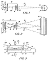
- an electro-optic line printer 11 comprising a multi-gate light valve 12 for exposing a photosensitive recording medium 13 in an image configuration.
- the recording medium 13 is depicted as being a photoconductively coated xerographic drum 14 which is rotated (by means not shown) in the direction of the arrow.
- the recording medium 13 should, therefore, be visualized in the generalized case as being a photosensitive medium which is exposed in an image configuration while advancing in a cross line or line pitch direction relative to the light valve 12.
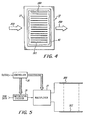
- the light valve 12 includes an electro-optic element 17 and a plurality of individually addressable electrodes 18A-18I.
- the electro-optic element 17 suitably is a y-cut crystal of, say, LiNbO 3 having an optically polishcd reflecting surface 21 which is integral with and disposed between uptically polished input and output faces 22 and 23, respectively.
- the electrodes 18 arc intimately coupled to the electro-optic element 17 adjacent the rcflccting surface 21 and arc distributed across essentially the full width thereof.
- the electrodes 18 arc 1-30 microns wide and are on centers which arc more or less cquidistantly separated to providc a generally uniform interelectrode gap spacing of 1-30 microns.
- the electrodes 18 extend generally parallel to the optical axis of the electro-optic clement 17 and have projections of substantial length along that axis.
- the electrodes 18 could be aligncd at the so-called Bragg angle relative to the optical axis of the electro-optic element 17.
- the electrodes 18 arc aligned parallel to the optical axis of the electro-optic element 17, the light valve 12 will produce a diffraction pattern which is symmetrical about the zero order diffraction component.
- the electrodes 18 are at the Bragg angle relative to the optical axis of the electro-optic clement 17, the light valve 12 will produce an asymmetrical diffraction pattern.
- the input light beam 24A is brought to a wedge-shaped focus (by means not shown) at approximately the centerline of the reflecting surface 21 and is totally internally reflected therefrom to provide an output beam 24B which exits from the electro-optic element 17 through its output face 23.
- the input beam 24A illuminates substantially the full width of the electro-optic element 17, and the output bcam 24B is phase front modulated in accordance with the differentially encoded data samples applied to the electrodes 18A-18I.
- scrial input data samples which represent picture elements for successive lines of an imagc. are applied to a differential encoder 25 at a predetermined data rate.
- the encoder 25 differentially encodes the input samples on a line-by-line basis in response to control signals from a controller 26, and a multiplexer 27 responds to further control signals from the controller 26 to ripple the encoded data samples onto the electrodes 18 at a ripple rate which is matched to the data rate.
- the input data may, of course, be buffered (by means not shown) to match the input data rate to any desired ripple rate. Additionally. the input data may be processed (by means also not shown) upstream of the encoder 25 for text editing. formatting or other purposes, provided that the data samples for the ultimate image arc applied to the encoder 25 in adjacent picture clement sequence.
- each differentially encoded data samplc. other than the first sample for each line of the image has a magnitude whose difference from the previous differentially encoded data sample corresponds to the magnitude of a respective input data sample.
- the first sample for each line of the image is referenced to a common reference potential, such as ground.
- the electrode-to-electrode voltage drops create localized fringe fields 28 within an interaction region 29 of the the electro-optic clcment 17. Furthermore, the fringe fields 28, in turn, cause localized variations in the refractive index of the electro-optic element 17 widthwise of the interaction region 29.
- the refractive index variations within the interaction region 29 faithfully represent the input data samples appearing on the electrodes 18A-18I in differentially encoded form at any given point in time. It therefore follows that the phase front of the light beam 24A (Fig. 3) is sequentially spatially modulated in accordance with the data samples for successive lines of the image as it passes through the interaction region 29 of the electro-optic element 17.
- Schlieren central dark field imaging optics 31 which are optically aligned between the electro-optic element 17 and the recording medium 13 for imaging the modulated light beam 24b onto the recording medium 13.
- the imaging optics 31 convert the spatial phase front modulation of the output bcam 24B into a correspondingly modulated intensity profile and provide any magnification rcquircd to obtain an image of a desired width.
- the illustrated imaging optics 31 include a field lens 34 for focusing the zero order diffraction components 32 of the phase front modulated light beam 2 4B onto a central stop 35 and an imaging lens 36 for imaging the higher order diffraction components onto the recording medium 13, i.e., the image plane for the light valve 12.
- the field lens 34 is optically aligncd between the clcctro-optic element 17 and the stop 35 so that substantially all of the zero order components 32 of the modulated light bcam24B are blocked by the stop 35.
- the higher order diffraction components of the output beam 24B scatter around the stop 35 and are collected by the imaging lens 36 which, in turn, causes them to fall onto the light valve image plane defined by the recording medium 13.
- other p-sensitive readout optics could be used to convert the phase front or polarization modulated light beam provided by the electro-optic element 17 into a light beam having a correspondingly modulatcd intensity profile.
- each neighboring pair of electrodes cooperates with the electro-optic element 17 and with the p-sensitive readout optics 31 to effectively define a local modulator for creating a picture clement at a unique, spatially predetermined position along each line of the image.
- the number of electrodes 18A-18I determines the number of picture elements .that can be printed per line of the image.
- successive lines of the image are printed by sequentially applying successive sets of differentially encoded data samples to the electrodes 18 while the recording medium 13 is advancing in a cross line direction relative to the light valve 12. It should be noted that the differential encoding step may be avoided if ground plane electrodes (not shown) are interposed in alternating paired relationship between the individually addressable electrodes 18.
- the electrodes 18 are advantageously defined by a suitably patterned. electrically conductive layer, generally indicated by 40, which is deposited on an integrated electrical circuit 41, such as a LSI (large scale integrated) silicon circuit, to make electrical contact to the integrated drive electronics42B-42G.
- an integrated electrical circuit 41 such as a LSI (large scale integrated) silicon circuit
- the multiplexer 27 is embodied in the integrated circuit 41, and the electrodes 18A-18I are an extension of the metalised or polysilicon layer 40 which is used to make electrical connections to the output transfer gates or pass transistors 42B - 42G and to the other individual components (not shown) of the multiplexer 27.
- the pass transistors 42B-42G and the other components of the multiplexer 27 are formed on the integrated circuit 41 by using more or less standard LSI component fabrication techniques, and the metalised or polysilicon layer 40 is then deposited on the outer surface 43 of the intcgratcd circuit 41. An etching process or the like is subsequently used to pattern the electrically conductive layer 40 as required to provide electrically independent connections to the electrically independent components of the multiplexer 27 and to form the electrically independent electrodes 18A-18I (only the electrodes 28B-18G can be seen in Fig. 7).
- the data transfer lines 46B-46G for the pass transistors 42B-42G arc defined in the metalised or polysilicon layer 40 by the same etching process which is used to define the electrodes 18.
- the integrated circuit 41 maybe resiliently biased against the reflective surface 21 of the electro-optic element 17, thereby causing the electrodes 18 to generally conform to the contour of the mating surface 21.
- a clamp or similar bonding agent which is schematically represented by the arrows 44 and 45 maintains the electrode bearing surface of the integrated circuit 41 in pressure contact with the reflective surface 21.
- a resilient pressure pad 51 or the like applies a more or less uniform bias to the electrode bearing portion of the integrated circuit 41 so that the integrated circuit 41 flexes as required to cause the electrodes 18 to closely conform to the contour of the reflective surface 21.
- the improved conformance of the electrodes 18 to the mating of reflective surface 21 of the electro-optic element 17 increases the uniformity with which the fringe fields 28 are coupled into the electro-optic element 17, thereby increasing the spatial uniformity of the electro-optic response of the light valve 12.
- the electrodes 18 or the reflective surface 21 of the electro- optic element 17 may be overcoated with a thin dielectric layer (not shown) if the direct contact of the electrodes 18 with the electro-optic element 17 tends to cause unacceptable levels of spurious amplitude and/or phase modulation of the output light beam 24B.
- the pressure pad 51 is disposed between the integrated circuit 41 or a flexible package therefor (not shown) and a rigid base plate 52 so that the pressure pad 51 is compressed under the influence of the clamps 44 and 45.
- the pressure pad 51 underlies the electrode-bearing portion of the integrated circuit 41 and is generally coextensive therewith.
- the restorative forces generated by the compressed pressure pad 51 arc more or less uniformly distributed over the electrode-bearing portion of the integrated circuit 41 to urge or bias that portion of the integrated circuit 41 toward the reflective surface 21 of the electro-optic element 17. Due to its inherent flexibility, the integrated circuit 41 flexes as necessary under the influence of that bias to cause the electrodes 18 to generally conform to the contour of the reflective surface 21.
- the pressure pad 51 is preferably fabricated from a readily deformable elastomer so that it deforms as necessary to accommodate any macroscopic variations in the thickness or flatness of the electro-optic clement 17, the integrated circuit 41, and the base plate 52. Indeed, the integratcd circuit 41 and the base plate 52 arc both shown in Fig. 6 as having exaggerated thickness and flatness variations which arc taken-up by the compressive deformation of the pressure pad 51. If the pressure pad 51 is composed of a relatively incompressible elastomcr, such as silicon rubber, it may be ribbed or otherwise relieved, as at 53 (Fig. 6). to increase its compressibility. Microscopic variations, such as the ordinary surface roughnesses of the electro-optic clement 17 and of the electrodes 18 - have relatively little effect on the deformation of the pressure pad 51 and can be ignored for present purposes.
- the base plate 52 desirably. is an electrically conductive member which is referenced to a suitable ground potential so that a ground return path for the integrated circuit 41 may be completed thereto. If the pressure pad 51 is, say, a silicon rubber or a carbon loaded elastomer which is in electrical contact with both the substrate of the integrated circuit 41 and the base plate 52, the ground return path may be completed through the pressure pad 51. Otherwise, the ground return path may be completed by connecting one or more grounding wires 54 between the substrate of the integrated circuit 41 and the base plate 52.
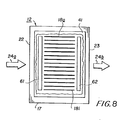
- rails 61 and 62 or similar spacers may be provided for mechanically maintaining the electrodes 18 at a small predetermined nominal gap distance from the electro-optic element 17.
- the rails 61 and 62 are preferably located on opposite sides of the interaction region 29 of the electro-optic element 17 so that the interaction region 29 is free of pressure differentials which might cause undesirable piezoelectric effects.
- the rails 61 and 62 are formed on the electrode-bearing integrated circuit 41 near its lead edge and trail edges, repectively, to engage the electro-optic clement 17 forward and aft, respectively, of the intcracticn region 29.
- the rails 61 and 62 could be formed on the integrated circuit 41 near its front and back edges, repectively, to engage the electro-optic element 17 on opposite lateral sides of the interaction region 29.
- Still another possibility is to form the rails 61 and 62 on the electro-optic clement 17 to engage the electrode substrate 41 either forward and aft or on opposite lateral sides of the electrodes 18.
- the interelectrode gap spacing of the electrodes 18 must be sufficiently large compared to the nominal gap spacing provided by the rails 61 and 62 to ensure that the fringe fields 28 span the gap 63 to penetrate the electro-optic element 17 as previously described.
- the rails 61 and 62 arc each selected to have sufficient height to provide a nominal gap 63 on the order of 0.10 microns.
- increased or decreased interelectrode gap spacings may require or permit a corresponding change in the height of the rails 61 and 62.
- the gap 63 between the electrodes 18 and the electro-optic element 17 advantageously is completely filled with a dielectric material 64 (Fig. 6) having a relative dielectric constant that is significantly greater than 1.
- the dielectric 64 may be a fluid which completely floods the gap 63 and which is confined therein by suitable seals (not shown).
- the dielectric 64 may be a material, such as formvar or methyl methacrylate, which can be loaded into the gap 63 while in a liquid state and then cured in situ into a solid state.
- Still another possibility is to use a finely-divided solid dielectric which is dispersed in a suitable carrier.
- the relative dielectric constant of the dielectric 64 is selected to be as high as possible to minimize the effective electrical thickness of the gap 63, thereby maximizing the coupling efficiency. It should, however, be noted that a marked increase in the coupling efficiency is realized, even if the dielectric 64 has a relative dielectric consatant as low as 3 or 4.
- the gap provided by the rails 61 and 62 (Fig. 8) is a convenient cavity for accommodating the dielectric 64, but a dielectric interface is useful even if there is a relatively irregular gap between the electrodes 18A-18I and the electro-optic element 17.
- a dielectric interface is useful even if there is a relatively irregular gap between the electrodes 18A-18I and the electro-optic element 17.
- one of the advantages of using the dielectric 64 as an interface between the electrodes 18 and the electro-optic clement 17 is that it reduces the effect of any gap irregularities on the relative strcngths of the fringe fields 28 that are coupled into the electro-optic clement 17 through such an irregular gap.
- proximity coupling techniques arc of general applicability to electro-optic devices.
- proximity coupling is particularly relevant to multi-gate light valves and the like which are characterized by having a multitude of electrodes to which separate electrical connections must be made. As will be recalled, it has been shown that such electrical connections may be readily completed through an electrode-supporting LSI circuit
- the present invention provides several solutions to the problcm of avoiding field irregularities in a multigate light valve having proximity coupled electrodes.
- the electrodes can be conformed to the contour of the electro-optic clement of the light valve or can be mechanically spaced from the electro-optic element.
- the mechanically-created gap, or the inherent gap, between the electrodes and the electro-optic element of such a device may be filled with a dielectric having a high relative dielectric constant to improve the coupling efficiency of the device and to further reduce any field irregularities that may be caused by gap irregularities.
Landscapes
- Physics & Mathematics (AREA)
- Nonlinear Science (AREA)
- General Physics & Mathematics (AREA)
- Optics & Photonics (AREA)
- Chemical & Material Sciences (AREA)
- Engineering & Computer Science (AREA)
- Ceramic Engineering (AREA)
- Crystallography & Structural Chemistry (AREA)
- Printers Or Recording Devices Using Electromagnetic And Radiation Means (AREA)
Priority Applications (1)
| Application Number | Priority Date | Filing Date | Title |
|---|---|---|---|
| AT81304272T ATE21457T1 (de) | 1980-09-17 | 1981-09-17 | Elektrooptische vorrichtung. |
Applications Claiming Priority (10)
| Application Number | Priority Date | Filing Date | Title |
|---|---|---|---|
| US06/187,936 US4396252A (en) | 1980-09-17 | 1980-09-17 | Proximity coupled electro-optic devices |
| US187919 | 1980-09-17 | ||
| US06/187,918 US4482215A (en) | 1980-09-17 | 1980-09-17 | Mechanical interface for proximity coupled electro-optic devices |
| US06/187,919 US4370029A (en) | 1980-09-17 | 1980-09-17 | Dielectric interface for proximity coupled electro-optic devices |
| US06/188,171 US4367925A (en) | 1980-09-17 | 1980-09-17 | Integrated electronics for proximity coupled electro-optic devices |
| US194525 | 1980-10-06 | ||
| US06/194,525 US4380373A (en) | 1980-10-06 | 1980-10-06 | Conformable proximity coupled electro-optic devices |
| US187918 | 1988-04-29 | ||
| US188171 | 1994-01-26 | ||
| US187936 | 1998-11-06 |
Publications (2)
| Publication Number | Publication Date |
|---|---|
| EP0051356A1 true EP0051356A1 (de) | 1982-05-12 |
| EP0051356B1 EP0051356B1 (de) | 1986-08-13 |
Family
ID=27539184
Family Applications (1)
| Application Number | Title | Priority Date | Filing Date |
|---|---|---|---|
| EP81304272A Expired EP0051356B1 (de) | 1980-09-17 | 1981-09-17 | Elektrooptische Vorrichtung |
Country Status (4)
| Country | Link |
|---|---|
| EP (1) | EP0051356B1 (de) |
| AU (1) | AU551711B2 (de) |
| BR (1) | BR8105934A (de) |
| DE (1) | DE3175109D1 (de) |
Cited By (3)
| Publication number | Priority date | Publication date | Assignee | Title |
|---|---|---|---|---|
| EP0127362A1 (de) * | 1983-05-26 | 1984-12-05 | Xerox Corporation | Elektroden aus nachgiebigem Material für annäherungsgekoppelte elektrooptische Vorrichtungen |
| EP0062522B1 (de) * | 1981-04-02 | 1985-07-03 | Xerox Corporation | Nah-gekoppelte elektrooptische Vorrichtungen |
| GB2191014A (en) * | 1986-05-28 | 1987-12-02 | Plessey Co Plc | Spatial light modulator |
Citations (5)
| Publication number | Priority date | Publication date | Assignee | Title |
|---|---|---|---|---|
| US3958862A (en) * | 1974-06-14 | 1976-05-25 | Scibor Rylski Marek Tadeusz Vi | Electro-optical modulator |
| FR2316613A1 (fr) * | 1975-07-03 | 1977-01-28 | Battelle Memorial Institute | Dispositif de modulation electro-optique |
| EP0021754A1 (de) * | 1979-06-21 | 1981-01-07 | Xerox Corporation | Elektrooptischer Modulator und seine Verwendung |
| EP0027551A1 (de) * | 1979-10-03 | 1981-04-29 | Rockwell International Corporation | CCD-gesteuerte integrierte optische Modulatoranordnung |
| GB2068577A (en) * | 1980-01-29 | 1981-08-12 | Int Standard Electric Corp | Optical switch |
-
1981
- 1981-09-15 AU AU75254/81A patent/AU551711B2/en not_active Ceased
- 1981-09-16 BR BR8105934A patent/BR8105934A/pt not_active IP Right Cessation
- 1981-09-17 EP EP81304272A patent/EP0051356B1/de not_active Expired
- 1981-09-17 DE DE8181304272T patent/DE3175109D1/de not_active Expired
Patent Citations (5)
| Publication number | Priority date | Publication date | Assignee | Title |
|---|---|---|---|---|
| US3958862A (en) * | 1974-06-14 | 1976-05-25 | Scibor Rylski Marek Tadeusz Vi | Electro-optical modulator |
| FR2316613A1 (fr) * | 1975-07-03 | 1977-01-28 | Battelle Memorial Institute | Dispositif de modulation electro-optique |
| EP0021754A1 (de) * | 1979-06-21 | 1981-01-07 | Xerox Corporation | Elektrooptischer Modulator und seine Verwendung |
| EP0027551A1 (de) * | 1979-10-03 | 1981-04-29 | Rockwell International Corporation | CCD-gesteuerte integrierte optische Modulatoranordnung |
| GB2068577A (en) * | 1980-01-29 | 1981-08-12 | Int Standard Electric Corp | Optical switch |
Non-Patent Citations (2)
| Title |
|---|
| Applied Physics Letters, Vol. 23, No. 4, August 15, 1973, New York, US J.M. HAMMER et al. "Fast Electro-Optic Waveguide Deflector Modulator", pages 176-177. * page 176 * * |
| Journal of Physics D: Applied Physics, Vol. 7, No. 18, 1974, Letchworth-Hertfodshire, GB V. RAMACHANDRAN et al. "Noise Generated in the Total Internal Reflection Electro-Optic Diffraction Deflector/Modulator", pages 2479-2482. * page 2482; figure 1 * * |
Cited By (6)
| Publication number | Priority date | Publication date | Assignee | Title |
|---|---|---|---|---|
| EP0062522B1 (de) * | 1981-04-02 | 1985-07-03 | Xerox Corporation | Nah-gekoppelte elektrooptische Vorrichtungen |
| EP0127362A1 (de) * | 1983-05-26 | 1984-12-05 | Xerox Corporation | Elektroden aus nachgiebigem Material für annäherungsgekoppelte elektrooptische Vorrichtungen |
| US4538883A (en) * | 1983-05-26 | 1985-09-03 | Xerox Corporation | Conformable electrodes for proximity coupled electro-optic devices |
| GB2191014A (en) * | 1986-05-28 | 1987-12-02 | Plessey Co Plc | Spatial light modulator |
| US4867543A (en) * | 1986-05-28 | 1989-09-19 | Plessey Overseas Limited | Spatial light modulator |
| GB2191014B (en) * | 1986-05-28 | 1990-07-04 | Plessey Co Plc | Spatial light modulator |
Also Published As
| Publication number | Publication date |
|---|---|
| AU7525481A (en) | 1982-03-25 |
| AU551711B2 (en) | 1986-05-08 |
| EP0051356B1 (de) | 1986-08-13 |
| BR8105934A (pt) | 1982-06-08 |
| DE3175109D1 (en) | 1986-09-18 |
Similar Documents
| Publication | Publication Date | Title |
|---|---|---|
| EP0062522B1 (de) | Nah-gekoppelte elektrooptische Vorrichtungen | |
| EP0127362B1 (de) | Elektroden aus nachgiebigem Material für annäherungsgekoppelte elektrooptische Vorrichtungen | |
| US4367925A (en) | Integrated electronics for proximity coupled electro-optic devices | |
| JPS6224771B2 (de) | ||
| US4724467A (en) | Light blocking stop for electro-optic line printers | |
| EP0550189B1 (de) | Bildgenerator mit elektrooptischen TIR-Lichtmodulator, der eine Vielzahl von Elektroden pro Bildpunkt aufweist | |
| US4370029A (en) | Dielectric interface for proximity coupled electro-optic devices | |
| EP0087970B1 (de) | Lineare Modulatoren | |
| JPS61239212A (ja) | 電気光学装置のための周辺電界不均一補正 | |
| EP0056334B1 (de) | Elektrooptischer Zeilendrucker in Dünnfilmtechnik | |
| JPS637368B2 (de) | ||
| EP0061926B1 (de) | Mehrweg-Lichtventil für elektrooptische Zeilendrucker mit nicht telezentrischen Abbildungssystemen | |
| EP0057977B1 (de) | Elektrooptischer Zeilendrucker | |
| CA1178326A (en) | Electro-optic line printer | |
| US4380373A (en) | Conformable proximity coupled electro-optic devices | |
| US4437106A (en) | Method and means for reducing illumination nulls in electro-optic line printers | |
| US4993811A (en) | Ridge array light valve device | |
| EP0051356B1 (de) | Elektrooptische Vorrichtung | |
| US4415915A (en) | Multilayer interleaved electrodes for multigate light valves | |
| US4482215A (en) | Mechanical interface for proximity coupled electro-optic devices | |
| EP0072124B1 (de) | Lichtmodulationsvorrichtung mit einem Mehrtor-Lichtventil | |
| EP0048595A1 (de) | Vorrichtung zum zeilenweisen Drucken | |
| JPH0328713B2 (de) | ||
| JPH05216056A (ja) | 液晶光シャッタアレイ素子 | |
| JPH0648330B2 (ja) | 光−光変換素子 |
Legal Events
| Date | Code | Title | Description |
|---|---|---|---|
| PUAI | Public reference made under article 153(3) epc to a published international application that has entered the european phase |
Free format text: ORIGINAL CODE: 0009012 |
|
| AK | Designated contracting states |
Designated state(s): AT BE DE FR GB IT NL |
|
| 17P | Request for examination filed |
Effective date: 19821004 |
|
| GRAA | (expected) grant |
Free format text: ORIGINAL CODE: 0009210 |
|
| AK | Designated contracting states |
Kind code of ref document: B1 Designated state(s): AT BE DE FR GB IT NL |
|
| REF | Corresponds to: |
Ref document number: 21457 Country of ref document: AT Date of ref document: 19860815 Kind code of ref document: T |
|
| REF | Corresponds to: |
Ref document number: 3175109 Country of ref document: DE Date of ref document: 19860918 |
|
| ITF | It: translation for a ep patent filed | ||
| ET | Fr: translation filed | ||
| PLBE | No opposition filed within time limit |
Free format text: ORIGINAL CODE: 0009261 |
|
| STAA | Information on the status of an ep patent application or granted ep patent |
Free format text: STATUS: NO OPPOSITION FILED WITHIN TIME LIMIT |
|
| 26N | No opposition filed | ||
| ITTA | It: last paid annual fee | ||
| PGFP | Annual fee paid to national office [announced via postgrant information from national office to epo] |
Ref country code: BE Payment date: 19980603 Year of fee payment: 18 |
|
| PGFP | Annual fee paid to national office [announced via postgrant information from national office to epo] |
Ref country code: FR Payment date: 19980909 Year of fee payment: 18 Ref country code: AT Payment date: 19980909 Year of fee payment: 18 |
|
| PGFP | Annual fee paid to national office [announced via postgrant information from national office to epo] |
Ref country code: GB Payment date: 19980910 Year of fee payment: 18 |
|
| PGFP | Annual fee paid to national office [announced via postgrant information from national office to epo] |
Ref country code: DE Payment date: 19980925 Year of fee payment: 18 |
|
| PGFP | Annual fee paid to national office [announced via postgrant information from national office to epo] |
Ref country code: NL Payment date: 19980930 Year of fee payment: 18 |
|
| PG25 | Lapsed in a contracting state [announced via postgrant information from national office to epo] |
Ref country code: GB Free format text: LAPSE BECAUSE OF NON-PAYMENT OF DUE FEES Effective date: 19990917 Ref country code: AT Free format text: LAPSE BECAUSE OF NON-PAYMENT OF DUE FEES Effective date: 19990917 |
|
| PG25 | Lapsed in a contracting state [announced via postgrant information from national office to epo] |
Ref country code: BE Free format text: LAPSE BECAUSE OF NON-PAYMENT OF DUE FEES Effective date: 19990930 |
|
| BERE | Be: lapsed |
Owner name: XEROX CORP. Effective date: 19990930 |
|
| PG25 | Lapsed in a contracting state [announced via postgrant information from national office to epo] |
Ref country code: NL Free format text: LAPSE BECAUSE OF NON-PAYMENT OF DUE FEES Effective date: 20000401 |
|
| GBPC | Gb: european patent ceased through non-payment of renewal fee |
Effective date: 19990917 |
|
| PG25 | Lapsed in a contracting state [announced via postgrant information from national office to epo] |
Ref country code: FR Free format text: LAPSE BECAUSE OF NON-PAYMENT OF DUE FEES Effective date: 20000531 |
|
| NLV4 | Nl: lapsed or anulled due to non-payment of the annual fee |
Effective date: 20000401 |
|
| PG25 | Lapsed in a contracting state [announced via postgrant information from national office to epo] |
Ref country code: DE Free format text: LAPSE BECAUSE OF NON-PAYMENT OF DUE FEES Effective date: 20000701 |
|
| REG | Reference to a national code |
Ref country code: FR Ref legal event code: ST |