EP0052643B1 - Umformer mit zwei oder mehreren unabhängig gesteuerten lasten - Google Patents
Umformer mit zwei oder mehreren unabhängig gesteuerten lasten Download PDFInfo
- Publication number
- EP0052643B1 EP0052643B1 EP81901655A EP81901655A EP0052643B1 EP 0052643 B1 EP0052643 B1 EP 0052643B1 EP 81901655 A EP81901655 A EP 81901655A EP 81901655 A EP81901655 A EP 81901655A EP 0052643 B1 EP0052643 B1 EP 0052643B1
- Authority
- EP
- European Patent Office
- Prior art keywords
- circuit
- output
- switch
- controllable
- transfer
- Prior art date
- Legal status (The legal status is an assumption and is not a legal conclusion. Google has not performed a legal analysis and makes no representation as to the accuracy of the status listed.)
- Expired
Links
- 239000003990 capacitor Substances 0.000 claims abstract description 17
- 238000004804 winding Methods 0.000 claims description 66
- 230000004044 response Effects 0.000 claims description 3
- 230000010355 oscillation Effects 0.000 claims description 2
- 239000007787 solid Substances 0.000 claims 4
- 230000008878 coupling Effects 0.000 claims 2
- 238000010168 coupling process Methods 0.000 claims 2
- 238000005859 coupling reaction Methods 0.000 claims 2
- 230000002146 bilateral effect Effects 0.000 claims 1
- 238000010304 firing Methods 0.000 claims 1
- 230000002401 inhibitory effect Effects 0.000 claims 1
- 239000000284 extract Substances 0.000 abstract 1
- 238000000034 method Methods 0.000 description 11
- 230000008569 process Effects 0.000 description 6
- 230000008859 change Effects 0.000 description 5
- 239000000463 material Substances 0.000 description 4
- 238000010586 diagram Methods 0.000 description 3
- 230000004907 flux Effects 0.000 description 3
- 230000000694 effects Effects 0.000 description 2
- 230000003993 interaction Effects 0.000 description 2
- 238000006842 Henry reaction Methods 0.000 description 1
- 230000003247 decreasing effect Effects 0.000 description 1
- 230000001419 dependent effect Effects 0.000 description 1
- 230000002349 favourable effect Effects 0.000 description 1
- 230000006698 induction Effects 0.000 description 1
- 230000004048 modification Effects 0.000 description 1
- 238000012986 modification Methods 0.000 description 1
Images


Classifications
-
- H—ELECTRICITY
- H05—ELECTRIC TECHNIQUES NOT OTHERWISE PROVIDED FOR
- H05G—X-RAY TECHNIQUE
- H05G1/00—X-ray apparatus involving X-ray tubes; Circuits therefor
- H05G1/08—Electrical details
- H05G1/10—Power supply arrangements for feeding the X-ray tube
- H05G1/20—Power supply arrangements for feeding the X-ray tube with high-frequency AC; with pulse trains
-
- H—ELECTRICITY
- H02—GENERATION; CONVERSION OR DISTRIBUTION OF ELECTRIC POWER
- H02M—APPARATUS FOR CONVERSION BETWEEN AC AND AC, BETWEEN AC AND DC, OR BETWEEN DC AND DC, AND FOR USE WITH MAINS OR SIMILAR POWER SUPPLY SYSTEMS; CONVERSION OF DC OR AC INPUT POWER INTO SURGE OUTPUT POWER; CONTROL OR REGULATION THEREOF
- H02M3/00—Conversion of DC power input into DC power output
- H02M3/22—Conversion of DC power input into DC power output with intermediate conversion into AC
- H02M3/24—Conversion of DC power input into DC power output with intermediate conversion into AC by static converters
- H02M3/28—Conversion of DC power input into DC power output with intermediate conversion into AC by static converters using discharge tubes with control electrode or semiconductor devices with control electrode to produce the intermediate AC
- H02M3/305—Conversion of DC power input into DC power output with intermediate conversion into AC by static converters using discharge tubes with control electrode or semiconductor devices with control electrode to produce the intermediate AC using devices of a thyratron or thyristor type requiring extinguishing means
- H02M3/315—Conversion of DC power input into DC power output with intermediate conversion into AC by static converters using discharge tubes with control electrode or semiconductor devices with control electrode to produce the intermediate AC using devices of a thyratron or thyristor type requiring extinguishing means using semiconductor devices only
- H02M3/3155—Conversion of DC power input into DC power output with intermediate conversion into AC by static converters using discharge tubes with control electrode or semiconductor devices with control electrode to produce the intermediate AC using devices of a thyratron or thyristor type requiring extinguishing means using semiconductor devices only with automatic control of the output voltage or current
-
- H—ELECTRICITY
- H02—GENERATION; CONVERSION OR DISTRIBUTION OF ELECTRIC POWER
- H02M—APPARATUS FOR CONVERSION BETWEEN AC AND AC, BETWEEN AC AND DC, OR BETWEEN DC AND DC, AND FOR USE WITH MAINS OR SIMILAR POWER SUPPLY SYSTEMS; CONVERSION OF DC OR AC INPUT POWER INTO SURGE OUTPUT POWER; CONTROL OR REGULATION THEREOF
- H02M7/00—Conversion of AC power input into DC power output; Conversion of DC power input into AC power output
- H02M7/42—Conversion of DC power input into AC power output without possibility of reversal
- H02M7/44—Conversion of DC power input into AC power output without possibility of reversal by static converters
- H02M7/48—Conversion of DC power input into AC power output without possibility of reversal by static converters using discharge tubes with control electrode or semiconductor devices with control electrode
- H02M7/505—Conversion of DC power input into AC power output without possibility of reversal by static converters using discharge tubes with control electrode or semiconductor devices with control electrode using devices of a thyratron or thyristor type requiring extinguishing means
- H02M7/515—Conversion of DC power input into AC power output without possibility of reversal by static converters using discharge tubes with control electrode or semiconductor devices with control electrode using devices of a thyratron or thyristor type requiring extinguishing means using semiconductor devices only
- H02M7/523—Conversion of DC power input into AC power output without possibility of reversal by static converters using discharge tubes with control electrode or semiconductor devices with control electrode using devices of a thyratron or thyristor type requiring extinguishing means using semiconductor devices only with LC-resonance circuit in the main circuit
- H02M7/5233—Conversion of DC power input into AC power output without possibility of reversal by static converters using discharge tubes with control electrode or semiconductor devices with control electrode using devices of a thyratron or thyristor type requiring extinguishing means using semiconductor devices only with LC-resonance circuit in the main circuit the commutation elements being in a push-pull arrangement
- H02M7/5236—Conversion of DC power input into AC power output without possibility of reversal by static converters using discharge tubes with control electrode or semiconductor devices with control electrode using devices of a thyratron or thyristor type requiring extinguishing means using semiconductor devices only with LC-resonance circuit in the main circuit the commutation elements being in a push-pull arrangement in a series push-pull arrangement
Definitions
- This invention relates to power converters, and more particularly, to a series capacitor inverter-converter.
- This type of converter utilizes an internal series resonant circuit which link a source of AC or DC energy with one or more loads simultaneously.
- the above cited type of converter is described in detail in the literature and in the US-A-3,953,779 and US-A-4,096,557.
- the present invention seeks to provide an improved form of converter. Accordingly, the present invention provides a converter circuit for transferring electrical power between circuit input means and first and second circuit output means, comprising:
- controllable resonant circuit switch means means connecting said capacitor means and said inductor means and said controllable resonant circuit switch means for forming series resonant circuit means to transfer electrical power between the circuit input means and the first and second circuit output means through resonant oscillation in said series resonant circuit means; control means connected to said controllable resonant circuit switch means for controlling the transfer of the total electrical power transferred between the circuit input means and the first and second circuit output means;
- first controllable switch means connected for controlling the transfer of electrical power through the first circuit output means
- second controllable switch means connected for controlling the transfer of electrical power through the second circuit output means
- first and second sensing means for sensing the voltage on the first and second output means
- said control means includes includes means coupled to at least said first controllable switch means for controlling transfer of electrical power through the first circuit output means in response to signals received from said first and second sensing means.
- a converter according to the present invention has the capability to supply electrical energy to two or more load simultaneously wherein the said supply of energy can be controlled independently to each load.
- the purpose of this control is to allow each of the load voltages or currents follow an individual reference signal. It employs resonant circuits for the purpose of transfer of energy from a source to two or more loads with each of the loads being controlled independently.
- a favourable electric efficiency of operation is maintained with little or no regard to changes of the voltage of the source of energy within the design limits and to controlled changes of the converter output voltages, within design limits.
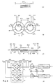
- Fig. 1 is the schematic diagram of a frequency modulated series capacitors inverter-converter governed by a control system for controlling energy exchange between a source of electric energy and plural loads through a series resonant circuit; forms of the physical embodiment will become apparent when reading the material concerning Fig. 1 in the context of the materials concerning the following Figs:
- inductors, capacitors, diodes, controlled rectifiers and resistors are designated by conventional symbols and by reference characters L, C, D, CR and R with various subscripts.
- reference characters for inductors, capacitors, controlled rectifiers and resistors may also be used as algebraic symbols to represent the inductance in Henrys, the capacitance in Farads, and the resistance on Ohms of the several parts. In each case the sense of the usage will be clear from the context.
- the primary part of the power circuit of the frequency modulated series capacitor inverter-converter is exactly the same as in U.S. patent 3,953,779 except for the addition of a second output power transformer XF2, which is located in parallel with output power transformer XF1.
- a primary winding W11 of the transformer XF1 and a primary winding W12 of the transformer XF2 are respectively connected to the primary circuit of the converter.
- Each of the two primary transformer windings W11 and W12 is connected to the point c-b of the resonant circuit individually by way of controllable switches S1 and S2, respectively.
- the primary winding W11 is only connected to the primary converter circuit if switch S1 is closed.
- the transformer XF1 has a secondary winding W21 and is enclosed by a dashed line 1.
- the transformer XF2 has a secondary winding W22 and is enclosed by dashed line 2.
- the first of the indices following the letter W is meant to identify the function of the winding, where the index 1 designates a primary winding and 2 designates a secondary winding.
- the second of the indices of the W is meant to identify the order number of the transformer which corresponds to the single index used after the letters XF. Accordingly the symbol of W21 designates the secondary winding of the power transformer XF1.
- the control system which is presented in the form of a block diagram below the power circuit depicted in Fig. 1 is identical with the control circuit described in U.S. patent 3,953,779 when: only one of the primary windings of the W1i of the transformers XFi is connected to the circuit by way of a single closed switch Si.
- the present control circuit includes plural pulse width modulators shown as PW MODULATOR 1, and PW MODULATOR 2, illustrated within the boxes 17 and 16, respectively.
- both switches S1 and S2 are closed, then both output voltages V o1 and V o2 are applied to attenuators K r1 and k r2 shown in boxes 10 and 11 and in conjunction with the reference sources e r1 and e r2 to provide inputs to comparators 14 and 15 respectively.
- the effect of the output of the comparators 14 and 15 on the Current Control System 5 is such that a current i i in the series resonant circuit is reduced when V oi k ri >e ri and otherwise not affected when v oi k ri ⁇ eri .
- each of the outputs of the comparators 14 or 15 individually will limit the supply of current in the series resonant circuit of the power converter whenever the corresponding output exceeds a voltage vo 1 >e ri /k r1 .
- the control of the series resonant current when multiple output is desired will be explained with reference to the pulse width modulators PW MODULATORS i, (PWMi), 16 and 17 in Fig. 1.
- the PWM1 assumes the function of the switch S1 of Fig. 1 and manifests itself in the form of the signal Si in Fig. 2(b), S1 in this example. If vo 1 k r1 >e r1 , then the pulses S1 will narrow with increasing said inequality. It should be apparent to those skilled in the art that only a fraction of the current i 1 is transferred to the output of the transformer XF1 and the voltage v o1 starts to decay. Decreasing v o1 will reverse the above described process and cause an increase of v o2 .
- a further input to the control system 5 is provided by a current sensor 3 and current to voltage converter and rectifier 4.
- the sensor provides an output in dependence on the current flow through the capacitors C11, C12 and the converter and rectifier 4 integrates this output to provide a signal dependent on the voltage across the capacitors. This signal enables the next alternate conduction of thyristors CR11, CR12 when the voltage across the capacitors is below a predicted level.
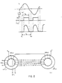
- the transformer XF1 comprises two magnetic cores XF11 and XF12.
- the primary winding W11 encloses both magnetic cores XF11 and XF12.
- the secondary winding W21 encloses only the core XF11.
- An auxiliary winding WS11 encloses core XF11 and continues as winding WS12 to enclose core XF12 and terminates in the open terminals e and f, as shown in Fig. 2(a).
- the two terminals e and f are connected by switch S1, comprising a full wave rectifier bridge including diodes DS1.
- the output of the rectifier bridge is connected to a transistor Q sl which is used to short circuit or open the output terminals of the rectifier bridge.
- the transistor Q s1 is energized by the pulse width modulator PW MODULATOR 1, designated as 17 in Fig. 1.
- the output of PWM1 is indicated as waveform Si in Fig. 2(b). When Si is ON, then Q sl closes. Whenever Si is OFF, then Q sl opens. Switch S1 of Fig. 2(a) is open when signal Si in Fig. 2(b) is OFF and vice versa.
- the -polarity of these windings is such that the magnetic flux energizing winding WS12 transfers energy to the core XF11 to add to the enrgy transferred from winding W11 to winding W21.
- This secondary winding W21 is now fully energized from the primary winding W11, with some of the energy being transferred via the core SF12 as long as switch transistor 0 51 and therefore switch S1 are closed.
- FIG. 2(a) illustrates a transformer SF with an unspecified number of controllable output channels, which is derived by induction from the "switching transformer” illustrated and explained above with reference to Figs. 2(a) and 2(b).
- FIG. 3 A simpler form of independent load control is illustrated in Fig. 3.
- a transformer SFi is connected to a resonant circuit, using the control principle for multiple load operation as explained above with reference to Figs. 1 and 2.
- the switch Si is now embodied by the thyristors CRi1 and CRi2.
- the diodes Di1 and Di2 are used to close the respective circuit.
- a load can also be connected via the above described switches to the resonant circuit without the interposition of a transformer. Any combination of antiparallel controlled bridges or polyphase connections, as described in U.S. Patent 4,096,557, can be used with this configuration.
- FIG. 4(a) through 4(d) Another implementation of control of energy transfer to two loads is illustrated in Figs. 4(a) through 4(d).
- the two cores of the transformers XF1 and SF2 are now simultaneously enclosed by one single primary winding W1.
- the core XF1 is also enclosed by a secondary winding W21.
- the core SF2 is also enclosed by a secondary winding W22. If the magnetic cores are equally loaded by the windings W21 and W22, respectively, then the power entering through winding Wi will be equally distributed to the respective connected loads R L1 and R L2 . If the above described equilibrium of the loads is disturbed, then a modification of the division of power supplied by the winding W1 to the transformer cores becomes necessary in order to maintain the desired voltages on the above said loads R L1 and R L2 .
- the desired division of power transfer through the cores SF1 and SF2 is caused by connection of two auxiliary windings, namely winding WS1 enclosing cores SF1 and winding WS2 enclosing core SF2.
- These windings WS1 and WS2, respectively have taps so that the number of turns around SF1 is larger or smaller than those around SF2, when these two windings WS1 and WS2 are connected to each other by way of a switch.
- the cores SF1 and SF2 have the same cross- section, an assumption which is not requisite for the implementation of the transformer, described with reference to Fig. 4.
- FIG. 4(a) and 4(b) An electric diagram of Fig. 4(c) elucidates the intended windings, cores, and their functional position with respect to each other.
- Fig. 4(d) illustrates the intended use of this transformer. If more power should be diverted to the winding W22 than winding W21, then less turns of the winding WS1 are connected to more turns of the winding WS2 by way of switch S1. This is caused by energizing transistor Q, which closes the above described circuit.
- the transistor Q 1 is energized by an AND gate 25 which requires two inputs. The first input is received from comparator 18 which registers the difference in output of the comparators 14 and 15 of Fig. 1, thus indicating which of the loads is in need of less power.
- the degree of unbalance determined by the PW MODULATOR 1 designated by 17, provides the second input the function of which has been described above with reference to Fig. 2(b).
Landscapes
- Engineering & Computer Science (AREA)
- Power Engineering (AREA)
- Dc-Dc Converters (AREA)
Claims (12)
Priority Applications (1)
| Application Number | Priority Date | Filing Date | Title |
|---|---|---|---|
| AT81901655T ATE42162T1 (de) | 1980-05-21 | 1981-05-20 | Umformer mit zwei oder mehreren unabhaengig gesteuerten lasten. |
Applications Claiming Priority (2)
| Application Number | Priority Date | Filing Date | Title |
|---|---|---|---|
| US06/151,967 US4333135A (en) | 1980-05-21 | 1980-05-21 | Four quadrant AC and DC to AC and DC converter with two or more independently controlled loads |
| US151967 | 1998-09-11 |
Publications (3)
| Publication Number | Publication Date |
|---|---|
| EP0052643A1 EP0052643A1 (de) | 1982-06-02 |
| EP0052643A4 EP0052643A4 (de) | 1983-06-08 |
| EP0052643B1 true EP0052643B1 (de) | 1989-04-12 |
Family
ID=22541021
Family Applications (1)
| Application Number | Title | Priority Date | Filing Date |
|---|---|---|---|
| EP81901655A Expired EP0052643B1 (de) | 1980-05-21 | 1981-05-20 | Umformer mit zwei oder mehreren unabhängig gesteuerten lasten |
Country Status (4)
| Country | Link |
|---|---|
| US (1) | US4333135A (de) |
| EP (1) | EP0052643B1 (de) |
| DE (1) | DE3177030D1 (de) |
| WO (1) | WO1981003400A1 (de) |
Families Citing this family (13)
| Publication number | Priority date | Publication date | Assignee | Title |
|---|---|---|---|---|
| NL8103475A (nl) * | 1981-07-23 | 1983-02-16 | Hollandse Signaalapparaten Bv | Energieomzetter. |
| DE3218535A1 (de) * | 1982-05-17 | 1983-11-17 | Philips Patentverwaltung | Hochspannungserzeuger, insbesondere zur speisung einer roentgenroehre |
| SE456788B (sv) * | 1982-07-12 | 1988-10-31 | Ericsson Telefon Ab L M | Likspaenningsomvandlare foer omvandlingen av en ostabiliserad likspaenning till tre stabiliserade likspaenningar |
| US4663702A (en) * | 1984-10-12 | 1987-05-05 | Kabushiki Kaisha Toshiba | Power converter apparatus and control method thereof |
| US4897775A (en) * | 1986-06-16 | 1990-01-30 | Robert F. Frijouf | Control circuit for resonant converters |
| US4807269A (en) * | 1987-04-02 | 1989-02-21 | Grady John K | Apparatus for powering x-ray tubes |
| NL8702115A (nl) * | 1987-09-07 | 1989-04-03 | Alcatel Nederland | Spanningsomvormer. |
| US5255175A (en) * | 1989-05-15 | 1993-10-19 | Kabushiki Kaisha Toshiba | Power generation system having induction generator and controlled bridge rectifier |
| US5010471A (en) * | 1989-06-26 | 1991-04-23 | Robert F. Frijouf | Three-phase AC-to-AC series resonant power converter with reduced number of switches |
| US5051880A (en) * | 1989-12-29 | 1991-09-24 | At&T Bell Laboratories | Mixed mode regulation controller for a resonant power converter |
| US5270914A (en) * | 1992-01-10 | 1993-12-14 | Lauw Hian K | Series resonant converter control system and method |
| US7746670B2 (en) * | 2006-10-04 | 2010-06-29 | Denso Corporation | Dual-transformer type of DC-to-DC converter |
| JP4546439B2 (ja) * | 2006-10-31 | 2010-09-15 | 株式会社デンソー | 2トランス型dcdcコンバータの磁気回路 |
Family Cites Families (2)
| Publication number | Priority date | Publication date | Assignee | Title |
|---|---|---|---|---|
| US3824441A (en) * | 1973-01-02 | 1974-07-16 | Honeywell Inf Systems | Multivoltage, regulated power supply with fault protection |
| US3953779A (en) * | 1974-05-30 | 1976-04-27 | Francisc Carol Schwarz | Electronic control system for efficient transfer of power through resonant circuits |
-
1980
- 1980-05-21 US US06/151,967 patent/US4333135A/en not_active Expired - Lifetime
-
1981
- 1981-05-20 DE DE8181901655T patent/DE3177030D1/de not_active Expired
- 1981-05-20 WO PCT/US1981/000677 patent/WO1981003400A1/en not_active Ceased
- 1981-05-20 EP EP81901655A patent/EP0052643B1/de not_active Expired
Also Published As
| Publication number | Publication date |
|---|---|
| US4333135A (en) | 1982-06-01 |
| WO1981003400A1 (en) | 1981-11-26 |
| EP0052643A4 (de) | 1983-06-08 |
| DE3177030D1 (en) | 1989-05-18 |
| EP0052643A1 (de) | 1982-06-02 |
Similar Documents
| Publication | Publication Date | Title |
|---|---|---|
| US5381327A (en) | Electrical power inverter | |
| US6014323A (en) | Multiphase power converter | |
| US4333135A (en) | Four quadrant AC and DC to AC and DC converter with two or more independently controlled loads | |
| EP0227382B1 (de) | In einer Leistungsschaltversorgung benutzter Durchflusswandler | |
| KR860006854A (ko) | 안정화 전력 공급 시스템 | |
| US4370607A (en) | Static high voltage switch usable in a switchable high voltage D.C. generator | |
| US4355351A (en) | High repetition rate power pulse generator | |
| US4495555A (en) | Energy converter | |
| US3351841A (en) | Current converter with decoupling network for isolating load from commutation circuit elements | |
| EP0088445B1 (de) | Schaltung zum Übertragen von Energie zu und von Spulen | |
| US4021721A (en) | AC-to-DC converter | |
| US3925715A (en) | Regulated DC to DC converter | |
| US4805078A (en) | Switched power supply for generating a plurality of isolated power voltage for a pulse converter | |
| US3504264A (en) | Variable duty cycle switching apparatus | |
| EP0012648B1 (de) | Einpolige Kommutierungsschaltung | |
| EP0797290B1 (de) | Geregelter Resonanzwandler | |
| US3938026A (en) | Circuit for the simultaneous ignition of a plurality of thyristors | |
| US3815003A (en) | Combined switch and chopper for supplying an a.c. motor | |
| US3422338A (en) | Reversible current converter for selective direction of current flow through d.c. load and including choke coil with unidirectional current flow | |
| CA1171134A (en) | Four quadrant ac and dc to ac and dc converter with two or more independently controlled loads | |
| US3900739A (en) | Device for providing a current supply to inductive loads by use of a battery and a d. c. pulse transformer positioned between battery and load | |
| GB2050083A (en) | Electrical converter | |
| US3733539A (en) | Multi-phase thyristor inverter | |
| SU706911A1 (ru) | Преобразователь посто нного напр жени в переменное | |
| JP2522242B2 (ja) | 交直両用ア−ク溶接電源 |
Legal Events
| Date | Code | Title | Description |
|---|---|---|---|
| PUAI | Public reference made under article 153(3) epc to a published international application that has entered the european phase |
Free format text: ORIGINAL CODE: 0009012 |
|
| AK | Designated contracting states |
Designated state(s): AT CH DE FR GB LI LU NL SE |
|
| 17P | Request for examination filed |
Effective date: 19820121 |
|
| RAP1 | Party data changed (applicant data changed or rights of an application transferred) |
Owner name: FRIJOUF, ROBERT F. Owner name: SCHWARZ, RUTH |
|
| RIN1 | Information on inventor provided before grant (corrected) |
Inventor name: SCHWARZ, FRANCISC C |
|
| GRAA | (expected) grant |
Free format text: ORIGINAL CODE: 0009210 |
|
| AK | Designated contracting states |
Kind code of ref document: B1 Designated state(s): AT CH DE FR GB LI LU NL SE |
|
| PG25 | Lapsed in a contracting state [announced via postgrant information from national office to epo] |
Ref country code: SE Effective date: 19890412 Ref country code: AT Effective date: 19890412 |
|
| REF | Corresponds to: |
Ref document number: 42162 Country of ref document: AT Date of ref document: 19890415 Kind code of ref document: T |
|
| REF | Corresponds to: |
Ref document number: 3177030 Country of ref document: DE Date of ref document: 19890518 |
|
| PG25 | Lapsed in a contracting state [announced via postgrant information from national office to epo] |
Ref country code: LU Free format text: LAPSE BECAUSE OF NON-PAYMENT OF DUE FEES Effective date: 19890531 |
|
| ET | Fr: translation filed | ||
| PLBE | No opposition filed within time limit |
Free format text: ORIGINAL CODE: 0009261 |
|
| STAA | Information on the status of an ep patent application or granted ep patent |
Free format text: STATUS: NO OPPOSITION FILED WITHIN TIME LIMIT |
|
| 26N | No opposition filed | ||
| PGFP | Annual fee paid to national office [announced via postgrant information from national office to epo] |
Ref country code: GB Payment date: 19900518 Year of fee payment: 10 |
|
| PGFP | Annual fee paid to national office [announced via postgrant information from national office to epo] |
Ref country code: FR Payment date: 19900525 Year of fee payment: 10 |
|
| PGFP | Annual fee paid to national office [announced via postgrant information from national office to epo] |
Ref country code: NL Payment date: 19900531 Year of fee payment: 10 |
|
| PGFP | Annual fee paid to national office [announced via postgrant information from national office to epo] |
Ref country code: DE Payment date: 19900629 Year of fee payment: 10 Ref country code: CH Payment date: 19900629 Year of fee payment: 10 |
|
| PGFP | Annual fee paid to national office [announced via postgrant information from national office to epo] |
Ref country code: LU Payment date: 19900717 Year of fee payment: 10 |
|
| PG25 | Lapsed in a contracting state [announced via postgrant information from national office to epo] |
Ref country code: GB Effective date: 19910520 |
|
| PG25 | Lapsed in a contracting state [announced via postgrant information from national office to epo] |
Ref country code: LI Effective date: 19910531 Ref country code: CH Effective date: 19910531 |
|
| PG25 | Lapsed in a contracting state [announced via postgrant information from national office to epo] |
Ref country code: NL Effective date: 19911201 |
|
| GBPC | Gb: european patent ceased through non-payment of renewal fee | ||
| NLV4 | Nl: lapsed or anulled due to non-payment of the annual fee | ||
| PG25 | Lapsed in a contracting state [announced via postgrant information from national office to epo] |
Ref country code: FR Effective date: 19920131 |
|
| REG | Reference to a national code |
Ref country code: CH Ref legal event code: PL |
|
| PG25 | Lapsed in a contracting state [announced via postgrant information from national office to epo] |
Ref country code: DE Effective date: 19920303 |
|
| REG | Reference to a national code |
Ref country code: FR Ref legal event code: ST |