EP0052669A1 - Mémoire à semi-conducteur hautement intégrée et adressage multiple - Google Patents
Mémoire à semi-conducteur hautement intégrée et adressage multiple Download PDFInfo
- Publication number
- EP0052669A1 EP0052669A1 EP80107368A EP80107368A EP0052669A1 EP 0052669 A1 EP0052669 A1 EP 0052669A1 EP 80107368 A EP80107368 A EP 80107368A EP 80107368 A EP80107368 A EP 80107368A EP 0052669 A1 EP0052669 A1 EP 0052669A1
- Authority
- EP
- European Patent Office
- Prior art keywords
- memory
- word
- lines
- addressable
- read
- Prior art date
- Legal status (The legal status is an assumption and is not a legal conclusion. Google has not performed a legal analysis and makes no representation as to the accuracy of the status listed.)
- Granted
Links
- 230000015654 memory Effects 0.000 title claims abstract description 80
- 239000004065 semiconductor Substances 0.000 title claims abstract description 18
- 230000008878 coupling Effects 0.000 claims abstract description 20
- 238000010168 coupling process Methods 0.000 claims abstract description 20
- 238000005859 coupling reaction Methods 0.000 claims abstract description 20
- 238000001465 metallisation Methods 0.000 claims description 7
- 230000008859 change Effects 0.000 claims description 4
- 239000002184 metal Substances 0.000 claims 2
- 239000013256 coordination polymer Substances 0.000 description 9
- 238000005516 engineering process Methods 0.000 description 4
- 239000011159 matrix material Substances 0.000 description 4
- 230000010354 integration Effects 0.000 description 2
- 101100390736 Danio rerio fign gene Proteins 0.000 description 1
- 101100390738 Mus musculus Fign gene Proteins 0.000 description 1
- 230000004913 activation Effects 0.000 description 1
- 230000003321 amplification Effects 0.000 description 1
- 230000008901 benefit Effects 0.000 description 1
- 230000009977 dual effect Effects 0.000 description 1
- 238000003199 nucleic acid amplification method Methods 0.000 description 1
- 238000005457 optimization Methods 0.000 description 1
- 230000008520 organization Effects 0.000 description 1
- 239000007787 solid Substances 0.000 description 1
Images

Classifications
-
- G—PHYSICS
- G11—INFORMATION STORAGE
- G11C—STATIC STORES
- G11C8/00—Arrangements for selecting an address in a digital store
- G11C8/16—Multiple access memory array, e.g. addressing one storage element via at least two independent addressing line groups
Definitions
- the invention relates to a multi-addressable, highly integrated semiconductor memory, the memory cells of which lie in the intersection of word and bit lines and can be controlled via a plurality of independent address systems for parallel reading and / or writing.
- memories which enable two stored words to be read out in parallel or simultaneously to read a certain stored word and to write another word into another memory location.
- a semiconductor memory that allows simultaneous activation of two or more than two-word lines is described in DE-OS 2 327 062.
- this memory has the disadvantage that the words read out are not available at the same time at the output of the memory, but are linked to one another within the memory to form a logical product. It is also not possible to write a word into other memory locations at the same time.
- a storage arrangement is also known from US Pat. No. 3,675,218, in which information can be written into any part, while at the same time information is read out from another, different part of the arrangement.
- IBM-TDB Vol. 19, No. 7, December 1976 describes a memory organization that reads out two-stored words allowed in that coupling elements are assigned to the memory elements, which, however, require a great deal of space in integrated technology.
- a 32 x 9 ECL dual address register is known from IEEE 1977, pages 72 and 73, "International Solid State Circuit Conference", February 16, 1977, which allows two parallel, separate read operations of stored words.
- the technical effort for sensing and selection as well as for registered mail is relatively high and does not allow optimal integration.
- the invention is therefore based on the object of providing a highly integrated semiconductor memory which has at least three accesses, each with independent address decoders, and at least three operations, such as e.g. Reading a word A, reading a word B and writing a word C, as well as being able to carry out any combination of two or individual ones of the three operations in parallel and which avoids the usual memory and register hierarchy in the processors.
- the solution according to the invention consists in that the storage locations consist of at least two storage elements, each Weil are connected via coupling elements with assigned, different bit lines and separate word lines and have at least three independently selectable accesses.
- the coupling elements respond to different polarities of the change in the reference potential of the memory elements and that each such element of a memory location can be controlled separately for reading out via first control and read lines and the other element of the same memory location via second control and read lines and that the write operation for both memory elements of a memory location can be controlled by at least one third access, in that the two memory elements of a memory location are connected to common or coupled write or control lines.
- the double or multiple cell structure has the advantage over the previously known memories that despite the additional accesses a much better and higher integration is achieved.
- the write and read selection via coupling members permits the cells to respond to different polarity of the change of Be 'zugspotentials, reducing the possibility of the separate optimization of the writing and reading speed of the cells is achieved.
- the possibility of expanding the number of read accesses via additional address systems and triple, quadruple, etc. memory cells is technically very easy to implement.
- FIG. 1 A section of a memory matrix, in the intersection of word lines and bit lines, memory cells are arranged and in which two memory cells form a cell pair CP for storing a bit, is shown in FIG. 1.
- This memory has three inputs / outputs (A), (B) and (C), which means that the following memory operations are possible in parallel during operation: Read A, Read B, Write C and any combination of two of the three operations or a single operation thereof.
- Each memory location is formed by a cell pair CP, one cell for reading being assigned to address system A and the other being assigned to address system B. Both memory cells forming the cell pair CP are jointly assigned to address system C, that is, it is written in parallel in this exemplary embodiment, during which the memory accesses (A) and (B) are used for the separate reading of stored information.
- the cell pair CP from two flip-flops is selected only for the present exemplary embodiment. Instead of the two flip-flops, each forming a memory cell, other designs of several memory elements, such as a dynamic single-FET cell, can also be used without further ado. With three memory elements per memory location, three read lines are each coupled to the memory elements via coupling elements.
- each access to the memory has its own address decoder, which can be constructed like the known address decoders. If a register is now queried in the memory according to FIG. 1 via the address decoder (not shown) belonging to the access (A), then only the associated cells of the bit cell pairs CP that belong to the word line associated with the access (A) are selected. are connected. In the present case, these are registers n - 1 (A), n - 2 (A), ). In addition, the vertical bit line outputs labeled (A) become active. However, a word line connected to it (even the same address) connected to it can be selected at the same time via the access (B), the bit line outputs (B) additionally becoming active.
- one word can be written via the access (C), while at the same time one or two other words are read independently via the accesses (A) or (B).
- simultaneous reading and writing of the same line of memory is generally not required.
- the coincidence of the addresses A with C or B with C means nothing other than that the information desired about the accesses A or B is available outside the memory, namely at the access C and is directly available there.
- FIG. 2 shows only one of the two cells of a cell pair CP, the core being formed from a flip-flop known per se.
- a parallel reading of two words is achieved by duplicating the cells of each bit and giving them their own access system (word and read bit lines).
- word and read bit lines there is also only one write access (C) here, ie both cell flip-flops FF of the cell pair shown in FIG. 3 are activated simultaneously via the coupling of the two, which is in principle represented by diodes KWA and KWB Word lines A and B and the common write lines W R (C) are written.
- diodes KWA and KWB Word lines A and B and the common write lines W R (C) are written.
- another word about the (A) or (B) access can be read at the same time.
- a coincidence of the A or B address with a C address must be avoided in the present exemplary embodiment, for example by giving priority to the C address.
- the priority control can either be done logically from the outside or in the memory itself, in which, for example, a C selection switches off the associated A or B selections. Since such circuits are within the scope of the skilled person, a detailed description of such a circuit is not given here.
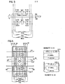
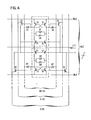
- FIG. 4 A particularly advantageous circuit design that is shown in FIGS. 1 to 3 cells shown in principle is shown in detail in FIG. 4.
- the cross-coupled NPN transistors T3, T 4 and T3 'and T4' can receive Schottky clamping elements in a known manner, which is represented by the Schottky diodes D3 and D4, which accelerate the writing of information into the memory.
- Schottky diodes D1 and D2 or D1 'and D2' are also used as coupling elements to the write bit lines WRC in the exemplary embodiment.
- the transistors T5, T6 or T5 ', T6' are expediently used, because their current amplification produces a stronger read signal.
- the other two bit line pairs R (A) and R (B) are coupled to the cells.
- the word line C corresponds to that in FIG. 3 and is therefore also divided into the lines A and B.
- bit line pairs are in accordance with FIGS. 1 to 4 marked with R (A), R (B) and WR (C) and fully correspond to them.
- the two word lines A and B according to FIG. 3 can also be clearly seen in FIG. 5.
- two sections, namely section Y-y and section X-X are shown on the right. Since these cuts are self-explanatory, a more detailed description is not given.
- Each access (A), (B) and (C) is advantageously assigned a metallization level.
Landscapes
- Engineering & Computer Science (AREA)
- Microelectronics & Electronic Packaging (AREA)
- Static Random-Access Memory (AREA)
Priority Applications (4)
| Application Number | Priority Date | Filing Date | Title |
|---|---|---|---|
| EP80107368A EP0052669B1 (fr) | 1980-11-26 | 1980-11-26 | Mémoire à semi-conducteur hautement intégrée et adressage multiple |
| DE8080107368T DE3070394D1 (en) | 1980-11-26 | 1980-11-26 | Multiple-address highly integrated semi-conductor memory |
| JP56128250A JPS5946079B2 (ja) | 1980-11-26 | 1981-08-18 | 多重アドレス指定可能な記憶装置 |
| US06/317,045 US4412312A (en) | 1980-11-26 | 1981-11-02 | Multiaddressable highly integrated semiconductor storage |
Applications Claiming Priority (1)
| Application Number | Priority Date | Filing Date | Title |
|---|---|---|---|
| EP80107368A EP0052669B1 (fr) | 1980-11-26 | 1980-11-26 | Mémoire à semi-conducteur hautement intégrée et adressage multiple |
Publications (2)
| Publication Number | Publication Date |
|---|---|
| EP0052669A1 true EP0052669A1 (fr) | 1982-06-02 |
| EP0052669B1 EP0052669B1 (fr) | 1985-03-27 |
Family
ID=8186907
Family Applications (1)
| Application Number | Title | Priority Date | Filing Date |
|---|---|---|---|
| EP80107368A Expired EP0052669B1 (fr) | 1980-11-26 | 1980-11-26 | Mémoire à semi-conducteur hautement intégrée et adressage multiple |
Country Status (4)
| Country | Link |
|---|---|
| US (1) | US4412312A (fr) |
| EP (1) | EP0052669B1 (fr) |
| JP (1) | JPS5946079B2 (fr) |
| DE (1) | DE3070394D1 (fr) |
Cited By (3)
| Publication number | Priority date | Publication date | Assignee | Title |
|---|---|---|---|---|
| EP0137318A3 (en) * | 1983-09-07 | 1986-11-12 | Nec Corporation | A semiconductor memory having multiple access |
| EP0149049A3 (fr) * | 1983-12-30 | 1987-01-14 | International Business Machines Corporation | Mémoire de données avec écriture et lecture simultanées |
| EP0288860B1 (fr) * | 1987-04-28 | 1993-10-13 | Advanced Micro Devices, Inc. | Accès rapide pour une mémoire FIFO |
Families Citing this family (8)
| Publication number | Priority date | Publication date | Assignee | Title |
|---|---|---|---|---|
| US4541076A (en) * | 1982-05-13 | 1985-09-10 | Storage Technology Corporation | Dual port CMOS random access memory |
| US4737933A (en) * | 1983-02-22 | 1988-04-12 | Storage Technology Partners | CMOS multiport general purpose register |
| JPS6089895A (ja) * | 1983-10-24 | 1985-05-20 | Matsushita Electric Ind Co Ltd | 半導体記憶装置 |
| US4697251A (en) * | 1985-12-16 | 1987-09-29 | Motorola, Inc. | Bipolar RAM cell |
| US4701882A (en) * | 1985-12-16 | 1987-10-20 | Motorola, Inc. | Bipolar RAM cell |
| US5016214A (en) * | 1987-01-14 | 1991-05-14 | Fairchild Semiconductor Corporation | Memory cell with separate read and write paths and clamping transistors |
| US4817051A (en) * | 1987-07-02 | 1989-03-28 | Fairchild Semiconductor Corporation | Expandable multi-port random access memory |
| US4991138A (en) * | 1989-04-03 | 1991-02-05 | International Business Machines Corporation | High speed memory cell with multiple port capability |
Citations (10)
| Publication number | Priority date | Publication date | Assignee | Title |
|---|---|---|---|---|
| US3651476A (en) * | 1970-04-16 | 1972-03-21 | Ibm | Processor with improved controls for selecting an operand from a local storage unit, an alu output register or both |
| US3737866A (en) * | 1971-07-27 | 1973-06-05 | Data General Corp | Data storage and retrieval system |
| US3968480A (en) * | 1974-04-25 | 1976-07-06 | Honeywell Inc. | Memory cell |
| US3979735A (en) * | 1973-12-13 | 1976-09-07 | Rca Corporation | Information storage circuit |
| US4070657A (en) * | 1977-01-03 | 1978-01-24 | Honeywell Information Systems Inc. | Current mode simultaneous dual-read/single-write memory device |
| FR2357979A1 (fr) * | 1976-07-07 | 1978-02-03 | Gusev Valery | Memoire pour ordinateur |
| US4125877A (en) * | 1976-11-26 | 1978-11-14 | Motorola, Inc. | Dual port random access memory storage cell |
| US4127899A (en) * | 1977-12-05 | 1978-11-28 | International Business Machines Corporation | Self-quenching memory cell |
| US4193127A (en) * | 1979-01-02 | 1980-03-11 | International Business Machines Corporation | Simultaneous read/write cell |
| EP0031488A2 (fr) * | 1979-12-28 | 1981-07-08 | International Business Machines Corporation | Cellule de mémoire et son application dans un système de mémoire utilisant une matrice à accès aléatoire |
Family Cites Families (1)
| Publication number | Priority date | Publication date | Assignee | Title |
|---|---|---|---|---|
| US4280197A (en) * | 1979-12-07 | 1981-07-21 | Ibm Corporation | Multiple access store |
-
1980
- 1980-11-26 EP EP80107368A patent/EP0052669B1/fr not_active Expired
- 1980-11-26 DE DE8080107368T patent/DE3070394D1/de not_active Expired
-
1981
- 1981-08-18 JP JP56128250A patent/JPS5946079B2/ja not_active Expired
- 1981-11-02 US US06/317,045 patent/US4412312A/en not_active Expired - Lifetime
Patent Citations (11)
| Publication number | Priority date | Publication date | Assignee | Title |
|---|---|---|---|---|
| US3651476A (en) * | 1970-04-16 | 1972-03-21 | Ibm | Processor with improved controls for selecting an operand from a local storage unit, an alu output register or both |
| US3737866A (en) * | 1971-07-27 | 1973-06-05 | Data General Corp | Data storage and retrieval system |
| US3979735A (en) * | 1973-12-13 | 1976-09-07 | Rca Corporation | Information storage circuit |
| US3968480A (en) * | 1974-04-25 | 1976-07-06 | Honeywell Inc. | Memory cell |
| FR2357979A1 (fr) * | 1976-07-07 | 1978-02-03 | Gusev Valery | Memoire pour ordinateur |
| US4125877A (en) * | 1976-11-26 | 1978-11-14 | Motorola, Inc. | Dual port random access memory storage cell |
| US4070657A (en) * | 1977-01-03 | 1978-01-24 | Honeywell Information Systems Inc. | Current mode simultaneous dual-read/single-write memory device |
| US4127899A (en) * | 1977-12-05 | 1978-11-28 | International Business Machines Corporation | Self-quenching memory cell |
| US4193127A (en) * | 1979-01-02 | 1980-03-11 | International Business Machines Corporation | Simultaneous read/write cell |
| EP0012796A2 (fr) * | 1979-01-02 | 1980-07-09 | International Business Machines Corporation | Dispositif de mémoire avec cellules pouvant être adressées simultanément pour l'écriture et la lecture d'information |
| EP0031488A2 (fr) * | 1979-12-28 | 1981-07-08 | International Business Machines Corporation | Cellule de mémoire et son application dans un système de mémoire utilisant une matrice à accès aléatoire |
Non-Patent Citations (8)
| Title |
|---|
| 1977 IEEE International Solid-State Circuits Conference, 16. Februar 1977, seiten 72-73 New York, U.S.A. J.R. REINERT et al.: "A 32 X 9 ECL Dual Address Register Using an Interleaving Cell Technique" * |
| IBM Technical Disclosure Bulletin, Band 22, Nr. 10, Marz 1980, seiten 4553-4554 Armonk, U.S.A. R.T. DENNISON et al.: "Multi-Port Array Cell" * seite 4553, zeile 1 - seite 4554, zeile 7; figuren * * |
| IBM Technical Disclosure Bulletin, Band 22, Nr. 4, September 1979, seiten 1489-1492 Armonk, U.S.A. E.J. CRETELLI et al.: "Dual Schottky Diode Cell" * |
| IBM Technical Disclosure Bulletin, Band 23, Nr. 1, Juni 1980, seiten 180-186 Armonk, U.S.A. J.R. CAVALIERE et al.: "Memory Cell Adapted for Different Combinations of Simultaneous Read and Write Operations" * |
| IBM Technical Disclosure Bulletin, Band 23, Nr. 2, Juli 1980, seiten 657-658 Armonk, U.S.A. C.A. PRICE: "Simultaneous Access Memory" * seite 657, zeile 1 -seite 658, zeile 19; figuren 1, 2 * * |
| IEEE Transactions on Computers, Band C-29, Nr. 8, August 1980, seiten 689-694 New York, U.S.A. S.S.L. CHANG: "Multiple-Read Single-Write Memory and its Applications" * |
| Proceedings of the Fall Joint Computer Conference, Band 29, 7. - 10. November 1966, AFIPS seiten 315-331 San Francisco, U.S.A. I. CATT et al.: "A High-Speed Integrated Circuit Scratchpad Memory" * figur 1 * * |
| Proceedings of the IFAC/IFIP Symposium, 21. - 23. Oktober 1965, seiten 259-273 Munchen, DE. H. STOPPER et al.: "Eine Integrierte Schaltung zur Realisiering Eines Halbleiterspeichers" * seiten 270-272, Abschnitt: "Die Integrierte Schaltung"; figuren 7, 10 * * |
Cited By (3)
| Publication number | Priority date | Publication date | Assignee | Title |
|---|---|---|---|---|
| EP0137318A3 (en) * | 1983-09-07 | 1986-11-12 | Nec Corporation | A semiconductor memory having multiple access |
| EP0149049A3 (fr) * | 1983-12-30 | 1987-01-14 | International Business Machines Corporation | Mémoire de données avec écriture et lecture simultanées |
| EP0288860B1 (fr) * | 1987-04-28 | 1993-10-13 | Advanced Micro Devices, Inc. | Accès rapide pour une mémoire FIFO |
Also Published As
| Publication number | Publication date |
|---|---|
| DE3070394D1 (en) | 1985-05-02 |
| US4412312A (en) | 1983-10-25 |
| EP0052669B1 (fr) | 1985-03-27 |
| JPS5946079B2 (ja) | 1984-11-10 |
| JPS5798189A (en) | 1982-06-18 |
Similar Documents
| Publication | Publication Date | Title |
|---|---|---|
| DE2822219C2 (de) | Auf einem Chip integrierte Logikschaltungen | |
| DE2723821C2 (de) | Programmierbare logische Anordnung | |
| DE4128919C2 (de) | Halbleiterspeichereinrichtung und Verfahren zum Betrieb derselben | |
| DE3851099T2 (de) | Erweiterbarer Schreib- und Lesespeicher mit Vielfach-Ein-Ausgabe-Einheit. | |
| EP0012796B1 (fr) | Dispositif de mémoire avec cellules pouvant être adressées simultanément pour l'écriture et la lecture d'information | |
| DE2059917C3 (de) | Hybridadressierter Datenspeicher | |
| DE2062211A1 (de) | Speicheranordnung mit gleichzeitigem Zugriff auf n Speicherstellen | |
| DE10214749A1 (de) | Inhaltsadressierbare Speicherzelle | |
| DE4238062C2 (de) | Multiport-Speichereinrichtung | |
| EP0052669B1 (fr) | Mémoire à semi-conducteur hautement intégrée et adressage multiple | |
| DE2450528A1 (de) | Speichergesteuerte signalverteilungseinrichtung | |
| DE2925925C2 (de) | Informationsspeicher | |
| DE3886938T2 (de) | Reprogrammierbare logische Sicherung für logische Anordnungen, basierend auf einer 6-Elementen-SRAM-Zelle. | |
| EP0162934B1 (fr) | Mémoire semi-conductrice | |
| DE1524898C3 (de) | Datenspeicher mit direktem mehrdimensionalen Zugriff zur gleichzeitigen Entnahme mehrerer Wörter | |
| DE1499202A1 (de) | Einrichtung zum Adressieren von Speicherbereichen | |
| DE69322436T2 (de) | Halbleiterspeicheranordnung | |
| EP0224887B1 (fr) | Matrice de portes en technologie CMOS | |
| DE68922738T2 (de) | Hochintegrierter Halbleiterspeicher mit Mehrfachzugang. | |
| DE2022256C2 (de) | Festwertspeicher- und Decoderanordnung | |
| DE3430734C2 (fr) | ||
| DE1295656B (de) | Assoziativer Speicher | |
| DE2152706B2 (de) | Monolithischer integrierter halbleiterspeicher fuer binaere daten | |
| DE60023213T2 (de) | RAM Speicher | |
| DE3121562A1 (de) | Programmierbare logische hochintegrierte schaltungsanordnung |
Legal Events
| Date | Code | Title | Description |
|---|---|---|---|
| PUAI | Public reference made under article 153(3) epc to a published international application that has entered the european phase |
Free format text: ORIGINAL CODE: 0009012 |
|
| 17P | Request for examination filed |
Effective date: 19810828 |
|
| AK | Designated contracting states |
Designated state(s): CH DE FR GB IT NL |
|
| ITF | It: translation for a ep patent filed | ||
| GRAA | (expected) grant |
Free format text: ORIGINAL CODE: 0009210 |
|
| AK | Designated contracting states |
Designated state(s): CH DE FR GB IT LI NL |
|
| REF | Corresponds to: |
Ref document number: 3070394 Country of ref document: DE Date of ref document: 19850502 |
|
| ET | Fr: translation filed | ||
| PG25 | Lapsed in a contracting state [announced via postgrant information from national office to epo] |
Ref country code: LI Effective date: 19851130 Ref country code: CH Effective date: 19851130 |
|
| PLBE | No opposition filed within time limit |
Free format text: ORIGINAL CODE: 0009261 |
|
| STAA | Information on the status of an ep patent application or granted ep patent |
Free format text: STATUS: NO OPPOSITION FILED WITHIN TIME LIMIT |
|
| 26N | No opposition filed | ||
| REG | Reference to a national code |
Ref country code: CH Ref legal event code: PL |
|
| PGFP | Annual fee paid to national office [announced via postgrant information from national office to epo] |
Ref country code: DE Payment date: 19901124 Year of fee payment: 11 |
|
| ITTA | It: last paid annual fee | ||
| PGFP | Annual fee paid to national office [announced via postgrant information from national office to epo] |
Ref country code: FR Payment date: 19911028 Year of fee payment: 12 |
|
| PGFP | Annual fee paid to national office [announced via postgrant information from national office to epo] |
Ref country code: GB Payment date: 19911104 Year of fee payment: 12 |
|
| PGFP | Annual fee paid to national office [announced via postgrant information from national office to epo] |
Ref country code: NL Payment date: 19911130 Year of fee payment: 12 |
|
| PG25 | Lapsed in a contracting state [announced via postgrant information from national office to epo] |
Ref country code: DE Effective date: 19920801 |
|
| PG25 | Lapsed in a contracting state [announced via postgrant information from national office to epo] |
Ref country code: GB Effective date: 19921126 |
|
| PG25 | Lapsed in a contracting state [announced via postgrant information from national office to epo] |
Ref country code: NL Effective date: 19930601 |
|
| NLV4 | Nl: lapsed or anulled due to non-payment of the annual fee | ||
| GBPC | Gb: european patent ceased through non-payment of renewal fee |
Effective date: 19921126 |
|
| PG25 | Lapsed in a contracting state [announced via postgrant information from national office to epo] |
Ref country code: FR Effective date: 19930730 |
|
| REG | Reference to a national code |
Ref country code: FR Ref legal event code: ST |