EP0052671A1 - Automatischer Simulator für Flugzeugfunknavigationssignale - Google Patents
Automatischer Simulator für Flugzeugfunknavigationssignale Download PDFInfo
- Publication number
- EP0052671A1 EP0052671A1 EP19800201100 EP80201100A EP0052671A1 EP 0052671 A1 EP0052671 A1 EP 0052671A1 EP 19800201100 EP19800201100 EP 19800201100 EP 80201100 A EP80201100 A EP 80201100A EP 0052671 A1 EP0052671 A1 EP 0052671A1
- Authority
- EP
- European Patent Office
- Prior art keywords
- signal
- rate
- value
- register
- stored
- Prior art date
- Legal status (The legal status is an assumption and is not a legal conclusion. Google has not performed a legal analysis and makes no representation as to the accuracy of the status listed.)
- Granted
Links
- 230000003213 activating effect Effects 0.000 claims abstract description 4
- 239000003550 marker Substances 0.000 claims description 30
- 230000004044 response Effects 0.000 claims description 14
- 238000013459 approach Methods 0.000 claims description 4
- 230000008878 coupling Effects 0.000 claims 7
- 238000010168 coupling process Methods 0.000 claims 7
- 238000005859 coupling reaction Methods 0.000 claims 7
- 230000000717 retained effect Effects 0.000 claims 5
- 238000012360 testing method Methods 0.000 abstract description 8
- 238000004088 simulation Methods 0.000 abstract description 4
- 102100023941 G-protein-signaling modulator 2 Human genes 0.000 description 33
- 101000904754 Homo sapiens G-protein-signaling modulator 2 Proteins 0.000 description 33
- 238000010586 diagram Methods 0.000 description 14
- 238000012986 modification Methods 0.000 description 11
- 230000004048 modification Effects 0.000 description 11
- 239000000872 buffer Substances 0.000 description 10
- 238000012546 transfer Methods 0.000 description 8
- 239000013078 crystal Substances 0.000 description 7
- 238000000034 method Methods 0.000 description 6
- 230000008569 process Effects 0.000 description 5
- 230000007704 transition Effects 0.000 description 3
- 239000002131 composite material Substances 0.000 description 2
- 238000013461 design Methods 0.000 description 2
- 235000008331 Pinus X rigitaeda Nutrition 0.000 description 1
- 235000011613 Pinus brutia Nutrition 0.000 description 1
- 241000018646 Pinus brutia Species 0.000 description 1
- 230000002411 adverse Effects 0.000 description 1
- 230000008859 change Effects 0.000 description 1
- 238000004891 communication Methods 0.000 description 1
- 238000012937 correction Methods 0.000 description 1
- 229910044991 metal oxide Inorganic materials 0.000 description 1
- 150000004706 metal oxides Chemical class 0.000 description 1
- 230000010355 oscillation Effects 0.000 description 1
- 238000011160 research Methods 0.000 description 1
- 230000000638 stimulation Effects 0.000 description 1
- 238000012956 testing procedure Methods 0.000 description 1
Images






Classifications
-
- G—PHYSICS
- G01—MEASURING; TESTING
- G01S—RADIO DIRECTION-FINDING; RADIO NAVIGATION; DETERMINING DISTANCE OR VELOCITY BY USE OF RADIO WAVES; LOCATING OR PRESENCE-DETECTING BY USE OF THE REFLECTION OR RERADIATION OF RADIO WAVES; ANALOGOUS ARRANGEMENTS USING OTHER WAVES
- G01S1/00—Beacons or beacon systems transmitting signals having a characteristic or characteristics capable of being detected by non-directional receivers and defining directions, positions, or position lines fixed relatively to the beacon transmitters; Receivers co-operating therewith
- G01S1/02—Beacons or beacon systems transmitting signals having a characteristic or characteristics capable of being detected by non-directional receivers and defining directions, positions, or position lines fixed relatively to the beacon transmitters; Receivers co-operating therewith using radio waves
- G01S1/022—Means for monitoring or calibrating
- G01S1/028—Simulation means, e.g. of beacon signals therefor
Definitions
- the present invention pertains to the automatic signal simulator art and, more particularly, to a fully automated aircraft radio navigation simulation system.
- VOR very high frequency, omni- directional
- the VOR signal is comprised of a carrier selected between 108 and 116.5 megahertz modulated with 30 hertz and 9.96 kilohertz signals.
- the VOR signal is radiated in all directions from the transmitter site, with each radial radiated line containing a predetermined phasing of the two tones.
- an aircraft in receiving the VOR signal can determine its position relative to the transmitting site by detecting the relative phasing of the tones on the carrierd and using a "lookup" table to determine the relative position indicated by that tone phasing.
- a marker beacon is a tone of selected frequency which modulates a 75 megahertz carrier. The frequency of the tone indicates to the aircraft the distance of the aircraft from a given geographical point. Thus, a 400 hertz tone might be used to indicate that the aircraft is two miles from a city, a 1300 hertz tone that it is one mile from the city, and so forth.
- the localizer signal is generally comprised of a carrier selected between 108.1 and 111.9 megahertz which is modulated by 90 and 150 hertz tones.
- the localizer signal is radiated from the ground site such that if the aircraft is to the right of a desired flight path it receives a higher proportion of the 150 hertz tone and if it is off to the left it receives a higher proportion of the 90 hertz tone.
- the sum of the amplitudes of the two tones always remains a constant, with the proportion determining the left/right relative position of the aircraft with respect to the runway center line.
- the glideslope signal is comprised of a carrier selected between 327 and 337 megahertz, also modulated by 90 and 150 hertz tones.
- the sum of the amplitudes of the two tones is always a constant.
- the:relative proportion of each tone to the sum of the two is indicative of the vertical glide path of the aircraft with respect to a desired vertical glide path.
- Signals of 90 hertz, and 150 hertz, each at a fixed level are applied to opposite ends of the potentiometers .
- the two signals may be combined in any desired proportion, with the amplitude of the sum of the two signals always being a constant.
- apparatus which automatically simulates the glideslope, localizer andvery high frequency, omni-directional (VOR) guidance signals normally received by an aircraft.
- the apparatus includes a computer control which is programable to produce digital signals representative of: a) a desired final glideslope value and the rate at which said final glideslope value should be approached, b) a desired final localizer value and the rate at which said final localizer value should be approached, and c) a desired final VOR value and the rate at which said final VOR value should be approached.
- Glideslope circuitry includes means to receive digital signals representative of the glideslope final value and of the rate at which the final value should be approached and further means which respond to the received signals to generate the desired final value at the desired rate.
- Localizer circuitry includes means to receive the digital signals representative of the final localizer value and of the rate at which the final localizer value should be approached and further means responsive to the received signals to generate the desired final value at the desired rate.
- VOR circuitry includes means to receive the digital signals representative of the final VOR value and the rate at which the final VOR value should be approached.
- the computer control communicates to the glideslope circuitry, localizer circuitry and VOR circuitry on a common bus.
- Each of the various circuitry is assigned a predetermined address which the computer uses to route desired final values and rates to each of the circuits.
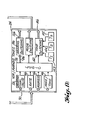
- FIGURE 1 is a block diagram illustrating the topology of the preferred embodiment of the invention.
- a computer 10 in accordance with its programing, creates signals on its output bus 12 which, when coupled to the remaining portions of the system, results in the generation of particular signals at desired rates.
- computer 10 is comprised of a commercially available Hewlett Packard type 9845 computer.
- the output bus 12 for the type 9845 computer is comprised of sixteen lines, eight containing data and eight of control.
- the programing of computer 10 would be well known to anyone of ordinary skill in this art.
- computer 10 could be appropriately programed such that the various signals generated precisely simulate the signals encountered by an aircraft in flight.
- the computer is capable of activating the various signals, at a prescribed rate to simulate any desired set of conditions which an aircraft might actually experience.
- Interface 14 which is preferably a commercially available Fairchild Model 4880 interface unit, decodes the data lines on bus 12 into 40 output lines on its output bus 16.
- the 40 line output bus 16 is fed in parallel to each of three circuits including a localizer circuit 20, a glideslope circuit 22 and a very high frequency, omnidirectional (VOR)/marker tone circuit 24.
- the bus 16 is shown feeding to connectors 26, 28 and 30 of the respective boards 20,22 and 24.
- Each of the circuits 20, 22 and 24 shares in common the fact that each includes an address register 32, 34 and 36, rate registers 42, 44 and 46 and final value registers 52, 54 and 56, respectively.
- Each of these components within any one circuitry block connect to the same lines of the bus 16.
- the address registers 32,34 and 36 in the preferred embodiment of the invention, all connect to lines 3-6 of the 40 line bus 16.
- the rate registers 42, 44 and 46 all connect to lines 11-18 of the 40 line bus 16 and, the final value registers 52,54 and 56 all connect to lines.19-30 of the 40 line bus, with the VOR/marker tone circuit tone also being connected to lines 31 and 32.
- the computer 10 accesses a particular one of the circuits 21, 22 and 24 by outputting an appropriate address on output..bus 12 which, correspondingly, becomes a predetermined sequence on lines 3-6 of bus 16. Thus, if the computer wishes to access localizer circuit 20 it might produce a signal which, on lines 3-6 of bus 16 is 0001.
- the address of the glideslope circuit 22 may be assigned 0010 and that of the VOR/marker tone circuit 24 as 0101. Unless one of the circuitry blocks receives its address, it will not respond to further commands from the computer.
- the localizer circuit 20 which is more fully described herein below with respect to FIGURE 3, operates as follows. Upon receiving an appropriate address at its address register 32, the localizer circuit 20 enters into its logic circuit 62 both the final value from its final value register 52 and the rate at which the final value should be approached from its rate register 42. Contained within the logic circuit 62 is the previous localizer value and, as such, the localizer 62 digitally increments from its previous value to the final value, as determined by final value register 52, at the rate determined by the rate register 42. In the process of incrementing from the initial value to the final value the logic circuit 62 goes through a digital transition which, via a conventional digital to analog circuit 72, results in a corresponding analog signal at the converter's output 82.
- This control signal from the converter's output 82 is fed to the control input of a combiner circuit 92. Also fed to combiner circuit 92 is a 90 hertz tone, here represented as originating from block 102 and a 150 hertz tone originating from block 112. Each of the two tones is at some predetermined level.
- the combiner circuit in response to the signal at its control input on line 82, combines the 90 hertz and 150 hertz tones in predetermined proportions such that the sum of the amplitudes of the two tones is always constant.
- This combined signal which is seen to be the information on the conventional localizer signal, is produced at an output 122 which is fed via a line 123 to the first input 131 of a generator 130.
- the glideslope circuit 22 operates identically to the localizer circuit 20 such that when it receives its proper address on address register 34 its logic circuitry 64 responds by digitally incrementing from its present to the final value, as determined by final value register 54 at the rate determined by rate register 44.
- the digital transitions at logic circuitry 64 output are monitored by the digital analog converter 74 producing a corresponding analog signal at the converter's output 84.
- This output is applied to the control input of a combiner circuit 94 which combines a 90 hertz tone, originating from block 104, and a 150 hertz tone, originating from a block 114, into a resultant output signal at its output 124.
- the combined signal is in turn fed via a line 125 to the second input 132 of the generator 130.
- VOR/marker tone circuit block 24 Operation of the VOR/marker tone circuit block 24 may be understood as follows. Upon its address register 36 receiving an appropriate address, a .logic circuit 76, which contains the present value of the VOR signal in digital form, is caused to increment from the present value to the final value, a determined by register 56, at the rate determined by rate register 46. The instantaneous digitial transitions corresponding to the desired VOR signal experienced by logic circuit 76 appear on its output bus 86 and are fed to the input of bearing switching circuitry 96 as will be better understood herein below with respect to FIGURE 5. Bearing switching circuitry 96 activates selected switches in response to the signal on line 86 thereby producing at its output 126 a switching sequence which, when fed via a bus 127 to the third input 133 of generator 130 causes generator 130 to produce a desired VOR signal.
- circuitry 24 is capable of creating any one of several beacon marker tones.
- address 36 receives an address corresponding to a desired marker tone
- logic circuit 76 processes a digital signal corresponding to that tone via a mode/tone register 140. This results in tone switching circuitry 142 to be activated.
- Fed into tone switching circuitry 42 are.three distinct tones, originating from blocks 143-145, corresponding to the beacon tones to be used.
- the tone switching circuit in response to the logic 76, feeds the selected one of the three tones 143-145 to an output line 146 which in turn feeds through bus 127 to the generator 130.
- generator 130 is comprised of a commercially available NAV 401 L generator, available from Instrument Flight Research. As supplied, generator 130-is capable of generating any of the above discussed signals in response to mechanical switches on the generators front panel. Thus, for example, a series of thumbwheel switches are setable between 0 and 360° which, when set, result in the generation of a corresponding VOR signal.
- the generator 130 is supplied with potentiometers corresponding to the localizer and glideslope signals. At either ends of the potentiometers are fed the fixed level 90 and 150 hertz tones.
- the tap of the potentiometer contains a constant amplitude signal which is the sum of the two tones in any desired proportion depending upon the position of the tap with respect to the end points.
- the circuitry of the generator 130 is modified such that the computer 10 has complete control over all of the signals to be generated by generator 130.
- the 90 and 150 hertz tones as shown in blocks 102, 112, 104 and 114 are internally generated within generator 130 as are the beacon tones 143-145.
- the modified generator 130 in response to signals at its inputs 131-133, the modified generator 130 produces at its antenna output 150 the desired set of simulated radio navigation signals which may then be radiated to test a given aircraft system.
- arrows extending from a line indicate connections to external circuitry and not necessarily the direction of current flow.
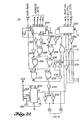
- FIGURES 2A, B and C are detailed schematic diagrams of the localizer circuit 20 shown in FIGURE 1.
- the address bits, carried on lines 3-6 of the 40 line bus 16 of FIGURE 1 are applied to pins 12-15 of an integrated circuit 200.
- Integrated circuit 200 is a one of ten decoder, commercially available as a TTL part 7442.
- a binary address on the input pins 12-15 is converted to its decimal equivalent in decoder 200 causing a corresponding decimal one of 10 output pins to be driven to a low state.
- the address of the localizer is 0001, corresponding to the decimal number 1.
- pin 2 of decoder 200 is driven to its low state.
- OR gate 204 This is coupled through switch 1 to inverter 202 which inverts the low to a high state at pin'l of OR gate 204.
- the other input to OR gate 204 at pin 2 is low since the decimal 8 place, at pin 10 of decoder 200 is high and thereafter inverted by inverter 206 to a low state.
- the output at pin 3 of OR gate 204 is high being fed. to one input at pin 5 of the OR gate 208.
- OR gates 204 and 208 are both provided in a type 7432 integrated circuit.
- the remaining input at pin 4 of OR gate 208 is low due to the inversion of inverter 210 at the pin 1 output from decoder 200.
- the output, at pin 6 of OR gate 208 is driven high and is coupled to pin 9 of AND gate 212.
- Coupled to the second input at pin 10 of AND gate 212 is a transfer pulse which appears on line 33 of the bus 16.
- the transfer pulse is generated by the computer approximately ten microseconds after data is presented on the bus line. This allows the data to settle before it is entered into circuitry in response to the transfer pulse.
- a transfer pulse'AND gate 212 produces a pulsed high at its output at pin 8.
- the pulsed high is inverted by inverter 214 to a low level and then inverted again by paralleled inverters 216 and 218 to a high level.
- the purpose of inverters 216 and 218 is to provide high drive fanout capability.
- OR gate 220 The pulsed high output from inverters 216,218 is applied to one input at pin 1 of OR gate 220.
- the signal at the remaining input at pin 2 of OR gate 220 is at a low level as is understood as follows.
- the outputs at pins 3 and 11 of decoder 200 are high which invert to lows through inverters 222 and 224 at the inputs of pins 9 and 10 of OR gate 226.
- the output at pin 8 of OR gate 226 is low resulting in a low at the input of pin 12 of OR gate 228. This low, coupled with the low at its remaining input at pin 13, results in a low at its output at pin 11.
- OR gates 204, 208,226 and 228 are all provided on a 7432 integrated circuit.
- OR gate 228 is coupled to pin 12 of AND-gate 230 which, along with the low level at its second input level at pin 13 results in a low level at its output at pin 11. This is subsequently inverted by an inverter 232 and fed via further parallel connected inverters 234 and 236 to an output point A.
- Storage register 240 which is comprised of a type 74L95 integrated circuit, is operable in either a serial or parallel load mode. In this case, the parallel load mode is desired and thus pin 6 of the integrated circuit is biased high via a parallel array of inverters 242-245.
- data on lines 8,9 and 10 from the 40 line bus 16 is transferred to output pins 10,12 and 13, respectively of register 240 upon receipt of the transfer pulse at its pin 8.
- line 10 of the 40 line bus 16 is high causing pin 13 of register 240 to be nigh.
- the pulsed high out of inverters 216,218 is further coupled to the number 8 pins of registers 380-284.
- the pin 6 of each of the registers 280-284 is driven high via inverters 242-245 thus causing each of these type 74L95 registers to operate in the parallel mode.
- the inputs to registers 280 and 281 receive the localizer rate control bits appearing on lines 11-18 of bus 16.
- each of the registers 280,281 parallel loads the data bits at its inputs to the divisor inputs of a pair of type 7497 divider IC's 290,291.
- loaded into the first divider 290 is a binary number corresponding to a first desired divisor N .
- loaded into the second divider 29 1 is a second divisor N 2 .
- Applied to the input at pin 9 of the first divider 290 is a 500 hertz waveform generated by a type 555 multi- - vibrator IC 292. As is well known with this IC, external components 293, 294 and 295 are selected to produce a.500 hertz waveform at its output at pin 3.
- the 500 hertz waveform appearing at the input at pin 9 of the first divider 290 is divided by the first divisor N 1 and outputted at its output at pin 5.
- This divided signal is in turn applied to the input of pin 9 of the second divider 291.
- the signal is divided by the divisor N 2 and appears at the output pin 6 of the divider.
- AND gated 300,302 along with AND gate 212,230 are comprised of type 7408 integrated circuits.
- the remaining inputs at pins 1 and 4 of AND gated 300,302 are determined by the outputs at pins 12 and 13 of a comparator chain comprised of comparator type 74L85 integrated circuits 310-312.
- the comparators 310-312 are wired, as shown, to compare the number loaded into registers 282-284 to the present count of the binary counters 320-322.
- the numbers appearing in the registers 282-284 are the desired final value of the localizer signal as appearing on lines 19-30 of the 40 line bus 16.
- the numbers contained within counters 320-322 correspond to the present value of the localizer signal.
- the computer is programed to change the localizer signal, it loads the desired final value into the registers 282-284.
- the comparators 310-312 compare the desired new value to the present value as determined by counters 320-322 and, should the desired value exceed the present value the output at pin 13 of comparator 312 is raised to a high level whereas, if the desired new value is less than the present value, the output of pin 12 of comparator 312 is activated to a high state.
- AND gate 300 transmits the 500 hertz/N signal through an inverter 330 to the count up input at pin 5 of counter 320.
- Counter 320 increments up with the carry appearing at its output pin 12 being routed to the carry input of counter 321.
- the carry output of counter 321 is loaded to the carry input of counter 322. In this manner, the counters 320-322 will count up at the rate determined by the divisor N to the value called for by the computer.
- AND gate 302 routes the 500 hertz/N signal through an inverter 332 to the count down input of counter 320.
- the borrow of counter 320 is routed to the count down of counter 321 and, similarly, its borrow output at pin 13 is routed to the count down at pin 4 of counter 322.
- the counters in this mode decrement to the desired final value.
- the instantaneous value of the digitized localizer signal is constantly monitored at the inputs, pins 1-12, of a digital to analog converter 340.
- digital to analog converter 340 is comprised of a Burr Brown type DAC80 CBI-V module.
- various external components, indicated generally at 250 are employed to gain and "0" adjust the analog signal appearing at the units output pins of 15 and 18.
- the output line 350 carries an analog signal whose value is directly proportional to the instantaneous digitized localizer signal present in the counters 320-322. This analog value is fed to a combiner circuit, described in detail with respect to FIGURE 4.
- the computer wishes to address the glideslope circuitry it produces a suitable address of 0010 on lines 3-6 of the 40 line bus 16.
- pin 3 of decoder 200 is activated and, in a manner similar to that described hereinabove with respect to the localizer address on pin 2 being activated, a pulsed high appears at point A.
- the 500 hertz timing signal is coupled to the glideslope circuitry described in FIGURE 3 via point B.
- the arrangement of the address logic provides substantial flexibility to the overall system.
- the system may be extended to include a NAV-401L which is dedicated to the generation of VOR and marker beacon signals, and two NAV-401L's which are dedicated to the generation of ILS signals (localizer, glideslope).
- a NAV-401L, identified as localizer 1/glideslope 1, generates signals on a unique frequency
- the other NAV-401L identified as localizer 2/glideslope 2 generates signals on a different frequency.
- This arrangement allows testing of the aircraft where divergent signal stimulation is called for, or allows for selection of a backup unit in the event of generator failure, or interference on the selected frequency.
- The.addressing format for localizer/glideslope is as follows:
- Switch Sl allows the localizer address to be changed from decimal 1 to decimal 3.
- Switch S2 functions in the same manner for the glideslope address, the addresses being decimal 2 and decimal 4.
- PC printed circuit
- pin 10 of IC 200 is hardwired to pin 5 of IC 206, and pin 10 of IC 200 corresponds to a decimal 8, it can be seen that an address corresponding to decimal 8 on the bus 16 will cause the PC board assigned to localizer 1 and the PC board assigned to localizer 2 to respond simultaneously, thus allowing control of two signal generators at the same time.
- the receipt of a decimal 8 by IC - 200 causes pin 10 of IC 200 to go low. This low being then input to pin 5 of IC 206 causes a high to be input on pin 2 of the OR gate IC 204. From this point everything functions identically to the previous discussion, except it happens on 2 PC boards simultaneously.
- a decimal 0 (zero) is input to lines 3-6 of bus 16. This results in a low being output on pin 1 of IC 200 on two PC boards. The low is inverted to a high by IC 210 and input to pin 4 of IC 208 and pin 13 of IC 228 causing localizer and glideslo p e to be simultaneously addressed on both PC boards. In this manner, localizer no.l and no.2 plus glideslope no.l and no.2 are simultaneously controlled by a common rate and magnitude command.
- FIGURE 3 is a detailed schematic diagram of the glideslope circuitry 22 of FIGURE 1.
- a transfer pulse at point A is coupled to pin number 8 of a series of type 74L95 registers 401-405.
- the registers are biased to their parallel load mode via a high level, as created by the inverter bank 408, being coupled to pin 6 of each of the registers 401-405.
- the desired rate, appearing on lines 11-18 of the 40 line bus 16 are loaded into dividers 410, 411 causing the 500 hertz signal appearing at point B to be suitably divided by a net divisor N at the output pin 6 of divider 411. This divided signal is. applied to the inputs of AND gates 412 and 413.
- the remaining inputs to AND gates 412 and 413 are controlled by the outputs from a comparator chain comprised of three comparators 420-422.
- the comparators 420-422 compare the desired glideslope final value, as'loaded through registers 403 and 405 on the 40 line bus 16 lines 19-30, to the present glideslope digitized value as contained within counters 431-433.
- the instantaneous digitized glideslope value is monitored via a digital to analog converter 450 which produces a corresponding analog output signal on its output line 452.
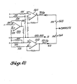
- FIGURE 4 is a detailed schematic diagram of the combiner circuits 92,94 shown in FIGURE 1.
- the design of the combiner circuit whether used in the localizer, as with combiner 92 or glideslope, combiner 94 of FIGURE 1, is the same. Thus, the design of a single combiner is shown.
- lines 500 and 502 receive the constant level 90 hertz and 150 hertz tones from the generator. The amplitudes of each of the tones is at the same fixed level. Also received from the generator is a 5.5 volt reference on line 504 and an 11 volt reference on line 506. The analog output signal from either the converter 340 on line 350 of the localizer circuit shown in FIGURE 2 or the converter 450 on the output line 452 of the circuit shown in FIGURE 3 is fed to the combiner via a line 508.
- the fixed level 90 hertz and 150 hertz tones are fed, respectively, to the V inputs, at pin 7 of a pair of divider modules 520, 522 respectively.
- the analog signal on line 508 is fed directly to the Vy input, pin 13, of divider module 520 whereas a differential amplifier stage indicated generally at reference 530 subtracts the analog signal appearing on line 508 from the 11 volt reference on 506, applying the resultant to the V input, at pin 13, of divider module 522.
- the 5.5 volt reference on line 504 is fed directly to the V x inputs, at pin 1, of each of the two divider modules 520,522. Also shown are offset circuits 536,537 which are fed to pin 5 of each of the modules 520, 522.
- the divider modules 520,522 in this, the preferred embodiment of the invention are Burr Brown type 4302 dividers, which are readily commercially available.
- the dividers 520, 522 produce an output signal, at pin 6, according to the following equation;
- the signal at pin 2 of divider module 420 is proportional to the analog signal on line 508 times the 90 hertz signal on line 500 whereas the output at pin 2 of divider module 522 is proportional to 11 volts minus the analog level on line 508 times the 150 hertz signal level.
- differential amplifiers 540 and 550 are summed with DC error correction signals produced by differential amplifiers 540 and 550 into summing amplifiers 560, 562.
- the function of the differential amplifiers 540, 550 is to restore the 5.5 volt DC reference level present in the NAV-401L receiver to the output of the combiner.circuit. It should be noted that each of the amplifiers utilized in the circuits of 530, 540, 550, 560 and 562 are commercially available LM 308 integrated circuits.
- the output from summing amplifier 560 is proportional to the 90 hertz reference level input times the control signal from the digital to analog converter whereas the output from amplifier 562 is proportional to the fixed 150 hertz reference times 11 volts minus the digital to analog converter output signal.
- These two signals are summed in summing resistors 563 and 564 producing an output composite signal which is of constant amplitude and has controlled proportions of the 90 hertz and 150 hertz signals in response to the output from the digital to analog converter.
- This composite signal is, thus, seen to be the information signal of either the localizer or glideslope which is ten routed to the NAV-401L generator where it modulates the appropriate carrier.
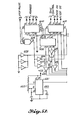
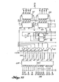
- FIGURE 5A and B are detailed schematic, diagrams of the VOR/marker tone circuit 24 shown in FIGURE 1.
- an address is received on lines 3-6 of the 40 line bus 16.
- the address is coupled into the inputs of a type 74L85 comparator 600.
- the comparator is wired such that when the signal at its input pins 10, 7, 2 and 15 is equal to the signal present at its input pins 11, 9, 1 and 14 equality is detected and pin 3 goes high.
- pins 11 and 14 connect to a high level as determined by the inverter bank 602. Pins 9 and 14, as shown, are grounded.Thus, the reference address is 1010. With a 1010 appearing at the address input, a quality is detected and pins 10 and 11 of NAND gate 604 go. high.
- pin 9 of NAND gate 604 goes high thus producing a low level pulse at pin 8.
- This low level pulse is inverted by parallel inverters 606 and 607, which are used to increase fanout, and are coupled to pin 8 of each of 7 type 74L95 registers 610-617.
- Pins 7 and 8 of the 40 line bus 16 determine which of four possible tones are generated, with pin 9 determining whether or not a marker beacon is on and pin 10 determining whether or not the VOR is on.
- the final condition is for high levels at both lines 7 and 8 of bus 16. Under this condition, pins 9 and 10 of register 610 go high resulting in pin 4 of decoder 630 being driven low. This is inverted by an inverter 639 and buffered by a buffer 640 thereby driving pin 12 of switching circuit 634.
- Line 9 of the bus 16 determines whether or not a marker tone should be turned on. With line 9 high, pin 12 of register 610 is high which, due to the buffers 641-643, drives pins 13, 5 and 6 of switching circuit 650. As described more fully herein below, switching circuit 640 is wired to the generator such that upon pins 13, 5 and 6 being driven the marker tone is turned on.
- Line 10 of the bus 16 determines whether or not the VOR circuitry within the generator is to be activated. When line 10 goes high, pin 13 of register 610 is driven high which, via buffers 651-653, drives pin 12 of switching circuit 650 and pins 13 and 5 of switching circuit 655.
- a 500 hertz generator indicated generally at 660 is comprised of a type 555 integrated circuit 661 and associated timing circuitry, indicated generally at 662 which determine the frequency of oscillation.
- Produced at pin 3 of 555 integrated circuit 661 is the 500 hertz signal. This signal is passed to the input, at pin 9, of the divider 618. Loaded into the divider 618 is a first divisor N 1 from register 611.
- the 500 hertz signal is divided in frequency by a factor N and passed, via output pin 5 to the input, at pin 9, of the second divider 619. Contained within the second divider 619 is a second divisor N 2 which has been loaded via register 612. The divisors in the registers 611, 612 are sourced via lines 11-18 of the 40 line bus 16.
- Lines 19 through 32 of the 40 line bus 16 determine the final VOR bearing. These are loaded into registers 613-617 and, upon the addressing circuitry determining that the VOR is being addressed, are compared via a sequence of comparators 620-623 to the present VOR bearing value as stored in a sequence of BCD counters 680-683.
- the BCD counters in this, the preferred embodiment of the invention, are comprised of type 74LS192, commercially available integrated circuits.
- Line 37 of the 40 line bus 16 is a computer input indicating whether the final VOR bearing value should be approached from the clockwise or counter clockwise direction. Thus, if line 37 is low, pine 12 of register 617 goes low causing a low to appear at pin 3 of NAND gate 671 and a high, through inverter 690, to appear at pin 1 of NAND gate 670.
- the comparator chain 620-623 is wired to produce a high at pin 3 of final comparator 623 only for the condition wherein the desired final values, as stored in registers '613-617, exactly equals the present value in counters 680-683.
- the status at pin 3 of comparator 623 is monitored at pin 13 of NAND gate 670 and at pin 5 of NAND gate 671.
- VOR bearing circuitry Operation of the VOR bearing circuitry may be understood as follows.
- a desired new bearing setting as determined by the computer, is loaded into the register 613-617.
- the computer also drives line 17 of bus 16 either high or low to determine whether or not the new bearing value should be approached from the clockwise or counter clockwise rotation. If the desired final value differs from the present VOR value, pin 3 of comparator 623 is low and, if the clockwise direction of approaching the final value bearing is desired, then pin 2 of NAND gate 670 is low resulting in a high at its pin 12 which causes the counter 680-683 to begin counting up at the rate 500 hertz/N.
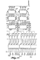
- FIGURE 9 shows modifications added to FIGURES 5A, B to confine the counting range to 0°-360°.
- configuring as per FIGURES 5A, B allows a count up/count down range of 0°-400°.
- .U34 and U35 are 7485 comparators added across the output of U18 and U19.
- the 'B' side of the comparator is hardwired for an input of 360°.
- a count of 360.0 causes a high to be output on pin 6 of U35 which forces all counters to be 0 0 (zero) .
- This event (clearing) is configured to occur on count-up or clockwise (cw) direction.
- the instantaneous VOR bearing value, as determined in counters 680-683, is constantly sensed and used to drive corresponding circuitry in the NAV-401L generator.
- the present status of the counter 680 is buffered via buffers 700-703 and drives inputs 6 and 12 of switching circuit 655 and 13 and 5 of switching circuit 710.
- the present status of counter 681 is buffered through buffers 711-714 and applied to pin 6 and 12 of switching circuit 712 and 13 and 5 of switching circuit 715.
- the present value in counter 682 is buffered through buffers 716-719 and used to drive pins 6 and 12 of switching circuit 715 and pins 13 and 5 of switching circuit 720.
- the instantaneous values in counter 683 are buffered via buffers 721 and 722 and are used to drive pins 6 and 12 of switching circuit 720.
- the switching circuits 634, 650, 655, 710, 715 and 720 are comprised of commercially available type CD 4016AE devices. These devices require a bank of pullup resistors, one of which is indicated by reference 730, each of which couples an input pin to the 15 volt supply.
- switch outputs couple through output pins, as shown, and connect through terminals, numbered 43-74 of an output plug, indicated generally at 740.
- This plug in turn couples to a connector, described more fully with respect to FIGURES 6, 7 and 8, on a modified NAV-401L generator.
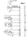
- FIGURES 6, 7 and 8 detail modifications to a standard NAV-401L generator.
- modifications are shown to a NAV-401L to automate VOR and marker beacon generation.
- Switch S7 which controls the audio tones for VOR and marker beacon, is left in the off position for automatic operation.
- Switch S701 is a three segment switch which routes signals, internal to the generator, to the proper NAV-401L circuits to place the generator in the marker beacon, VOR, localizer, glideslope or VHF communication generation mode.
- the input to the rotary portion of the switch segments has been cut and brought to the interface connector.
- only the portions of the switch segments controlling marker beacon crystal and VOR crystal modes of operation have been brought to the interface bus connector. This creates a generator which can be controlled automatically to output all VOR and marker beacon signals, but not any other modes.
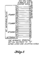
- FIGURE 8 shows the thumbwheel switches on the NAV-401L which are normally used in manual operation to select the desired bearing output using a BCD format. Duplicate wires are brought out to the automatic interface. In the automatic mode of operation, the switches are all set to 0 (zero) or "open" position and closure is then performed via the CMOS switches 655, 710, 715, 720 shown in FIGURES 5A, B.
- FIGURE 7 shows modifications to a NAV-401L to allow automatic control of localizer and glideslope.
- the 90 Hz and 150 Hz tones are removed from the manual control potention- meters R5 (localizer) and R7 (glideslo p e) and routed to the interface connector. From there, they are input via lines 123 and 125 on FIGURE 1 to the combiner printed circuit board. After being processes as previously described, they are routed back to the potentiometers-in the NAV-401L. This allows the potentiometers to be used to null out tolerance errors in the aircraft receivers.
- Switch S701 is modified as described in the VOR/ marker beacon explanation, except that the control is now of the localizer crystal mode and glideslope crystal mode.
- Both the VOR/MKR and LOC/GS configured NAV-401L generators are supplies with a jumper plug, shown in FIGURES 6 and 7, which when plugged into the interface connectors, serve to defeat the internal modification. This allows removal of a generator from the automatic test equipment bay for normal use in the manual mode for all functions of the generator.
Landscapes
- Engineering & Computer Science (AREA)
- Computer Networks & Wireless Communication (AREA)
- Physics & Mathematics (AREA)
- General Physics & Mathematics (AREA)
- Radar, Positioning & Navigation (AREA)
- Remote Sensing (AREA)
- Feedback Control In General (AREA)
- Control Of Position, Course, Altitude, Or Attitude Of Moving Bodies (AREA)
Priority Applications (2)
| Application Number | Priority Date | Filing Date | Title |
|---|---|---|---|
| EP19800201100 EP0052671B1 (de) | 1980-11-20 | 1980-11-20 | Automatischer Simulator für Flugzeugfunknavigationssignale |
| DE8080201100T DE3071558D1 (en) | 1980-11-20 | 1980-11-20 | Automated aircraft radio navigation simulator |
Applications Claiming Priority (1)
| Application Number | Priority Date | Filing Date | Title |
|---|---|---|---|
| EP19800201100 EP0052671B1 (de) | 1980-11-20 | 1980-11-20 | Automatischer Simulator für Flugzeugfunknavigationssignale |
Publications (2)
| Publication Number | Publication Date |
|---|---|
| EP0052671A1 true EP0052671A1 (de) | 1982-06-02 |
| EP0052671B1 EP0052671B1 (de) | 1986-04-16 |
Family
ID=8187052
Family Applications (1)
| Application Number | Title | Priority Date | Filing Date |
|---|---|---|---|
| EP19800201100 Expired EP0052671B1 (de) | 1980-11-20 | 1980-11-20 | Automatischer Simulator für Flugzeugfunknavigationssignale |
Country Status (2)
| Country | Link |
|---|---|
| EP (1) | EP0052671B1 (de) |
| DE (1) | DE3071558D1 (de) |
Cited By (1)
| Publication number | Priority date | Publication date | Assignee | Title |
|---|---|---|---|---|
| EP0778469A1 (de) * | 1995-12-08 | 1997-06-11 | AEROSPATIALE Société Nationale Industrielle | Verfahren und Vorrichtung zum Prüfen von Funknavigationsgeräten mit Messgeräten und Generatoren für Normsignale |
Families Citing this family (2)
| Publication number | Priority date | Publication date | Assignee | Title |
|---|---|---|---|---|
| DE19722913A1 (de) * | 1997-05-31 | 1998-12-03 | Alsthom Cge Alcatel | Gleitweg-Sendeeinrichtung für das Instrumentenlandesystem ILS |
| US10318677B2 (en) | 2014-03-17 | 2019-06-11 | Textron Innovations, Inc. | Synthesis of radio frequency environment |
Citations (5)
| Publication number | Priority date | Publication date | Assignee | Title |
|---|---|---|---|---|
| US3358284A (en) * | 1964-12-28 | 1967-12-12 | Cossor Ltd A C | Radio-frequency source for simulating vor signals |
| US3413638A (en) * | 1964-12-24 | 1968-11-26 | Cossor Ltd A C | Electrical phase-locking circuits |
| US3805588A (en) * | 1970-07-17 | 1974-04-23 | N Stone | Apparatus for producing output test signals for testing aircraft instrument landing system and navigation equipment |
| US3845484A (en) * | 1973-06-12 | 1974-10-29 | Bendix Corp | Signal generator for testing vor navigation receivers |
| FR2398350A1 (fr) * | 1977-07-20 | 1979-02-16 | Aerospatiale | Dispositif pour la simulation de signaux de reperage emis par une balise |
-
1980
- 1980-11-20 EP EP19800201100 patent/EP0052671B1/de not_active Expired
- 1980-11-20 DE DE8080201100T patent/DE3071558D1/de not_active Expired
Patent Citations (5)
| Publication number | Priority date | Publication date | Assignee | Title |
|---|---|---|---|---|
| US3413638A (en) * | 1964-12-24 | 1968-11-26 | Cossor Ltd A C | Electrical phase-locking circuits |
| US3358284A (en) * | 1964-12-28 | 1967-12-12 | Cossor Ltd A C | Radio-frequency source for simulating vor signals |
| US3805588A (en) * | 1970-07-17 | 1974-04-23 | N Stone | Apparatus for producing output test signals for testing aircraft instrument landing system and navigation equipment |
| US3845484A (en) * | 1973-06-12 | 1974-10-29 | Bendix Corp | Signal generator for testing vor navigation receivers |
| FR2398350A1 (fr) * | 1977-07-20 | 1979-02-16 | Aerospatiale | Dispositif pour la simulation de signaux de reperage emis par une balise |
Non-Patent Citations (3)
| Title |
|---|
| IEEE Transactions on Aerospace and Electronic Systems, Vol. AES-9, No. 1, January 1973 New York, US Y. NEUVO: "The Application of Digital Techniques to a VOR Signal Generator", pages 38-42 * thw whole document * * |
| Marconi Instrumentation, Vol. 14, No. 5, October 1974 Longacres, St. Albans, Herts, GB G.M. COLEBOURN: "Precision Amplitude Modulators for VOR-ILS Receiver", pages 98-102 * page 100, right-hand column the paragraph: "Receiver Testing - page 102, right-hand column last line; figures 4-7 * * |
| Navy Technical Disclosure Bulletin, Vol. 3, No. 3, March 1978 Arlington, GB T.C. PENDERGRAFT: "Radar Signature Generator", pages 1-5 *the whole document * * |
Cited By (3)
| Publication number | Priority date | Publication date | Assignee | Title |
|---|---|---|---|---|
| EP0778469A1 (de) * | 1995-12-08 | 1997-06-11 | AEROSPATIALE Société Nationale Industrielle | Verfahren und Vorrichtung zum Prüfen von Funknavigationsgeräten mit Messgeräten und Generatoren für Normsignale |
| FR2742232A1 (fr) * | 1995-12-08 | 1997-06-13 | Sextant Avionique | Procede et dispositif pour le test d'instruments de radio-navigation utilisant des appareils de mesure et de generation de signaux standards |
| US5790438A (en) * | 1995-12-08 | 1998-08-04 | Aerospatiale Societe Nationale Industrielle | Radio navigation testing method and device using standard signal measuring and generating equipment |
Also Published As
| Publication number | Publication date |
|---|---|
| EP0052671B1 (de) | 1986-04-16 |
| DE3071558D1 (en) | 1986-05-22 |
Similar Documents
| Publication | Publication Date | Title |
|---|---|---|
| US2560527A (en) | Apparatus for simulating radio navigation aids | |
| US2471315A (en) | Aircraft trainer for aerial gunners | |
| US4311466A (en) | Automated aircraft radio navigation simulator | |
| US2560528A (en) | Training means for blind navigating systems | |
| US3832712A (en) | Doppler signal simulator | |
| EP0052671B1 (de) | Automatischer Simulator für Flugzeugfunknavigationssignale | |
| US2559039A (en) | Simulated radio direction finding means for aviation trainers | |
| US3665086A (en) | Loran trainer | |
| US2811788A (en) | Simulated radio navigation apparatus | |
| US3020651A (en) | Automatic magnetic deviation effects in flight simulators | |
| US4400789A (en) | Magnetic heading simulator | |
| US3500439A (en) | Simulation of radio navigation equipment | |
| US3663734A (en) | Simulated aircraft radio aids | |
| GB1291211A (en) | Simulation of instruments in a fixed-base aircraft trainer | |
| US2889635A (en) | Artificial aircraft simulator for radar systems | |
| JPH0231352B2 (de) | ||
| US2774149A (en) | Radar trainer | |
| USRE23627E (en) | Apparatus fob simulating radio | |
| US2890442A (en) | Failure warning systems for navigational apparatus | |
| JPH033191B2 (de) | ||
| US2721397A (en) | Simulated high frequency radio receiving apparatus for aircraft trainers | |
| US3026038A (en) | Chart recording system | |
| US2457130A (en) | Blind flying and blind landing system for aviation flight trainers | |
| US3862717A (en) | Method and apparatus for automatically computing vertical track angle | |
| US3034228A (en) | Vectoring phase simulator |
Legal Events
| Date | Code | Title | Description |
|---|---|---|---|
| PUAI | Public reference made under article 153(3) epc to a published international application that has entered the european phase |
Free format text: ORIGINAL CODE: 0009012 |
|
| AK | Designated contracting states |
Designated state(s): DE FR GB IT NL SE |
|
| 17P | Request for examination filed |
Effective date: 19821130 |
|
| ITF | It: translation for a ep patent filed | ||
| GRAA | (expected) grant |
Free format text: ORIGINAL CODE: 0009210 |
|
| AK | Designated contracting states |
Kind code of ref document: B1 Designated state(s): DE FR GB IT NL SE |
|
| PG25 | Lapsed in a contracting state [announced via postgrant information from national office to epo] |
Ref country code: SE Effective date: 19860430 |
|
| REF | Corresponds to: |
Ref document number: 3071558 Country of ref document: DE Date of ref document: 19860522 |
|
| ET | Fr: translation filed | ||
| PLBE | No opposition filed within time limit |
Free format text: ORIGINAL CODE: 0009261 |
|
| STAA | Information on the status of an ep patent application or granted ep patent |
Free format text: STATUS: NO OPPOSITION FILED WITHIN TIME LIMIT |
|
| 26N | No opposition filed | ||
| PGFP | Annual fee paid to national office [announced via postgrant information from national office to epo] |
Ref country code: GB Payment date: 19901030 Year of fee payment: 11 |
|
| PGFP | Annual fee paid to national office [announced via postgrant information from national office to epo] |
Ref country code: FR Payment date: 19901129 Year of fee payment: 11 |
|
| ITTA | It: last paid annual fee | ||
| PGFP | Annual fee paid to national office [announced via postgrant information from national office to epo] |
Ref country code: NL Payment date: 19901130 Year of fee payment: 11 |
|
| PGFP | Annual fee paid to national office [announced via postgrant information from national office to epo] |
Ref country code: DE Payment date: 19901221 Year of fee payment: 11 |
|
| PG25 | Lapsed in a contracting state [announced via postgrant information from national office to epo] |
Ref country code: GB Effective date: 19911120 |
|
| PG25 | Lapsed in a contracting state [announced via postgrant information from national office to epo] |
Ref country code: NL Effective date: 19920601 |
|
| GBPC | Gb: european patent ceased through non-payment of renewal fee | ||
| NLV4 | Nl: lapsed or anulled due to non-payment of the annual fee | ||
| PG25 | Lapsed in a contracting state [announced via postgrant information from national office to epo] |
Ref country code: FR Effective date: 19920731 |
|
| PG25 | Lapsed in a contracting state [announced via postgrant information from national office to epo] |
Ref country code: DE Effective date: 19920801 |
|
| REG | Reference to a national code |
Ref country code: FR Ref legal event code: ST |