EP0053654A2 - Cellule de mémoire à un transistor de grande capacité utilisable comme mémoire à accès aléatoire - Google Patents
Cellule de mémoire à un transistor de grande capacité utilisable comme mémoire à accès aléatoire Download PDFInfo
- Publication number
- EP0053654A2 EP0053654A2 EP81106695A EP81106695A EP0053654A2 EP 0053654 A2 EP0053654 A2 EP 0053654A2 EP 81106695 A EP81106695 A EP 81106695A EP 81106695 A EP81106695 A EP 81106695A EP 0053654 A2 EP0053654 A2 EP 0053654A2
- Authority
- EP
- European Patent Office
- Prior art keywords
- layer
- doped
- gate
- capacitor
- nitride
- Prior art date
- Legal status (The legal status is an assumption and is not a legal conclusion. Google has not performed a legal analysis and makes no representation as to the accuracy of the status listed.)
- Withdrawn
Links
- 230000015654 memory Effects 0.000 title claims abstract description 27
- 239000003990 capacitor Substances 0.000 claims abstract description 102
- 229910021420 polycrystalline silicon Inorganic materials 0.000 claims abstract description 97
- 229920005591 polysilicon Polymers 0.000 claims abstract description 97
- 150000004767 nitrides Chemical class 0.000 claims abstract description 76
- 239000000758 substrate Substances 0.000 claims abstract description 68
- XUIMIQQOPSSXEZ-UHFFFAOYSA-N Silicon Chemical compound [Si] XUIMIQQOPSSXEZ-UHFFFAOYSA-N 0.000 claims abstract description 50
- 229910052710 silicon Inorganic materials 0.000 claims abstract description 50
- 239000010703 silicon Substances 0.000 claims abstract description 50
- VYPSYNLAJGMNEJ-UHFFFAOYSA-N Silicium dioxide Chemical compound O=[Si]=O VYPSYNLAJGMNEJ-UHFFFAOYSA-N 0.000 claims abstract description 36
- 229910052814 silicon oxide Inorganic materials 0.000 claims abstract description 34
- 238000000034 method Methods 0.000 claims abstract description 20
- 230000005669 field effect Effects 0.000 claims abstract description 8
- 229910052594 sapphire Inorganic materials 0.000 claims abstract description 7
- 239000010980 sapphire Substances 0.000 claims abstract description 7
- 239000002019 doping agent Substances 0.000 claims description 10
- 238000004519 manufacturing process Methods 0.000 claims description 9
- 239000011521 glass Substances 0.000 claims description 8
- OAICVXFJPJFONN-UHFFFAOYSA-N Phosphorus Chemical compound [P] OAICVXFJPJFONN-UHFFFAOYSA-N 0.000 claims description 7
- 239000011248 coating agent Substances 0.000 claims description 7
- 238000000576 coating method Methods 0.000 claims description 7
- 230000000873 masking effect Effects 0.000 claims description 7
- 229910052698 phosphorus Inorganic materials 0.000 claims description 7
- 239000011574 phosphorus Substances 0.000 claims description 7
- 239000004020 conductor Substances 0.000 claims description 6
- 239000004065 semiconductor Substances 0.000 claims description 4
- 238000000151 deposition Methods 0.000 claims description 3
- 230000005855 radiation Effects 0.000 claims description 2
- 230000001965 increasing effect Effects 0.000 abstract description 5
- 210000004027 cell Anatomy 0.000 description 27
- 238000003860 storage Methods 0.000 description 6
- 239000000463 material Substances 0.000 description 4
- 229920002120 photoresistant polymer Polymers 0.000 description 4
- 239000007943 implant Substances 0.000 description 3
- 238000010276 construction Methods 0.000 description 2
- 230000002708 enhancing effect Effects 0.000 description 2
- 238000005530 etching Methods 0.000 description 2
- 150000002500 ions Chemical class 0.000 description 2
- ZOXJGFHDIHLPTG-UHFFFAOYSA-N Boron Chemical compound [B] ZOXJGFHDIHLPTG-UHFFFAOYSA-N 0.000 description 1
- OWNRRUFOJXFKCU-UHFFFAOYSA-N Bromadiolone Chemical compound C=1C=C(C=2C=CC(Br)=CC=2)C=CC=1C(O)CC(C=1C(OC2=CC=CC=C2C=1O)=O)C1=CC=CC=C1 OWNRRUFOJXFKCU-UHFFFAOYSA-N 0.000 description 1
- 101100269850 Caenorhabditis elegans mask-1 gene Proteins 0.000 description 1
- 230000015572 biosynthetic process Effects 0.000 description 1
- 229910052796 boron Inorganic materials 0.000 description 1
- 239000003989 dielectric material Substances 0.000 description 1
- 238000009792 diffusion process Methods 0.000 description 1
- 238000005516 engineering process Methods 0.000 description 1
- 238000002513 implantation Methods 0.000 description 1
- 239000012212 insulator Substances 0.000 description 1
- 230000014759 maintenance of location Effects 0.000 description 1
- 239000002184 metal Substances 0.000 description 1
- 229910021421 monocrystalline silicon Inorganic materials 0.000 description 1
- 230000001590 oxidative effect Effects 0.000 description 1
- 230000003071 parasitic effect Effects 0.000 description 1
- 235000012239 silicon dioxide Nutrition 0.000 description 1
- 239000000377 silicon dioxide Substances 0.000 description 1
- 239000007787 solid Substances 0.000 description 1
- 238000010025 steaming Methods 0.000 description 1
- 210000000352 storage cell Anatomy 0.000 description 1
Images


Classifications
-
- H—ELECTRICITY
- H10—SEMICONDUCTOR DEVICES; ELECTRIC SOLID-STATE DEVICES NOT OTHERWISE PROVIDED FOR
- H10D—INORGANIC ELECTRIC SEMICONDUCTOR DEVICES
- H10D1/00—Resistors, capacitors or inductors
- H10D1/60—Capacitors
- H10D1/68—Capacitors having no potential barriers
-
- H—ELECTRICITY
- H10—SEMICONDUCTOR DEVICES; ELECTRIC SOLID-STATE DEVICES NOT OTHERWISE PROVIDED FOR
- H10B—ELECTRONIC MEMORY DEVICES
- H10B12/00—Dynamic random access memory [DRAM] devices
- H10B12/30—DRAM devices comprising one-transistor - one-capacitor [1T-1C] memory cells
Definitions
- the invention relates to a novel structure and method for forming a high capacitance and a single transistor capable of use as a memory cell for high density RAM applications.
- the invention comprises a high capacity memory cell including a gating transistor.
- the silicon substrata may be used or a sapphire substrate with a silicon layer thereon.
- a doped polysilicon layer is disposed adjacent the silicon for forming a junction therein with a patterned nitride layer adjacent the doped polysilicon layer and a further polysilicon layer adjacent the nitride layer such that the capacitor so formed has a capacity four times as great as a conventional silicon oxide and poly capacitor and is increased to six times as great when the junction capacity and nitride capacity are added, thus providing a very substantial savings in real estate on the chip.
- a field effect transistor is added to the capacitor by silicon oxide covered by polysilicon with doping extending between the capacitor and the gate region to connect electrically with the junction while providing the drain, the source being a doped region on the other side of the gate.
- the method of forming capacitance memory cells is unique in that each gate is formed as a layer of gate oxide with a layer of doped polysilicon thereover, doped substrate regions are formed on opposite sides of the gate to comprise a transistor with the doped substrate region on one side of the gate being in electrical connection with the junction doped region on said one side of the gate, which junction lies under a layer of doped polysilicon covered by a layer of nitride, in turn covered by a second layer of doped polysilicon to comprise the capacitor.
- the present invention provides a new technique which enables the reduction in area for a memory cell without any penalties in storage capacitance. Additionally, this invention is fully compatible with the existing processing practices and provides a novel capacitor structure.
- doped polysilicon makes contact with single crystal silicon to make a "buried" structure which enables the diffusion of dopant from the polysilicon source into the bulk silicon to form a junction.
- this first layer of polysilicon forms the transfer gate of the memory cell.
- Nitride is left on top of the polysilicon once it has been patterned.
- This thin layer of nitride represents the dielectric material that will comprise the capacitor insulator between the first polysilicon layer and the second polysilicon layer.
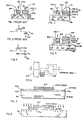
- FIG. 1 wherein the prior art conventional memory cell structure is shown as comprising the transfer gate 101 and a memory capacitor 103.
- a silicon substrate 105 is provided which is oxidized to form the silicon oxide 107 underneath the gate polysilicon 109 for the gate transistor 101 and the silicon dioxide 109 underneath the polysilicon 111 forming the capacitor 103.
- the source region 113 and drain region 115 are doped and the capacitor structure is capable of forming the temporary junction 119 beneath the silicon oxide layer 109 in the silicon substrate 105,which junction is in electrical connection with the drain doped region 115.
- the equivalent circuit for the structure shown in FIG. 1 is shown in FIG. 3 as comprising the transfer or gating transistor 101 and the capacitor 103.
- the junction or inversion layer 119 beneath capacitor 103 in the structure of FIG. 1 is only there when the positive voltage is applied to the capacitor lead 121.
- the structure of FIG. 2 provides a permanent junction 151 because the doped polysilicon I layer 153 is in direct contact with the surface of the silicon substrate 155 and the dopant is diffused into the bulk silicon to form a junction.
- This same layer of poly I, shown at 153 forms the transfer gate polysilicon layer 159 over a thin layer of silicon oxide 161.
- the doped n+ region 163 is the source and the doped n+ region 165 is the drain which region is in electrical contact with the junction region 151.
- the thin layer of nitride 169 forms the dielectric for the capacitance which structure is completed by the poly II layer 171.
- the ground lead 173 for poly II layer 171 enables the junction capacitor and the nitride capacitor to be connected in parallel, thereby considerably enhancing the capacitance obtained from the structure of FIG. 2.
- the electrical circuit is shown in FIG. 4 where C2 is the combined capacitance of the junction and the nitride layer, but otherwise the circuit is the same as the memory cell circuit of FIG. 3 using transfer gate 201 for determining access to capacitor 203.
- the total capacitance per unit area is given by C j + C where C j is the junction capacitance and C n is the nitride capacitance.
- C n ⁇ n /t n for the nitride capacitor wherein En is about two times higher than ⁇ ox and t n can usually be a thinner layer than that used for an oxide capacitor, therefore enhancing the value of C n .
- C j is given by .
- C 2 is therefore equal to (Cj + C n ) x A where A is the capacitor.
- C is much greater than C ox since ⁇ n is greater than ⁇ ox and t n is less than t ox ⁇ 0
- the t equalling approximately 400 A and t ox approximately 4 C ox .
- the junction capacitance increases C 2 to a value equivalent to 6 C 1 .
- the area of a memory cell capacitor can be reduced by a factor of 6 times without any decrease in storage capacitance.
- reduction in the cell area usually results in shorter column bit lines so that the ratio of the storage cell capacitance to bit line parasitic capacitance is increased, thereby providing a larger sense signal to the sense amplifier inputs.
- the decay rate of the storage charge in the cell is proportional to the area of the capacitor.
- the top electrode, the second poly layer 171 of the storage capacitor is connected to the ground potential, as shown by lead 173. This arrangement provides better reliability than the conventional configuration where the top electrode 121 is connected to the most positive supply, usually Y dd , because of less severe DC supply and no field inversion problems.
- FIG. 5 which merely shows a silicon on sapphire structure patterned after the structure on silicon of FIG. 2, thus the prime of the numbers applied to the structure of FIG. 2 will be used in FIG. 5.
- the sapphire substrate is shown at 211 and the silicon layer at 155'.
- the capacitor comprises the poly I layer 153', the thin nitride layer 169', the poly II layer 171' and the grounding lead 173'.
- the transfer transistor gate comprises a silicon oxide layer 161', the source 163' and the drain 165' with the capacitor junction 151' being located beneath the poly I layer 153'. Otherwise, the principles of operation heretofore explained obtain in the structure of FIG. 5.
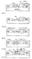
- FIGs. 7 through 23 One method is illustrated in FIGs. 7 through 23 wherein a substrate 501 of for example P(100) type silicon single or monocrystalline structure has grown thereon a thin silicon oxide layer 503, in turn covered by a nitride layer 505 and, as shown in FIG. 7.photoresist 507 defined by the active mask 509 shown in the solid outline in FIG. 6.
- the silicon oxide coating 503 is quite thin of the order of 100 A with the silicon 0 nitride coating 505 being of the order of 1000 A.
- the resist used in layer 507 may be AZ 1350J or HPR204 or equivalent.
- the field implant is shown by the xs identified at 511, the unprotected nitride 505 and silicon oxide 503 having been removed by appropriate etching techniques, boron or the like is used here to provide a heavily doped P region surrounding the active area of a device with n+ source and drains.
- the resist 507 has been removed and the field oxide grown at 513 which encircles the active region.
- the field oxide 513 may have a thickness of the order of 18.6 K angstroms.
- FIGURE 10 shows the outline of the capacitor region utilizing the capacitor mask -1 shown dotted at 521 in FIG. 6. First, the entire region is covered by the photoresist 523 and thereafter the mask 521 is utilized to open the region 525 to the bare silicon substrate using conventional processing techniques.
- FIG. 11 the n+ implanting of the region within substrate 501 below bare silicon surface 525 is accomplished by ion implant or the like. Note that in FIGs. 9 and 10, the nitride layer 505 has been etched away and the photoresist 523 applied directly to the silicon oxide layer.
- the implanting is preferably carried out by a high energy ion implant.
- the n+ region is indicated at 529.
- a layer of n+ doped polysilicon 531 is applied over the entire active area and is covered with a thin layer of nitride 533.
- the device is subjected to high temperature to drive the dopant in to increase the depth of the region 529.
- the gate capacitor mask consisting of dotted parts 535a and 535b in FIG. 13 is utilized to provide a resist pattern in accordance with FIG. 14 wherein the resist 537 defines the capacitive region and the resist 539, the gate region.
- the nitride and doped polysilicon layers 533 and 531 have been etched away where unprotected by the resist 537 and 539. Also, the region to the left of the gate region covered by resist 539 is implanted (or diffused) by n+ material in the area illustrated at 541 for the source region of the transistor being formed.
- the resist has been removed at 537 and 539 (FIG. 15) and a thin layer of oxide 540 grown over n+ region 529.
- FIG. 17 a layer of doped poly II silicon 551 is applied over the entire active area.
- FIGURE 18 shows the capacitor mask -2, shown dotted at 553 which is used to lay down a resist pattern shown in FIG. 19 wherein the poly II 551 which is preserved will comprise the outer plate of the capacitor structure being formed.
- the nitride has been removed from the gate polysilicon layer 532 and in FIG. 21 the entire structure has been covered by a layer of phosphorus doped glass 561.
- the purpose of the glass is to form a high resistivity layer over the components to isolate them when terminal connections are provided.
- FIG. 22 it may be seen that an opening has been made to the n+ source region 541 as represented at 572. Also, an opening 573 has been made to the top of the polysilicon 532 comprising a gate. Finally, an opening has been made to the polysilicon 551 comprising the capacitor and is shown at 574.
- These openings are filled by a metal to provide the source conductor shown at 591 in FIG. 23, the gate conductor 592, and the capacitance conductor 593.
- the latter may simply be grounded to provide the capacitive addition.
- a standard opening technique is applied where masking is used to protect the remaining surface while allowing etching to take place in the areas to be opened.
- the invention may be summarized as follows:
Landscapes
- Semiconductor Memories (AREA)
- Semiconductor Integrated Circuits (AREA)
Applications Claiming Priority (2)
| Application Number | Priority Date | Filing Date | Title |
|---|---|---|---|
| US21278480A | 1980-12-04 | 1980-12-04 | |
| US212784 | 1988-06-29 |
Publications (2)
| Publication Number | Publication Date |
|---|---|
| EP0053654A2 true EP0053654A2 (fr) | 1982-06-16 |
| EP0053654A3 EP0053654A3 (en) | 1983-03-30 |
Family
ID=22792412
Family Applications (1)
| Application Number | Title | Priority Date | Filing Date |
|---|---|---|---|
| EP81106695A Withdrawn EP0053654A3 (en) | 1980-12-04 | 1981-08-28 | High capacitance single transistor memory cell suitable for high density ram applications |
Country Status (2)
| Country | Link |
|---|---|
| EP (1) | EP0053654A3 (fr) |
| JP (1) | JPS57106162A (fr) |
Cited By (2)
| Publication number | Priority date | Publication date | Assignee | Title |
|---|---|---|---|---|
| US6194274B1 (en) * | 1999-08-10 | 2001-02-27 | Winbond Electronics Corp. | Method of fabricating a mask ROM |
| US6432791B1 (en) * | 1999-04-14 | 2002-08-13 | Texas Instruments Incorporated | Integrated circuit capacitor and method |
-
1981
- 1981-08-28 EP EP81106695A patent/EP0053654A3/en not_active Withdrawn
- 1981-10-29 JP JP56175570A patent/JPS57106162A/ja active Pending
Non-Patent Citations (3)
| Title |
|---|
| IBM TECHNICAL DISCLOSURE BULLETIN, Vol. 23, No. 12, May 1981, New York. P. DUN et al: "High capacitance RAM cell using two layers of polysilicon", pages 5290 to 5291 * |
| IEEE TRANSACTIONS ON ELECTRON DEVICES, Vol. ED-23, No. 10, October 1976, New York. C.G. SODINI et al: "Ehanced capacitor for one-transistor memory cell", pages 1187 to 1189 * |
| IEEE TRANSACTIONS ON ELECTRON DEVICES, Vol. ED-27, No. 8, August 1980, New York. M. KOYANAGI et al: "A 5-V only 16-kbit stacked-capacitor MOS RAM", pages 1596 to 1601 * |
Cited By (2)
| Publication number | Priority date | Publication date | Assignee | Title |
|---|---|---|---|---|
| US6432791B1 (en) * | 1999-04-14 | 2002-08-13 | Texas Instruments Incorporated | Integrated circuit capacitor and method |
| US6194274B1 (en) * | 1999-08-10 | 2001-02-27 | Winbond Electronics Corp. | Method of fabricating a mask ROM |
Also Published As
| Publication number | Publication date |
|---|---|
| EP0053654A3 (en) | 1983-03-30 |
| JPS57106162A (en) | 1982-07-01 |
Similar Documents
| Publication | Publication Date | Title |
|---|---|---|
| US4314857A (en) | Method of making integrated CMOS and CTD by selective implantation | |
| CA1079866A (fr) | Cellules de memoire a un fet et a deux couches de silicium polycristallin | |
| US5807778A (en) | Method of manufacturing shallow trench source EPROM cell | |
| US4252579A (en) | Method for making single electrode U-MOSFET random access memory utilizing reactive ion etching and polycrystalline deposition | |
| US4931847A (en) | Floating gate memory with sidewall tunnelling area | |
| US4178674A (en) | Process for forming a contact region between layers of polysilicon with an integral polysilicon resistor | |
| US4566175A (en) | Method of making insulated gate field effect transistor with a lightly doped drain using oxide sidewall spacer and double implantations | |
| US4804637A (en) | EEPROM memory cell and driving circuitry | |
| US4364074A (en) | V-MOS Device with self-aligned multiple electrodes | |
| US5162890A (en) | Stacked capacitor with sidewall insulation | |
| US4717942A (en) | Dynamic ram with capacitor groove surrounding switching transistor | |
| US5668391A (en) | Vertical thin film transistor | |
| US5492851A (en) | Method for fabricating attached capacitor cells in a semiconductor device having a thin film transistor | |
| US5017515A (en) | Process for minimizing lateral distance between elements in an integrated circuit by using sidewall spacers | |
| WO1992010002A1 (fr) | Memoire eeprom de faible largeur avec formation des electrodes par diffusion en une seule etape | |
| US4975383A (en) | Method for making an electrically erasable programmable read only memory cell having a three dimensional floating gate | |
| DE68922424T2 (de) | Ladungsverstärkende Grabenspeicherzelle. | |
| JPH03129769A (ja) | ダイナミックram記憶素子及び製造方法 | |
| EP0028654B1 (fr) | Dispositif de memoire a semi-conducteur et son procede de fabrication | |
| US6040209A (en) | Semiconductor memory device and method of forming transistors in a peripheral circuit of the semiconductor memory device | |
| US5245212A (en) | Self-aligned field-plate isolation between active elements | |
| EP0034508A1 (fr) | Contact auto-alignant profond et procédé pour sa fabrication | |
| US4357747A (en) | Method for producing a semiconductor device having an insulated gate type field effect transistor | |
| EP0053654A2 (fr) | Cellule de mémoire à un transistor de grande capacité utilisable comme mémoire à accès aléatoire | |
| KR100261210B1 (ko) | 디커플링 커패시터의 형성방법 |
Legal Events
| Date | Code | Title | Description |
|---|---|---|---|
| PUAI | Public reference made under article 153(3) epc to a published international application that has entered the european phase |
Free format text: ORIGINAL CODE: 0009012 |
|
| 17P | Request for examination filed |
Effective date: 19811023 |
|
| AK | Designated contracting states |
Designated state(s): DE FR GB IT |
|
| PUAL | Search report despatched |
Free format text: ORIGINAL CODE: 0009013 |
|
| AK | Designated contracting states |
Designated state(s): DE FR GB IT |
|
| STAA | Information on the status of an ep patent application or granted ep patent |
Free format text: STATUS: THE APPLICATION IS DEEMED TO BE WITHDRAWN |
|
| 18D | Application deemed to be withdrawn |
Effective date: 19850302 |
|
| RIN1 | Information on inventor provided before grant (corrected) |
Inventor name: TAM, MATTHIAS LAPKAY Inventor name: CUSTODE, FRANK ZUCHOV |