EP0053798A2 - Monolithisch integrierter Puffer-Inverter - Google Patents
Monolithisch integrierter Puffer-Inverter Download PDFInfo
- Publication number
- EP0053798A2 EP0053798A2 EP81110096A EP81110096A EP0053798A2 EP 0053798 A2 EP0053798 A2 EP 0053798A2 EP 81110096 A EP81110096 A EP 81110096A EP 81110096 A EP81110096 A EP 81110096A EP 0053798 A2 EP0053798 A2 EP 0053798A2
- Authority
- EP
- European Patent Office
- Prior art keywords
- transistor
- depletion
- enhancement
- gate
- inverter
- Prior art date
- Legal status (The legal status is an assumption and is not a legal conclusion. Google has not performed a legal analysis and makes no representation as to the accuracy of the status listed.)
- Granted
Links
Images

Classifications
-
- H—ELECTRICITY
- H03—ELECTRONIC CIRCUITRY
- H03K—PULSE TECHNIQUE
- H03K19/00—Logic circuits, i.e. having at least two inputs acting on one output; Inverting circuits
- H03K19/02—Logic circuits, i.e. having at least two inputs acting on one output; Inverting circuits using specified components
- H03K19/08—Logic circuits, i.e. having at least two inputs acting on one output; Inverting circuits using specified components using semiconductor devices
- H03K19/094—Logic circuits, i.e. having at least two inputs acting on one output; Inverting circuits using specified components using semiconductor devices using field-effect transistors
- H03K19/0944—Logic circuits, i.e. having at least two inputs acting on one output; Inverting circuits using specified components using semiconductor devices using field-effect transistors using MOSFET or insulated gate field-effect transistors, i.e. IGFET
- H03K19/09441—Logic circuits, i.e. having at least two inputs acting on one output; Inverting circuits using specified components using semiconductor devices using field-effect transistors using MOSFET or insulated gate field-effect transistors, i.e. IGFET of the same canal type
- H03K19/09443—Logic circuits, i.e. having at least two inputs acting on one output; Inverting circuits using specified components using semiconductor devices using field-effect transistors using MOSFET or insulated gate field-effect transistors, i.e. IGFET of the same canal type using a combination of enhancement and depletion transistors
- H03K19/09445—Logic circuits, i.e. having at least two inputs acting on one output; Inverting circuits using specified components using semiconductor devices using field-effect transistors using MOSFET or insulated gate field-effect transistors, i.e. IGFET of the same canal type using a combination of enhancement and depletion transistors with active depletion transistors
-
- H—ELECTRICITY
- H03—ELECTRONIC CIRCUITRY
- H03K—PULSE TECHNIQUE
- H03K19/00—Logic circuits, i.e. having at least two inputs acting on one output; Inverting circuits
- H03K19/0175—Coupling arrangements; Interface arrangements
- H03K19/0185—Coupling arrangements; Interface arrangements using field effect transistors only
- H03K19/018507—Interface arrangements
-
- H—ELECTRICITY
- H03—ELECTRONIC CIRCUITRY
- H03K—PULSE TECHNIQUE
- H03K19/00—Logic circuits, i.e. having at least two inputs acting on one output; Inverting circuits
- H03K19/02—Logic circuits, i.e. having at least two inputs acting on one output; Inverting circuits using specified components
- H03K19/08—Logic circuits, i.e. having at least two inputs acting on one output; Inverting circuits using specified components using semiconductor devices
- H03K19/094—Logic circuits, i.e. having at least two inputs acting on one output; Inverting circuits using specified components using semiconductor devices using field-effect transistors
- H03K19/0944—Logic circuits, i.e. having at least two inputs acting on one output; Inverting circuits using specified components using semiconductor devices using field-effect transistors using MOSFET or insulated gate field-effect transistors, i.e. IGFET
- H03K19/09441—Logic circuits, i.e. having at least two inputs acting on one output; Inverting circuits using specified components using semiconductor devices using field-effect transistors using MOSFET or insulated gate field-effect transistors, i.e. IGFET of the same canal type
- H03K19/09446—Logic circuits, i.e. having at least two inputs acting on one output; Inverting circuits using specified components using semiconductor devices using field-effect transistors using MOSFET or insulated gate field-effect transistors, i.e. IGFET of the same canal type using only depletion transistors
Definitions
- the invention relates to monolithically integrated by means of enhancement and depletion insulating layer field effect transistors: buffer inverters according to the preamble of patent claim 1.
- buffer inverters are described in US Pat. No. 3,775,693. They are suitable for integration either with P-channel transistors or with N-channel transistors and have the property that the output practically takes on the potential of the operating voltage when the enhancement transistor blocks, so that only one operating voltage source is required. Furthermore, the amount of current remains constant during the blocking process in the depletion transistor, so that there is a fast switching, which is always desirable since the output of the buffer inverter is connected to further circuit parts which are capacitive, i.e. that a capacitor is intentionally provided or that the input capacitance of the circuit parts or their stray capacitance are not negligible. Fast switching therefore means that the buffer inverter can charge and / or discharge this capacity in a predetermined time.
- the known circuit shows favorable switching properties in this sense, in particular at higher operating voltages, but it does not meet all requirements.
- the invention characterized in the claim thus achieves the object of specifying a buffer inverter which is improved with regard to switching speed and / or capacitance, and in which the depletion end transistor is reliably blocked.
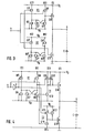
- each of the embodiments contains two preliminary stages V1, V2, each of which consists of a first and a second enhancement load inverter EI1, EI2 or first and second depletion load inverters DI1, DI2, which between the operating voltage V D and the auxiliary voltage V B of opposite polarity are connected.
- the amount of the auxiliary voltage V B is at least equal to the gate blocking voltage (pinch-off voltage) of the depletion end transistors Q10, Q11; in the case of N-channel transistors, it is approximately -3V.
- the enhancement load inverters EI1, EI2 consist of the respective enhancement transistors Q5, Q5 'and the enhancement transistors Q7, Q7' connected to the auxiliary voltage V B.
- the depletion parallel transistors Q6, Q6 ' are connected in parallel, the gates and sources of which are connected to the auxiliary voltage V B.
- the two depletion load inverters DI1, DI2 each consist of the depletion transistors Q8, Q8 'connected to the operating voltage V D and the enhancement transistors Q9, Q9' connected to the source of the auxiliary voltage V B.
- the controlled current paths of the depletion transistors Q8, Q8 'and enhancement transistors Q9, Q9' are connected in series and their common connection point is the buffer inverter output, if necessary.
- Inside and gate of the enhancement transistors Q7, Q9 and Q7 ', Q9' are cross-connected in the manner of a flip-flop, which is controlled by the transistor Q5 and Q5 '.
- the respective output stage ES consists of a depletion end transistor Q10 located at the operating voltage V D and a depletion end transistor Q11 located at the circuit zero, the respective gate of which at the output of the first or of the second depletion load inverter DI1, DI2.
- the two transistors Q10, Q11 are connected in series with their controlled current paths, their common connection point is the output 6 of the buffer inverter, to which the capacitor C, shown in broken lines, is shown as the capacitance mentioned.
- the input 1 is located directly at the gate of the enhancement transistor Q5 of the first enhancement load inverter EI1 and via the inverter 2 at the gate of the enhancement transistor Q5 'of the second enhancement load -Inverter EI2, wherein the gate of depletion transistor Q8 of first depletion load inverter DI1 and the gate of depletion transistor Q8 'of second depletion load inverter DI2 is connected to the associated output.
- input 1 is at the gate of depletion transistor Q8 of the first depletion load inverter DI1 and at the gate of the enhancement transistor Q5 'of the second enhancement load inverter EI2; the gate of the enhancement transistor Q5 of the first enhancement load inverter EI1 is connected to the output of the second depletion load inverter DI2, at which the gate of its depletion transistor Q8 'is also located.
- the inverter 2 according to FIGS. 1 and 2 is missing.
- Fig. 4 shows an embodiment of the buffer inverter which differs not only with respect to the input but also with regard to the final stage and the preliminary stage V2 from the embodiments according to Figs. 1-3.
- the depletion end transistor Q11 of the end stage ES located at the circuit zero is replaced by an enhancement end transistor Q11 '; and the second preliminary stage V2 is replaced by a first driver stage T1 assigned to the depletion end transistor Q10 connected to the operating voltage V D and a second driver stage T2 assigned to the enhancement end transistor Q11 '.
- the first driver stage T1 consists of a third depletion load inverter DI3 located between the operating voltage V D and the auxiliary voltage V B , the depletion transistor Q12 of which has the depletion transistor Q12, the second connected with its gate at the output of the first depletion load inverter DI1: enhancement Parallel transistor Q14 is connected in parallel.
- the gate of the depletion end transistor Q10 is at the output, and the gate of the enhancement transistor Q13 is connected to that of the enhancement transistor Q9 of the first depletion load inverter DI1.
- the second driver stage T2 consists of a fourth depletion load inverter DI4, which lies between the operating voltage V D and the circuit zero point, the depletion transistor Q15 of which is connected to a third enhancement parallel transistor Q17.
- the input 1 of the buffer inverter according to FIG. 4 is directly connected to the gate of the depletion Transistor Q8 of the first depletion load inverter DI1 and that of the enhancement transistor Q16 of the fourth depletion load inverter DI4 connected.
- the input 1 to the gate of the enhancement-mode transistor Q5 of the first enhancement-mode load inverter EI1 and that of the D epletion transistor Q15 and that of the third enhancement-parallel transistor Q17 of the fourth depletion-mode load inverter DI4 respectively.
- a binary signal present at input 1 with the two states H (the more positive of the two binary signal states) or L generally has a signal swing between the potential of the circuit zero point and that of the operating voltage V D. This signal swing is changed by means of the preliminary stage V1 such that it covers the area between the auxiliary voltage V B and the operating voltage V. This is necessary in order to ensure that the depletion end transistor Q10 is safely blocked.
- An H level present at input 1 turns on depletion transistor Q8 so that it reaches its area of good current conduction.
- the conductivity of the enhancement transistor Q5 is reduced by the H level at input 1, which has been converted into an L level by the inverter 2, so that the enhancement load inverter EI has a high-impedance load resistance in this operating state.
- the powerful control of the depletion Transistor Q8 causes it to only a low voltage drops, and thus the output of the first depletion L oad inverter DI1 practically an H level leads.
- enhancement load inverter E I This generates an L level at the output of the enhancement load inverter E I , which in turn keeps the enhancement transistor Q9 blocked, so that this transistor also has an H level at the output of the first depletion load inverter DI1 einfensiv.
- Der enhancement transistor Q5 acts as L astelement the enhancement-load inverter EI, when the e nhancement transistor Q7 is conductive, however, the e-Load nhancement inverter EI as a source follower interacts with the D epletion parallel transistor Q6 as a load element as long as the enhancement transistor Q7 is blocked.
- the driver stage T1 By means of the driver stage T1 it is achieved on the one hand that the L'-level at the output of the first depletion load inverter DI1 is brought even closer to the potential of the auxiliary voltage V and that on the other hand this inverter output is better adapted to the input capacitance of the depletion end transistor Q10 .
- the second depletion load inverter DI2 of the driver stage T1 is controlled via the gate of the enhancement transistor Q13, which is connected to the output of the enhancement load inverter EI1.
- the enhancement parallel transistor Q14 from the output of the first depletion-mode load inverter DI1 is controlled, whereby it is achieved that the switching speed does not deteriorate at low currents in De pletion transistor Q12, that is, when the enhancement transistor Q13 by a L If the level at its gate is blocked and thus only a small current flows in the inverter, the enhancement transistor Q14, which is then conductively controlled by an H level at its gate, charges the gate capacitance of the depletion end transistor Q10.
- the enhancement end transistor Q11 ' is also assigned the driver stage T2, which consists of the third depletion load inverter DI3, the depletion transistor Q15 of which is connected to the second enhancement parallel transistor Q17 and which is connected between the operating voltage V D and the circuit zero is arranged.
- the gate of the enhancement transistor Q17 is connected to that of the depletion transistor Q15 and is driven by input 1 via the inverter .:2.
- the enhancement transistor Q16 of the third depletion load inverter DI3, on the other hand, is driven directly from input 1.
- An H level at input 1 thus causes the enhancement transistor Q16 to turn on while the enhancement parallel transistor Q17 is blocked and a state of low current flow in the depletion transistor Q15.
- the second pre-stage V2 is provided for driving the depletion end transistor Q11 which is at the circuit zero, which, as already explained above, with regard to the type, the number and the interconnection of the individual components with the first pre-stage V1 is identical.
- the three exemplary embodiments according to FIGS. 1 to 3 differ in terms of the control from input 1.
- the inverted and non-inverted form of the input signal in the exemplary embodiment in FIG. 1 serves to control the load transistors Q5, Q5 'of the first and second enhancement load inverters EI1, EI2 and the depletion transistors operated as dynamic load transistors Q8, Q8 '.
- the enhancement transistor Q5 is driven by the non-inverted input signal, the corresponding enhancement transistor Q5 'in the second pre-stage V2, on the other hand, by the inverted input signal, which also drives the depletion transistor Q8 in the pre-stage V1, while the non-inverted input signal drives the depletion transistor Q8 'in the preliminary stage V2.
- FIG. 1 While there is thus complete dynamic control of the load transistors in FIG. 1, in FIG. Contrary to Fig. 1 only provided that the enhancement transistors Q5, Q5 'in the first and second pre-stage V1, V2 are dynamic load elements, while the depletion transistors Q8, Q8' by the aforementioned connection of their gate to the corresponding inverter output are purely resistive load elements.
- FIG. 3 shows a further variant, in which the inverter 2 can be dispensed with, because in the second preliminary stage V2 the depletion transistor Q8 'is a purely resistance-connected load element, the depletion transistor Q8' on the other hand, is a load element dynamically operated by the input signal as is the enhancement transistor Q5 'and because the dynamic activation of the enhancement transistor Q5 takes place from the output of the second depletion load inverter DI2 of the second preliminary stage V2.
- the principle of operation of the two preliminary stages V1, V2 in the exemplary embodiments in FIGS. 1 to 3 is basically the same as that of the first preliminary stage V1 in FIG. 4, as has already been described above. Because of its inverse control, so to speak, the second pre-stage V2 also provides an output signal which is inverse to the output signal of the first pre-stage V1, so that the end stage ES is actually operated in a pure push-pull mode. Since the depletion end transistor Q11 located at the circuit zero point must also be reliably blocked, the second preliminary stage V2 is also arranged between the operating voltage V D and the auxiliary voltage V B , so that the output of the second depletion load inverter DI2 of the second preliminary stage V2 resulting L-level can also safely block this transistor Q11.
Landscapes
- Engineering & Computer Science (AREA)
- Computer Hardware Design (AREA)
- Physics & Mathematics (AREA)
- Computing Systems (AREA)
- General Engineering & Computer Science (AREA)
- Mathematical Physics (AREA)
- Power Engineering (AREA)
- Logic Circuits (AREA)
Abstract
Description
- Die Erfindung betrifft monolithisch mittels Enhancement-und Depletion-Isolierschicht-Feldeffekttransistoren integrierte : Puffer-Inverter nach dem Oberbegriff des Patentanspruchs 1. Derartige Puffer-Inverter sind in der US-PS 3 775 693 beschrieben. Sie eignen sich für die Integration entweder mit P-Kanal-Transistoren oder mit N-Kanal-Transistoren und haben die Eigenschaft, daß der Ausgang praktisch das Potential der Betriebsspannung annimmt, wenn der Enhancement-Transistor sperrt, so daß nur eine Betriebsspannungsquelle erforderlich ist. Ferner bleibt der Strombetrag während des Sperrvorgangs im Depletion-Transistor konstant, so daß sich ein schnelles Schalten ergibt, was immer erwünscht ist, da der Ausgang des Puffer-Inverters an weitere Schaltungsteile angeschlossen ist, die kapazitätsbehaftet sind, d.h. das absichtlich ein Kondensator vorgesehen ist oder daß die Eingangskapazität der Schaltungsteile oder deren Streukapazität nicht vernachlässigbar sind. Schnelles Schalten bedeutet also, daß der Puffer-Inverter diese Kapazität in vorgegebener Zeit auf- und/oder entladen kann.
- Bei einer gegebenen Verlustleistung zeigt die bekannte Schaltung zwar in diesem Sinne günstige Schalteigenschaften, insbesondere bei höheren Betriebsspannungen,sie wird jedoch nicht allen Anforderungen gerecht. Die im Anspruch gekennzeichnete Erfindung löst somit die Aufgabe, einen bezüglich Schaltgeschwindigkeit und/oder Kapazitätsbelastbarkeit verbesserten Puffer-Inverter anzugeben, bei dem der Depletion-Endtransistor sicher gesperrt wird.
- Anhand der Figuren 1 bis 4 der Zeichnung, die Schaltbilder verschiedener Ausführungsformen des Pufferinverters nach der Erfindung darstellen, wird diese nachstehend näher erläutert. In allen Figuren sind die Enhancement-Transistoren mit E und die Depletion-Transistoren mit T zusätzlich zu den übrigen Bezugszeichen markiert.
- In den Fig. 1 bis 3 enthält jede der Ausführungsformen zwei Vorstufen V1, V2, die jeweils aus einem ersten und einem zweiten Enhancement-Load-Inverter EI1, EI2 bzw. ersten und zweiten Depletion-Load-Inverter DI1, DI2 bestehen, die zwischen die Betriebsspannung VD und die Hilfsspannung VB von dazu entgegengesetzter Polarität geschaltet sind. Der Betrag der Hilfsspannung VB ist mindestens jeweils gleich der Gate-Sperrspannung (pinch-off-Spannung) der Depletion-Endtransistoren Q10, Q11; sie beträgt bei N-Kanal-Transistoren somit etwa -3V. Die Enhancement-Load-Inverter EI1, EI2 bestehen aus den jeweiligen Enhancement-Transistoren Q5, Q5' und den an der Hilfsspannung VB liegenden Enhancement-Transistoren Q7, Q7'. Diesen sind die Depletion-Paralleltransistoren Q6, Q6' parallelgeschaltet, deren Gate und Source mit der Hilfsspannung VB verbunden sind.
- Die beiden Depletion-Load-Inverter DI1, DI2 bestehen jeweils aus den an der Betriebsspannung VD liegenden Depletion-Transistoren Q8, Q8' und den mit der Source an der Hilfsspannung VB liegenden Enhancement-Transistoren Q9, Q9'. Die gesteuerten Strompfade der Depletion-Transistoren Q8, Q8' und Enhancement-Transistoren Q9, Q9' sind in Serie geschaltet und ihr gemeinsamer Verbindungspunkt ist ggf. der Puffer-Inverterausgang. Darin und Gate der Enhancement-Transistoren Q7, Q9 bzw. Q7', Q9' sind nach Art eines Flipflops über Kreuz verbunden,das durch den Transistor Q5 bzw. Q5' gesteuert ist. Für die Ausführungsformen nach den Fig. 1 bis 3 gilt darüber hinaus, daß die jeweilige Endstufe ES aus einem an der Betriebsspannung VD liegenden Depletion-Endtransistor Q10 und einem am Schaltungsnullpunkt liegenden Depletion-Endtransistor Q11 besteht, deren jeweiliges Gate am Ausgang des ersten bzw. des zweiten Depletion-Load-Inverters DI1, DI2 liegt. Die beiden Transistoren Q10, Q11 sind mit ihren gesteuerten Strompfaden in Serie geschaltet, ihr gemeinsamer Verbindungspunkt ist der Ausgang 6 des Puffer-Inverters, an den angeschlossen der gestrichelt gezeichnete Kondensator C als die erwähnte Kapazität gezeigt ist.
- Abweichend von diesen Gemeinsamkeiten liegt bei der Ausführungsform nach Fig. 1 der Eingang 1 des Puffer-Inverters direkt an dem Gate des Enhancement-Transistors Q5 des ersten Enhancement-Load-Inverters EI.und dem des Depletion-Transistors Q8' des zweiten Depletion-Load-Inverters DI2 sowie über einen Inverter 2 an dem Gate des Enhancement-Transistors Q5' des zweiten Enhancement-Load-Inverters EI2 und dem des Depletion-Transistors Q8 des ersten Depletion-Load-Inverters DI1.
- Bei der in Fig. 2 dargestellten Ausführungsform des Puffer- Inverters liegt der Eingang 1 direkt am Gate des Enhancement-Transistors Q5 des ersten Enhancement-Load-Inverters EI1 und über den Inverter 2 am Gate des Enhancement-Transistors Q5' des zweiten Enhancement-Load-Inverters EI2, wobei das Gate des Depletion-Transistors Q8 des ersten Depletion-Load-Inverters DI1 und das Gate des Depletion-Transistors Q8' des zweiten Depletion-Load-Inverters DI2 mit dem zugehörigen Ausgang verbunden ist.
- In der Ausführungsform eines Inverter-Puffers nach Fig. 3 liegt der Eingang 1 am Gate des Depletion-Transistors Q8 des ersten Depletion-Load-Inverters DI1 und am Gate des Enhancement-Transistors Q5' des zweiten Enhancement-Load-Inverters EI2; dabei ist das Gate des Enhancement-Transistors Q5 des ersten Enhancement-Load-Inverters EI1 an den Ausgang des zweiten Depletion-Load-Inverters DI2 angeschlossen, an dem auch das Gate seines Depletion-Transistors Q8' liegt. Der Inverter 2 nach Fig. 1 und 2 fehlt.
- Fig. 4 zeigt eine Ausführungsform des Puffer-Inverters die sich nicht nur bezüglich des Einganges sondern auch bezüglich der Endstufe und der Vorstufe V2von den Ausbildungsformen nach den Fig. 1 bis 3 unterscheidet. So ist in ihr der am Schaltungsnullpunkt liegende Depletion-Endtransistor Q11 der Endstufe ES durch einen Enhancement-Endtransistor Q11' ersetzt; und die zweite Vorstufe V2 ist durch eine dem an der Betriebsspannung VD liegenden Depletion-Endtransistor Q10 zugeordnete erste Treiberstufe T1 und eine dem Enhancement-Endtransistor Q11' zugeordnete zweite Treiberstufe T2 ersetzt. Dabei besteht die erste Treiberstufe T1 aus einem zwischen der Betriebsspannung VD und der Hilfsspannung VB liegenden dritten Depletion-Load-Inverter DI3, dessen Depletion-Transistor Q12 der mit seinem Gate am Ausgang des ersten Depletion-Load-Inverters DI1 angeschlossene zweite: Enhancement-Paralleltransistor Q14 parallelgeschaltet ist. Das Gate des Depletion-Endtransistors Q10 liegt am Ausgang,und das Gate des Enhancement-Transistors Q13 ist mit dem des Enhancement-Transistors Q9 des ersten Depletion-Load-Inverters DI1 verbunden. Die zweite Treiberstufe T2 besteht aus einem zwischen der Betriebsspannung VD und dem Schaltungsnullpunkt liegenden vierten Depletion-Load-Inverter DI4, dessen Depletion-Transistor Q15 ein dritter Enhan-Pement-Paralleltransistor Q17 parallelgeschaltet ist. Der Eingang 1 des Puffer-Inverters nach Fig. 4 ist direkt mit dem Gate des Depletion-Transistors Q8 des ersten Depletion-Load-Inverters DI1 und dem des Enhancement-Transistors Q16 des vierten Depletion-Load-Inverters DI4 verbunden. Über den Inverter 2 ist der Eingang 1 mit dem Gate des Enhancement-Transistors Q5 des ersten Enhancement-Load-Inverters EI1 und dem des Depletion-Transistors Q15 sowie dem des dritten Enhancement-Paralleltransistors Q17 des vierten Depletion-Load-Inverters DI4 verbunden.
- Zur folgenden Erläuterung der Funktionsweise der in den Figuren 1 bis 4 gezeigten Ausbildungsbeispielen ist vorausgesetzt, daß diese mit positiver Logik arbeiten und aus N-Kanal-Transistoren bestehen, d.h. daß die Betriebsspannung VD positiv und die Hilfsspannung V negativ ist.
- Zunächst wird die Funktionsweise des Ausbildungsbeispiels nach Fig. 4 erläutert. Ein am Eingang 1 anliegendes Binärsignal mit den beiden Zuständen H (der positivere der beiden Binärsignalzustände) bzw. L hat im allgemeinen einen Signalswing zwischen dem Potential des Schaltungsnullpunkts und dem der Betriebsspannung VD. Mittels der Vorstufe V1 wird dieser Signalswing so verändert, daß er den Bereich zwischen der Hilfsspannung VB und der Betriebsspannung V abdeckt. Dies ist erforderlich, um ein sicheres Sperren des Depletion-Endtransistors Q10 sicherzustellen. Ein am Eingang 1 anliegender H-Pegel steuert den Depletion-Transistor Q8 auf, so daß dieser in seinen Bereich guter Stromführung gelangt. Andererseits wird die Leitfähigkeit des Enhancement-Transistor Q5 durch den über den Inverter 2 in einen L-Pegel verwandelten H-Pegel am Eingang 1 herabgesetzt, so daß der Enhancement-Load-Inverter EI in diesem Betriebszustand einen hochohmigen Arbeitswiderstand aufweist. Das kräftige Durchsteuern des Depletion-Transistors Q8 führt dazu, daß an ihm nur eine geringe Spannung abfällt und somit der Ausgang des ersten Depletion- Load-Inverter DI1 praktisch einen H-Pegel führt. Dieser erzeugt am Ausgang des Enhancement-Load-Inverters EI einen L-Pegel, der wiederum den Enhancement-Transistor Q9 gesperrt hält, so daß auch von diesem Transistor aus sich am Ausgang des ersten Depletion-Load-Inverters DI1 etwa ein H-Pegel einstellt.Der Enhancement-Transistor Q5 wirkt als Lastelement des Enhancement-Load-Inverter EI, wenn der Enhancement-Transistor Q7 leitend ist, dagegen wirkt der Enhancement-Load-Inverter EI als Source-Folger mit dem Depletion-Paralleltransistor Q6 als Lastelement solange der Enhancement-Transistor Q7 gesperrt ist.
- ;Am Ausgang des ersten Depletion-Load-Inverters DI1 tritt somit ein Signalswing auf, dessen H-Pegel praktisch mit dem des Eingangssignals identisch ist, während dessen L-Pegel, im folgenden mit L' bezeichnet, niedriger als das Potential des Schaltungsnullpunkts liegt. Mit diesem Signalswing wird der Depletion-Endtransistor Q10 über die Treiberstufe T1 angesteuert. Dadurch wird erreicht, daß dieser Transistor sicher vom L'-Pegel gesperrt wird und sich bezüglich der Endstufe ES somit ein möglichst ideales Gegentaktverhalten ergibt, was;mit dem Eingangssignal L-Pegel nicht der Fall wäre.
- Mittels der Treiberstufe T1 wird einerseits erreicht, daß der L'-Pegel am Ausgang des ersten Depletion-Load-Inverters DI1 noch näher an das Potential der Hilfsspannung V gebracht wird und daß andererseits dieser Inverterausgang besser an die Eingangskapazität des Depletion-Endtransistors Q10 angepaßt ist. Die Steuerung des zweiten Depletion-Load-Inverters DI2 der Treiberstufe T1 erfolgt über das Gate des Enhancement-Transistors Q13, das mit dem Ausgang des Enhancement-Load-Inverters EI1 verbunden ist. Andererseits ist der Enhancement-Paralleltransistor Q14 vom Ausgang des ersten Depletion-Load-Inverters DI1 gesteuert, wodurch erreicht wird, daß bei niedrigen Strömen im Depletion-Transistor Q12 die Schaltgeschwindigkeit sich nicht verschlechtert, d.h., wenn der Enhancement-Transistor Q13 durch einen L-Pegel an seinem Gate gesperrt wird und somit im Inverter nur ein geringer Strom fließt, übernimmt der dann durch einen H-Pegel an seinem Gate gerade leitend gesteuerte Enhancement-Transistor Q14 die Aufladung der Gate-Kapazität des Depletion-Endtransistors Q10.
- In vergleichbarer Weise ist auch dem Enhancement-Endtransistor Q11' die Treiberstufe T2 zugeordnet, die aus dem dritten Depletion-Load-Inverter DI3 besteht, dessen Depletion-Transistor Q15 der zweite Enhancement-Parallel- transistor Q17 parallelgeschaltet ist und der zwischen der Betriebsspannung VD und dem Schaltungsnullpunkt angeordnet ist. Das Gate des Enhancement-Transistors Q17 ist mit dem des Depletion-Transistors Q15 verbunden und wird vom Eingang 1 über den Inverter.:2 angesteuert. Der Enhancement-Transistor Q16 des dritten Depletion-Load-Inverters DI3 wird dagegen direkt vom Eingang 1 aus angesteuert. Somit bewirkt ein H-Pegel am Eingang 1 das Durchsteuern des Enhancement-Transistors Q16 bei gleichzeitigem Sperren des Enhancement-Paralleltransistors Q17 und einen Zustand geringer Stromführung im Depletion-Transistor Q15. Dadurch wird am Ausgang des dritten Depletion-Load-Inverters DI3 ein sehr niedriger L-Pegel erzeugt, der den Enhancement-Endtransistor Q11' sicher sperrt. Bei einem L-Pegel am Eingang des Enhancement-Transistors Q16 dagegen werden die Transistoren Q15, Q17 stark durchgesteuert, so daß am Ausgang des dritten Depletion-Load-Inverters DI3 ein praktisch mit der Betriebsspannung V identischer H-Pegel auftritt, der den Enhancement-Endtransistor Q11' sicher durchsteuert.
- In den Ausführungsbeispielen der Figuren 1 bis 3 ist zur Ansteuerung des am Schaltungsnullpunkt liegenden Depletion-Endtransistors Q11 jeweils die zweite Vorstufe V2 vorgesehen, die, wie oben bereits dargelegt wurde, bezüglich der Art, der Anzahl und der Zusammenschaltung der einzelnen Bauelemente mit der ersten Vorstufe V1 identisch ist. Die drei Ausführungsbeispiele nach den Figuren 1 bis 3 unterscheiden sich hinsichtlich der Ansteuerung vom Eingang 1 aus. So dient das Eingangssignal beim Ausführungsbeispiel der Figur 1 in seiner invertierten und seiner nichtinvertierten Form zur Ansteuerung der Last-Transistoren Q5, Q5' des ersten und des zweiten Enhancement-Load-Inverters EI1, EI2 und der als dynamische Last-Transistoren betriebenen Depletion-Transistoren Q8, Q8'. In der ersten Vorstufe V1 wird der Enhancement-Transistor Q5 vom nichtinvertierten Eingangssignal, der entsprechende Enhancement-Transistor Q5' in der zweiten Vorstufe V2 dagegen vom invertierten Eingangssignal angesteuert, das auch den Depletion-Transistor Q8 in der Vorstufe V1 ansteuert, während das nichtinvertierte Eingangssignal in der Vorstufe V2 den Depletion-Transistor Q8' ansteuert.
- Während in Fig. 1 somit eine vollständige dynamische Steuerung der Lasttransistoren vorliegt, ist in Fig. 2 im . Gegensatz zur Fig. 1 nur vorgesehen, daß die Enhancement-Transistoren Q5, Q5' in der ersten bzw. zweiten Vorstufe V1, V2 dynamische Lastelemente sind, während die Depletion-Transistoren Q8, Q8' durch die erwähnte Verbindung ihres Gates mit dem entsprechenden Inverterausgang rein widerstandsgeschaltete Lastelemente sind.
- Die Figur 3 zeigt eine weitere Variante, bei der auf den Inverter 2 verzichtet werden kann, weil in der zweiten Vorstufe V2 der Depletion-Transistor Q8' ein rein widerstandsgeschaltetes Lastelement ist, der Depletion-Transistor Q8' dagegen ein vom Eingangssignal dynamisch betriebenes Lastelement ebenso wie der Enhancement-Transistor Q5' ist und weil die dynamische Ansteuerung des Enhancement-Transistors Q5 vom Ausgang des zweiten Depletion-Load-Inverters DI2 der zweiten Vorstufe V2 aus erfolgt.
- Die Wirkungsweise der beiden Vorstufen V1, V2 in den Ausführungsbeispielen der Figuren 1 bis 3 ist dem Prinzip nach dieselbe wie die der ersten Vorstufe V1 in Fig. 4, wie sie oben bereits beschrieben worden ist. Die zweite Vorstufe V2 liefert wegen ihrer sozusagen inversen Ansteuerung an ihrem Ausgang auch ein zum Ausgangssignal der ersten Vorstufe V1 inverses Ausgangssignal, so daß die Endstufe ES tatsächlich in reinem Gegentakt betrieben wird. Da der am Schaltungsnullpunkt liegende Depletion-Endtransistor Q11 ebenfalls sicher gesperrt werden muß, ist die zweite Vorstufe V2 ebenfalls zwischen der Betriebsspannung VD und der Hilfsspannung VB angeordnet, so daß der am Ausgang des zweiten Depletion-Load-Inverters DI2 der zweiten Vorstufe V2 entstehende L'-Pegel auch diesen Transistor Q11 sicher sperren kann.
Claims (2)
Applications Claiming Priority (4)
| Application Number | Priority Date | Filing Date | Title |
|---|---|---|---|
| US213533 | 1980-12-05 | ||
| US06/213,533 US4395645A (en) | 1980-12-05 | 1980-12-05 | Mosfet logic inverter buffer circuit for integrated circuits |
| DE3146485 | 1981-11-24 | ||
| DE19813146485 DE3146485A1 (de) | 1981-11-24 | 1981-11-24 | "monolithisch integrierter puffer-inverter" |
Publications (3)
| Publication Number | Publication Date |
|---|---|
| EP0053798A2 true EP0053798A2 (de) | 1982-06-16 |
| EP0053798A3 EP0053798A3 (en) | 1983-01-05 |
| EP0053798B1 EP0053798B1 (de) | 1985-08-28 |
Family
ID=25797523
Family Applications (1)
| Application Number | Title | Priority Date | Filing Date |
|---|---|---|---|
| EP81110096A Expired EP0053798B1 (de) | 1980-12-05 | 1981-12-03 | Monolithisch integrierter Puffer-Inverter |
Country Status (2)
| Country | Link |
|---|---|
| EP (1) | EP0053798B1 (de) |
| DE (1) | DE3172081D1 (de) |
Cited By (1)
| Publication number | Priority date | Publication date | Assignee | Title |
|---|---|---|---|---|
| EP0141474A3 (en) * | 1983-11-08 | 1985-07-10 | N.V. Philips' Gloeilampenfabrieken | Digital signal switching circuit |
Family Cites Families (2)
| Publication number | Priority date | Publication date | Assignee | Title |
|---|---|---|---|---|
| US3775693A (en) * | 1971-11-29 | 1973-11-27 | Moskek Co | Mosfet logic inverter for integrated circuits |
| JPS5198938A (de) * | 1975-02-26 | 1976-08-31 |
-
1981
- 1981-12-03 EP EP81110096A patent/EP0053798B1/de not_active Expired
- 1981-12-03 DE DE8181110096T patent/DE3172081D1/de not_active Expired
Cited By (1)
| Publication number | Priority date | Publication date | Assignee | Title |
|---|---|---|---|---|
| EP0141474A3 (en) * | 1983-11-08 | 1985-07-10 | N.V. Philips' Gloeilampenfabrieken | Digital signal switching circuit |
Also Published As
| Publication number | Publication date |
|---|---|
| DE3172081D1 (en) | 1985-10-03 |
| EP0053798B1 (de) | 1985-08-28 |
| EP0053798A3 (en) | 1983-01-05 |
Similar Documents
| Publication | Publication Date | Title |
|---|---|---|
| DE3228013C2 (de) | Bidirektionale Sammelleitung zum Datentransfer | |
| DE2721851A1 (de) | Verriegelnder leseverstaerker fuer halbleiterspeicheranordnungen | |
| DE2625007B2 (de) | Adressenpufferschaltung für Halbleiterspeicher | |
| EP0044066A2 (de) | Treiberstufe in integrierter MOS-Schaltkreistechnik mit grossem Ausgangssignalverhältnis | |
| DE69218746T2 (de) | Einschalt-Rücksetzschaltung | |
| DE19751789A1 (de) | Spannungspegel-Verschiebeschaltung | |
| DE19743298C2 (de) | Impulsformerschaltung | |
| DE2835692B2 (de) | Binäres logisches ODER-Glied für programmierte logische Anordnungen | |
| DE69013498T2 (de) | Komplementäre feldeffekt-transistorlogik mit hoher geschwindigkeit. | |
| DE3741913C2 (de) | CMOS-Logikschaltung | |
| DE3108342A1 (de) | Dynamische schieberegisterschaltung | |
| DE2842690A1 (de) | Mos-festwertspeicher | |
| DE2435454A1 (de) | Dynamischer binaerzaehler | |
| EP0053798B1 (de) | Monolithisch integrierter Puffer-Inverter | |
| DE19637013A1 (de) | Treiberschaltung | |
| DE2165160C2 (de) | CMOS-Schaltung als exklusives ODER-Glied | |
| EP0905892B1 (de) | RS-Flip-Flop mit Enable-Eingängen | |
| EP0065022A1 (de) | Integrierter Spannungsteiler mit Auswahlschaltung in Isolierschicht-Feldeffekttransistor-Technik, dessen Abwandlung und seine Verwendung in einem Digital-Analog-Wandler | |
| EP0024549A1 (de) | TTL-Pegelumsetzer zur Ansteuerung von Feldeffekttransistoren | |
| DE3037132A1 (de) | Schaltungsanordnung zur schnellen weitergabe von binaersignalen | |
| EP0015364B1 (de) | Multivibrator aus Feldeffekt-Transistoren | |
| DE2355408A1 (de) | Logische schaltung | |
| DE2448099A1 (de) | Dekodierschaltung mit komplementaeren feldeffekttransistoren | |
| EP0055795B1 (de) | Schnelle MOS-Treiberschaltung für Digitalsignale | |
| DE2901234A1 (de) | Zweizustandsschaltung |
Legal Events
| Date | Code | Title | Description |
|---|---|---|---|
| PUAI | Public reference made under article 153(3) epc to a published international application that has entered the european phase |
Free format text: ORIGINAL CODE: 0009012 |
|
| AK | Designated contracting states |
Designated state(s): DE FR GB IT NL |
|
| PUAL | Search report despatched |
Free format text: ORIGINAL CODE: 0009013 |
|
| AK | Designated contracting states |
Designated state(s): DE FR GB IT NL |
|
| 17P | Request for examination filed |
Effective date: 19830614 |
|
| ITF | It: translation for a ep patent filed | ||
| GRAA | (expected) grant |
Free format text: ORIGINAL CODE: 0009210 |
|
| AK | Designated contracting states |
Designated state(s): DE FR GB IT NL |
|
| REF | Corresponds to: |
Ref document number: 3172081 Country of ref document: DE Date of ref document: 19851003 |
|
| ET | Fr: translation filed | ||
| PLBE | No opposition filed within time limit |
Free format text: ORIGINAL CODE: 0009261 |
|
| STAA | Information on the status of an ep patent application or granted ep patent |
Free format text: STATUS: NO OPPOSITION FILED WITHIN TIME LIMIT |
|
| 26N | No opposition filed | ||
| PGFP | Annual fee paid to national office [announced via postgrant information from national office to epo] |
Ref country code: NL Payment date: 19861231 Year of fee payment: 6 |
|
| PG25 | Lapsed in a contracting state [announced via postgrant information from national office to epo] |
Ref country code: NL Effective date: 19880701 |
|
| NLV4 | Nl: lapsed or anulled due to non-payment of the annual fee | ||
| GBPC | Gb: european patent ceased through non-payment of renewal fee | ||
| PG25 | Lapsed in a contracting state [announced via postgrant information from national office to epo] |
Ref country code: FR Free format text: LAPSE BECAUSE OF NON-PAYMENT OF DUE FEES Effective date: 19880831 |
|
| PG25 | Lapsed in a contracting state [announced via postgrant information from national office to epo] |
Ref country code: DE Effective date: 19880901 |
|
| REG | Reference to a national code |
Ref country code: FR Ref legal event code: ST |
|
| PG25 | Lapsed in a contracting state [announced via postgrant information from national office to epo] |
Ref country code: GB Free format text: LAPSE BECAUSE OF NON-PAYMENT OF DUE FEES Effective date: 19881118 |