EP0053935B1 - Verfahren und Apparat zur Änderung falscher Datenelemente in digitalen Bildern - Google Patents
Verfahren und Apparat zur Änderung falscher Datenelemente in digitalen Bildern Download PDFInfo
- Publication number
- EP0053935B1 EP0053935B1 EP81305763A EP81305763A EP0053935B1 EP 0053935 B1 EP0053935 B1 EP 0053935B1 EP 81305763 A EP81305763 A EP 81305763A EP 81305763 A EP81305763 A EP 81305763A EP 0053935 B1 EP0053935 B1 EP 0053935B1
- Authority
- EP
- European Patent Office
- Prior art keywords
- data elements
- pixel
- erroneous
- masks
- data
- Prior art date
- Legal status (The legal status is an assumption and is not a legal conclusion. Google has not performed a legal analysis and makes no representation as to the accuracy of the status listed.)
- Expired
Links
Images






Classifications
-
- G—PHYSICS
- G06—COMPUTING OR CALCULATING; COUNTING
- G06T—IMAGE DATA PROCESSING OR GENERATION, IN GENERAL
- G06T5/00—Image enhancement or restoration
- G06T5/20—Image enhancement or restoration using local operators
-
- H—ELECTRICITY
- H04—ELECTRIC COMMUNICATION TECHNIQUE
- H04N—PICTORIAL COMMUNICATION, e.g. TELEVISION
- H04N1/00—Scanning, transmission or reproduction of documents or the like, e.g. facsimile transmission; Details thereof
- H04N1/40—Picture signal circuits
- H04N1/409—Edge or detail enhancement; Noise or error suppression
-
- H—ELECTRICITY
- H04—ELECTRIC COMMUNICATION TECHNIQUE
- H04N—PICTORIAL COMMUNICATION, e.g. TELEVISION
- H04N1/00—Scanning, transmission or reproduction of documents or the like, e.g. facsimile transmission; Details thereof
- H04N1/40—Picture signal circuits
- H04N1/409—Edge or detail enhancement; Noise or error suppression
- H04N1/4097—Removing errors due external factors, e.g. dust, scratches
Definitions
- This invention relates to a method and apparatus for altering erroneous data elements in digital images generated during the scanning of a document.
- a digital image is formed with each picture element having a colour value of one of a multi-value colour scale (which may range from white to black through different shades of grey).
- a colour value of one of a multi-value colour scale which may range from white to black through different shades of grey.
- it is normal to reduce the values of the colour scale to two values, black and white, so that each picture element has one of only two values. This process of simplifying the image is known as thresholding.
- noise When generating thresholded black and white facsimile images, electronic noise is often generated. Such noise is exhibited as holes or white spots in the middle of dark areas of a figure, single or small groups of black dots in white areas of an image, or unsmooth edges of figures. Noise increases the number of bits which must be transmitted to form a facsimile image. The noise itself does not contain any useful information; thus, by suppressing this noise, visual and machine pattern recognition are greatly aided. Furthermore, noise reduction improves data compression performance, since it improves the line-to-line correlation in its facsimile image, which is the basis of many compression methods. This improves correlation and also results in faster data transmission.
- U.S. Patent No. 3 700 797 discloses a method of reducing noise in digital images by deleting groups of pulses of less than a predetermined number in each scanned row of the image.
- this method is relatively elementary and cannot deal with all possible situations such as row edges and the blacking of holes or white spots in dark areas of a figure.
- U.S. Patent No. 3 624006 discloses a method of reducing noise in digital images by validating the direction of lines in the image and eliminating parts of the image not forming part of the validated image and hence due to noise.
- Such method is not suitable for images which cannot be represented as a series of straight lines.
- a "faulty" polyomino is a polyomino pattern in which, except for the "end" squares, one. or more of the squares making up the polyomino may be omitted.
- the present invention provides an apparatus for altering erroneous data elements generated during the scanning of a document to produce a digital image, including first means for receiving a plurality of data elements obtained by scanning said document, characterized in. that said first means includes storage means for storing a specific number of said data elements at any particular time, and further characterized by second means coupled to said first means for determining whether any of said data elements stored within said first means are erroneous and should be altered, said second means including multiple logic masks contained in a field programmable logic array, said multiple logic masks being arranged to be applied simultaneously to selectively test said stored data elements for errors, third means, coupled to said first and second means, for altering any data elements which are deemed to be erroneous by said second means, and control means, coupled to said first means, for generating a plurality of control signals for use in controlling the transfer of said data elements into and out of said first means.
- the present invention provides a method of altering erroneous data elements generated by a document scanning operation to produce a digital image, characterized by the steps of: a) receiving a single data element from a plurality of data elements generated by said scanning operation and storing said data element into a storage means, which may contain a specific number of data elements stored in a pre-defined pattern at any particular time; b) repeating step a) a sufficient number of times to load said storage means with the desired number of data elements to provide said pattern; c) examining the data elements stored in said pre-defined pattern by a simultaneous comparison of the data elements stored in said pattern with each of multiple logic masks contained in a field programmable logic array device to determine whether any of the data elements stored in said pattern are erroneous and should be altered; d) altering any data elements which have been deemed to be erroneous by logically combining said erroneous element with an associated control signal from said field programmable logic array device to reverse the state of said er
- FIG. 1 A simplified block diagram of the noise cleaner of the present invention is shown in Fig. 1.
- a stream of pixels is transmitted serially to a window memory unit 10.
- Unit 10 forms the 5 x 5 pixel matrix used to examine the facsimile data for unwanted noise pixels. This twenty-five pixel matrix is transmitted to a mask logic unit 12.
- Unit 12 compares the matrix pixels to a series of masks, and determines which pixels, if any, should be altered to remove noise from the facsimile image. In the present embodiment, it has been determined that it is necessary to alter only the contents of two particular pixel positions at any time to remove unwanted pixels, as will subsequently be shown.
- the altered pixels are then transmitted back to window memory unit 10 to replace the corresponding original pixels in the pixel matrix.
- Unit 10 serially outputs a stream of cleaned pixels which is transmitted to a data compression. unit (not shown) for transmission of the facsimile image.
- a timing and control unit 14 regulates the operation of window memory unit 10.
- window memory unit 10 The structure of window memory unit 10 is shown in Fig. 2, in which the 5x5 pixel matrix which comprises the window memory unit 10 is shown in a more detailed block diagram.
- the twenty-five pixels, which are labelled Al-A5 through El-E5 inclusive, are shown as they appear on the original image with respect to the direction of scanning by the image lift unit (not shown) and the direction of document travel.
- A1 is the newest pixel entering the matrix
- E5 is the oldest pixel contained.
- each line contains 640 pixels; however, the hardware may be manipulated to accommodate any size documents.
- Each pixel enters the matrix at the A1 position and is propagated through the A2, A3, A4, and A5 positions, as shown in Fig. 3. From the A5 position, the bit is clocked into a shift register 30, containing 636 bits, the last bit of which constitutes the B1 position in the matrix.
- This shift register causes a one line delay of the pixel, so that as each pixel moves through the matrix, its relative position to other pixels in the real image remains the same. From the B1 position, the pixel is clocked through B2, B3, B4 and B5 positions, and into a shift register 32, a 636 bit device, the last bit of which constitutes the C1 position.
- This pixel continues through positions Cl-C5, shift register 34, positions Dl-D5, and shift register 36 in the same manner as previously described.
- the pixel is outputted from position E1, which is the last bit of shift register 36, the pixel is outputted to the compression hardware, and is also transmitted to position E2, to be used in the matrix. From position E2, the pixel propagates through E3, E4, and E5, which position is the last in the matrix.
- the 25 pixel positions of the 5x5 matrix of Fig. 3 are applied in parallel to the inputs of an FPLA array which has been programmed to compare each input window pattern against a set of masks to determine how the pixels in the window should be altered to suppress noise.
- the contents of each window pattern is compared to all masks simultaneously by the FPLA array, which outputs signals to alter any pixels which are deemed to be erroneous.
- the masks can be classified as to their function: (1) to remove single isolated points (2) to remove two isolated points of any rotation; (3) to remove three isolated points of rotation; (4) line edge cleaning; (5) line edge filling; (6) corner enhancement; and (7) special cases.
- special cases of double hole filling and character reconstruction may be accommodated.
- 10 basic mask types are used to cover all cases except special cases and unit pixel removal. There are four rotations of each mask, necessitating 40 different masks. In addition, there are two fundamental masks to remove or set a discrete bit, for a final total of 42 masks.
- pixel matrix of window memory unit 10 (Fig. 1) is actually arranged according to Fig. 2, the matrix is considered to be conventionally labelled as shown in Fig. 4 for convenience. This conventional change must be remembered when analyzing the unit function or special masks of only one orientation when coded into the FPLAs.
- Fig. 5 displays the different symbols used in interpreting the mask set of the preferred embodiment.
- symbol 40 represents a dark or "active" pixel in each of the masks.
- Symbol 42 represents a dark pixel which is to be inverted to a light pixel, while symbol 44 represents a light pixel which is to be inverted to a dark pixel.
- Symbol 46 represents a condition where it is immaterial whether the pixel is light or dark, a "don't care" condition.
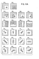
- Figs. 6A & B, inclusive depict the set of masks contained in the mask logic 12 (Fig. 1) which were developed for the present embodiment. It should be noted that this set of masks was derived experimentally for use on a certain type of two dimensional digital images (checks). Other types of image patterns could be better serviced by a different set of masks, or further experimentation may provide a different set which exhibits improved compression performance.
- masks 50 and 52 are fundamental masks used for isolated unit pixel removal and addition.
- Mask 50 operates to remove a single dark pixel from a light area of the image.
- Mask 52 fills a hole created by a missing pixel in the centre of a dark area on the image.
- Masks 54 through 68, inclusive perform edge cleaning functions upon the characters contained in digital images.
- Mask 54 through 60, inclusive operate to remove an unwanted pixel from the edge of pixel group, while masks 62 through 68, inclusive, insert a missing pixel into a group of pixels.
- Masks 70 through 76, inclusive act upon isolated two pixel groups of noise, while masks 78 through 116, inclusive, perform pixel removal in cases involving isolated three pixel groups of various orientations.
- Masks 118 through 132, inclusive involve corner enhancing operations, with masks 118 through 124, inclusive, acting to remove an extra pixel on an inside corner of a figure, while masks 126 through 132, inclusive, add a missing pixel to an outside corner of a figure.
- Fig. 7 shows several examples of the operation of the mask set contained in the mask logic 12 (Fig. 2) of the present embodiment in the removal of noise.
- a three pixel group representing noise is shown at frame 150a.
- the pixel group moves to the position shown in frame 150b when the next pixel enters the matrix.
- mask 106 (Fig. 6B) removes the pixel at position C3 in the matrix.
- the pixel group (now containing only two pixels) is again shifted one line downward to the position shown in Frame 150c.
- the pixel at position C3 in the matrix is removed.
- the final pixel remaining in the three pixel group is removed in position D4 by applying mask 50 (Fig. 6A) to the matrix.
- Frame 1 52a shows a different three pixel configuration (representing noise) in the window matrix of unit 10 (Fig. 1).
- the configuration is shifted downward one line in the matrix to the position shown in frame 152b, allowing one pixel to be removed at position C3 using mask 96 (Fig. 6B).
- the two remaining pixels are shifted downward one line to the position shown in frame 152c, and, using mask 50 (Fig. 6A), the pixel at position D4 is removed.
- the remaining pixel arrives at the position D4 shown in frame 152d (after 1281 additional pixels have entered the matrix), it is removed by mask 50 (Fig. 6A), and the three pixel group is thus completely eliminated from the image.
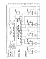
- Figs. 8A-C shows in detail the logic circuitry for the window memory unit 10 shown in Fig. 1.
- the 5x5 matrix is comprised of an array of D-type flip-flops, 1 60a-e through 168a-e, inclusive, which are arranged to simulate the matrix window.
- the output of each of the twenty-five flip-flops, which output is represented by hexagons Al-A5 through El-E5, inclusive, is tapped and outputted to the mask logic circuitry 12 (Fig. 1).
- Matrix window position C3, which is the output of flip-flop 164c, is combined with a data bit C3', which represents a "cleaned” pixel outputted from the mask logic circuitry 12, via an EXCLUSIVE OR gate 169.
- the output of gate 169 is transmitted to flip-flop 166c.
- matrix window position D4, which is the output of flip-flop 166d, is combined with data bit D4', representing another "cleaned” data bit from the mask logic, via an EXCLUSIVE OR gate 170.
- the output of gate 170 is transmitted to flip-flop 168d.
- Gates 169 and 170 operate to update the window matrix with corrected pixels.
- a logic 1 outputted from the mask logic operates to invert the original data pixel, causing a blank to become a dot or a dot to become a blank on digitized image.
- Flip-flops 160a-e inclusive which together form the top line of the 5x5 matrix window, each receive an input from a bidirectional driver 171, which may be a 8T26A integrated circuit chip manufactured by Signetics, or an equivalent device.
- a fixed count length synchronous counter 172 provides addressing to a 1024x4 bit random access memory (RAM) chip 174 for simulating a set of four 636 bit shift registers, as is shown in Fig. 3.
- RAM random access memory
- chip 174 is a 2114-4 Random Access Memory chip manufactured by Intel Corp, or an equivalent device.
- a count of 635 is decoded by counter 172 and enables a synchronous loading to zero on the next clock pulse, which total 636 counts.
- the output data from counter 172 which comprises a 10 bit address bus 176, addresses RAM 174, transmitting the corresponding RAM output to flip-flops 160b-e via driver 171.
- Flip-flops 1 60a-e are clocked by a signal RL, while flip-flops 162a-e through 168a-e, inclusive, are clocked by a signal UMS. The generation of these signals will be described in detail subsequently.
- Signal UMS also is transmitted to the write enable port of RAM 174, and to the data in enable port of driver 171 via an inverter 180. In operation, the data is clocked through the window matrix formed by flip-flops 160a through 168e, inclusive, in the manner shown in Fig. 3.
- the pixel is transmitted to a flip-flop 182, which flip-flop is clocked by a signal DVO.
- the output of flip-flop 182 is inverted by an inverter 184 to generate a DATA OUT signal. This signal is then transmitted to the data compression hardware (not shown).
- Signal DVO is transmitted to an inverter 186 to generate a DAVLIDOUT signal.
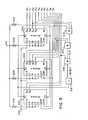
- counter 172 is comprised of synchronous binary counters 200, 202, 204, which may be of the type 74LS161A manufactured by Texas Instruments, or an equivalent device.
- the data inputs ports A, B, C and D of counter 200 are connected to the supply voltage V cc via a resistor 206, as are both enable inputs ENT and ENP.
- Data output ports Q A , Q B , Q C and O D are connected respectively to the A o , A 1 , A 2 , and A3 lines of the address bus 176.
- the ripple carry output RC of counter 200 is connected to the enable inputs ENT and ENP of counter 202, and also to the enable input ENT of counter 204.
- the data input ports A, B, C and D of counter 202 are connected to supply voltage V CC via a resistor 208, while the data output ports are connected respectively to the A4, A 5 , A 6 and A 7 lines of address bus 176.
- the ripple carry output RC of counter 202 is connected to enable input ENP of counter 204.
- the data input ports A, B, C and D of counter 204 are connected to the supply voltage V CC via resistor 210, While the data output ports O A and Q B are connected respectively to address lines A a and Ag of address bus 176.
- the load input LD of counters 202, 203, and 204 are all connected to supply voltage V CC via a resistor 212, while the counters are all clocked by the signal DVO.
- Address lines A 2 , A3, and A4 are combined by an AND gate 214, while the output of gate 214 is combined with address lines A 5 and A 6 via an AND gate 216.
- the output of gate 216 is combined with address line Ag via an AND gate 218.
- the output of gate 218 is connected through an OR gate 219, to which a RESET signal is also applied, to the clear inputs CL of counters 200, 202, and 204.
- each pulse of DVO increments counter 172 once, causing its output, which is address bus 176, to address RAM 174.
- address lines A 2 , A3, A4, A 5 , A 6 and Ag are active, enabling gates 214, 216, 218, and 219, clearing registers 200, 202, and 204, and resetting counter 172 to zero.
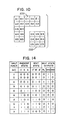
- the matrix contained in window memory unit 10 is split into two sub-masks, 220 and 222, as shown in Fig. 10, with one sub-mask forming an input for the other.
- Sub-mask 220 also designated as FPLA1
- sub-mask 222 is termed a "corner” mask
- FPLA1 uses a greater number of inputs then FPLA2 from the matrix window 10 to provide output encoding lines which identify to the subsequent FPLA2 what particular conditions of the corner mask have been handled by FPLA1.
- These output lines transmit signals to FPLA2 which are combined with the remaining pixel position values to generate a control output.
- the interconnection between FPLAs 220 and 222 is shown clearly in Fig. 11.
- sixteen pixel positions from the window matrix of unit 10 (A1-A5, B1-B5, C1, C2, D1, D2, E1, E2) are used as inputs to FPLA1, and the nine remaining positions are used as inputs to FPLA2, while seven of the outputs of FPLA1 (F 0 ⁇ F 6 ) are used as additional inputs of FPLA2.
- F 0 ⁇ F 6 seven lines F 0 ⁇ F 6 interconnecting FPLA1 and FPLA2
- 2 7 or 128 unique equations may be employed in the preferred embodiment. However, as a practical matter, this number will not be attainable due to "don't care" conditions when coding the corner masks in FPLA1.
- output lines F, of FPLA2 is passed. through an inverter 224 to produce a signal C3', which is a control signal applied to gate 169 (Fig. 8B) to "clean" pixel C3.
- output line F 2 is passed through an inverter 226 to produce a signal D4', a control signal applied to gate 170 (Fig. 8B) to clean pixel D4.
- Fig. 12 shows several examples for the coding of the FPLAs to provide certain of the masks employed in the present embodiment.
- L represents a low level or white pixel
- H represents a high level or black pixel
- A represents that the output is active (low).
- FIG. 12 it can be seen that the contents of FPLA1 for coding the corner masks for masks 70 and 78 (Fig. 6A) are identical. As a result, only one output (F o ) is active under this particular condition. The choice of this output is arbitrary; however, this output must remain unique for this corner mask configuration. Another example of this duplication of corner masks can be seen by comparing mask 74 (Fig. 6A) with mask 110 (Fig. 6B).
- the square masks can be encoded in FPLA2.
- the FPLA2 coding for the several masks is listed.
- the only outputs which need to be coded are those representing positions C3 and D4 in the window matrix. These outputs are assigned using the desired outputs and need not be unique.
- a timing and control logic unit 14 (Fig. 1), which unit is actually a state controller operated by a Read Only Memory (ROM) circuit chip which has been programmed to sequence through an eight step operation.
- Fig. 13 shows the circuitry used for the controller.
- ROM 230 is a 82S 123 Read Only Memory circuit chip manufactured by Signetics, but may be any equivalent device.
- the A4 input is activated by a signal DVI, which indicates that a valid bit of data has been inputted into the noise cleaner.
- the chip enable input CE of ROM 230 is connected directly to ground.
- ROM 230 has its output lines connected to the inputs of a D-type flip-flop array 232.
- Output lines O o , 0 1 , and O2 represent the next state of the controller and are labelled A', B', and C' respectively.
- the signals on the output lines are clocked into flip-flop 232 by a signal CLK, which signal is generated when a signal CLK is transmitted through an inverter 234.
- the clear input CL of flip-flop 232 is controlled by a signal RESET, which is inputted into an EXCLUSIVE OR gate 236, the remaining input of which is connected directly to ground.
- Flip-flops 232 generates several signals which are employed to operate the logic circuitry of the noise cleaner (shown in Figs. 8A-C): Signal RL, which clocks flip-flops 160 a-e, signal UMS which allows for FPLA decoding and matrix updating, and signal DVO, which indicates that a valid bit of data is being outputted.
- a signal RSTF is also generated by flip-flop 232, which signal is used as a flag to prevent a false DVO signal when a DVI signal is active for the initial time. RSTF is fed back to the A3 input of ROM 230.
- the signals representing the state count, A, B and C are fed back to inputs A o , A,, and A 2 respectively of ROM 230 to allow generation of the next state.
- the chart displayed in Fig. 14 lists the outputs of flip-flop 232 with respect to the signals inputted to ROM 230.
- Figs. 8A-C The operation of the circuit of Figs. 8A-C can be better understood with reference to the timing diagram shown in Fig. 15.
- Fig. 15 waveforms are displayed for the control signals CLK, DVALIDIN, DVI, RL, UMS, DVO, and DVALIDOUT with respect to an eight-state sequence generated by the state controller shown in Fig. 13.
- the next operating cycle of the noise cleaner begins when counter 172 (Fig. 8A) is incremented by a positive DVO pulse during the final state (11) of the previous eight-state sequence.
- the DVO signal remains at a positive level until a positive DVI pulse is received by the state controller (Fig. 13), indicating that a new data pixel has been received by the noise cleaner circuitry.
- the state -controller must be in state 0 (000) before it will recognize a positive DVI pulse.
- the state controller is then incremented to state 1 (001).
- the controller increments to state 2 (010), and a positive RL pulse is outputted from flip-flop 232 (Fig. 13), which signal clocks the new data pixel into flip-flop 160a, and also clocks the data from output ports DO o- D0 3 of driver 171 (which data represents the 636th storage element in each line of the digital image) into flip-flops 160b-160e.
- the following rising CLK pulse causes a negative transition of the RL signal, and also of the UMS signal. This transition causes the data from flip-flops 168a-e (the bottom line in the matrix window) to be transmitted to RAM 174, as the bi-directional driver 171 is reversed by the UMS signal via inverter 180.
- the data is written into the RAM at the same memory location which: has just previously stored the data now stored in flip-flop 1 60b-e.
- the 25 flip-flops representing the positions of the window matrix contain data to be examined by the mask set. Allowing time for the data from RAM 174 to settle, FPLAs 220 and 222 (Fig. 11) start valid decoding and update the serial data stream at points C3 and D4 via EXCLUSIVE OR gates 169 and 170, if necessary.
- the DVO signal Upon the next rising of the CLK signal, which is state 7 (111), the DVO signal goes positive, clocking counter 172. As was described in detail in the discussion of Fig. 9, counter 172 increments address bus 176, causing RAM 174 to update the data on outputs VO O- V0 3 , ready- ing the noise cleaner for the next cycle. Signal DVO also clocks flip-flop 182, causing the data at the E1 position of the matrix window to be outputted via inverter 184 to the compression hardware on the DATAOUT line.
Landscapes
- Engineering & Computer Science (AREA)
- Multimedia (AREA)
- Signal Processing (AREA)
- Physics & Mathematics (AREA)
- General Physics & Mathematics (AREA)
- Theoretical Computer Science (AREA)
- Image Processing (AREA)
- Facsimile Image Signal Circuits (AREA)
- Facsimiles In General (AREA)
Claims (7)
Applications Claiming Priority (2)
| Application Number | Priority Date | Filing Date | Title |
|---|---|---|---|
| US06/213,767 US4389677A (en) | 1980-12-08 | 1980-12-08 | Method and apparatus for removing erroneous elements from digital images |
| US213767 | 1994-03-16 |
Publications (3)
| Publication Number | Publication Date |
|---|---|
| EP0053935A2 EP0053935A2 (de) | 1982-06-16 |
| EP0053935A3 EP0053935A3 (en) | 1982-10-27 |
| EP0053935B1 true EP0053935B1 (de) | 1984-12-12 |
Family
ID=22796431
Family Applications (1)
| Application Number | Title | Priority Date | Filing Date |
|---|---|---|---|
| EP81305763A Expired EP0053935B1 (de) | 1980-12-08 | 1981-12-07 | Verfahren und Apparat zur Änderung falscher Datenelemente in digitalen Bildern |
Country Status (5)
| Country | Link |
|---|---|
| US (1) | US4389677A (de) |
| EP (1) | EP0053935B1 (de) |
| JP (1) | JPS57121372A (de) |
| CA (1) | CA1178368A (de) |
| DE (2) | DE3167752D1 (de) |
Families Citing this family (54)
| Publication number | Priority date | Publication date | Assignee | Title |
|---|---|---|---|---|
| US4484230A (en) * | 1981-02-04 | 1984-11-20 | Crosfield Electronics Limited | Image reproduction method and apparatus |
| CA1189181A (fr) * | 1981-05-08 | 1985-06-18 | Stephane Guerillot | Procede et dispositif pour la recreation d'un signal analogique de luminance a partir d'un signal numerique |
| US4710813A (en) * | 1981-06-04 | 1987-12-01 | Compression Labs, Inc. | Low bandwidth video teleconferencing system and method |
| US4517607A (en) * | 1981-11-09 | 1985-05-14 | Ricoh Company, Ltd. | Method of and apparatus for compensating image in image reproduction system |
| JPS5896458A (ja) * | 1981-12-04 | 1983-06-08 | Fuji Xerox Co Ltd | 2値化方式 |
| US4486785A (en) * | 1982-09-30 | 1984-12-04 | International Business Machines Corporation | Enhancement of video images by selective introduction of gray-scale pels |
| GB2129172B (en) * | 1982-10-15 | 1987-06-24 | Marconi Avionics | Data processing |
| US4630125A (en) * | 1983-06-01 | 1986-12-16 | Xerox Corporation | Unscreening of stored digital halftone images |
| JPS60157375A (ja) * | 1983-12-21 | 1985-08-17 | Fuji Xerox Co Ltd | 中間調表現方式 |
| GB8410860D0 (en) * | 1984-04-27 | 1984-06-06 | Crosfield Electronics Ltd | Image modification |
| DE3520405A1 (de) * | 1984-06-09 | 1985-12-12 | Fuji Photo Film Co., Ltd., Minami-Ashigara, Kanagawa | Verfahren zur bearbeitung von bildsignalen |
| US4613986A (en) * | 1984-06-14 | 1986-09-23 | Ncr Canada Ltd. | Digital filter for enhancement of document images |
| DE3583474D1 (de) * | 1984-07-25 | 1991-08-22 | Matsushita Electric Industrial Co Ltd | Bildsignalverarbeitungsgeraet. |
| GB8504464D0 (en) * | 1985-02-21 | 1985-03-27 | Micro Consultants Ltd | Image processing systems |
| EP0215975A1 (de) * | 1985-09-25 | 1987-04-01 | Maurer Electronics Gmbh | Verfahren und Vorrichtung zur Speicherung und Wiedergabe graphischer Muster bzw.Unterschriften |
| GB8526817D0 (en) * | 1985-10-31 | 1985-12-04 | Crosfield Electronics Ltd | Image enhancement |
| EP0227848B1 (de) * | 1985-12-17 | 1991-05-29 | International Business Machines Corporation | Bild-Vorverarbeitungsverfahren zur Rauschentfernung |
| US4703513A (en) * | 1985-12-31 | 1987-10-27 | The United States Of America As Represented By The Administrator Of The National Aeronautics And Space Administration | Neighborhood comparison operator |
| US4797806A (en) * | 1987-02-19 | 1989-01-10 | Gtx Corporation | High speed serial pixel neighborhood processor and method |
| JPS648488A (en) * | 1987-06-30 | 1989-01-12 | Sharp Kk | Image signal binarizing device |
| US4982294A (en) * | 1987-07-24 | 1991-01-01 | Eastman Kodak Company | Apparatus for enhancing and thresholding scanned microfilm images and methods for use therein |
| US4853795A (en) * | 1987-07-24 | 1989-08-01 | Eastman Kodak Company | Forward look ahead techniques for tracking background and noise levels in scanned video images |
| KR910005144B1 (ko) * | 1987-12-19 | 1991-07-23 | 주식회사 금성사 | 화상전송장치의 송 · 수신화상중 고립화소 제거장치 |
| US4975786A (en) * | 1987-12-28 | 1990-12-04 | Canon Kabushiki Kaisha | Image processing method and apparatus with error diffusion capability |
| DE3844041C2 (de) * | 1987-12-28 | 1994-05-11 | Canon Kk | Bildverarbeitungsvorrichtung |
| JPH01184700A (ja) * | 1988-01-11 | 1989-07-24 | Advantest Corp | メモリ試験装置 |
| US4984192A (en) * | 1988-12-02 | 1991-01-08 | Ultrasystems Defense Inc. | Programmable state machines connectable in a reconfiguration switching network for performing real-time data processing |
| US5289293A (en) * | 1989-03-14 | 1994-02-22 | Canon Kabushiki Kaisha | Pixel density conversion and processing |
| JP2710850B2 (ja) * | 1989-03-27 | 1998-02-10 | キヤノン株式会社 | ワーク把持装置、ワーク及びその収納ケース |
| US5068909A (en) * | 1989-05-18 | 1991-11-26 | Applied Imaging Corporation | Method and apparatus for generating quantifiable video displays |
| ES2020687A6 (es) * | 1989-12-22 | 1991-09-01 | Control Vision Computer Sa | Sistema de proceso de imagenes a alta velocidad. |
| US5182778A (en) * | 1990-08-31 | 1993-01-26 | Eastman Kodak Company | Dot-matrix video enhancement for optical character recognition |
| JP2528383B2 (ja) * | 1990-11-22 | 1996-08-28 | 大日本スクリーン製造株式会社 | ピンホ―ル消去方法 |
| DE4105517C2 (de) * | 1991-02-22 | 1995-11-16 | Hell Ag Linotype | Verfahren und Vorrichtung zur verbesserten Wiedergabe von Konturen |
| US5422819A (en) * | 1991-02-22 | 1995-06-06 | Janome Sewing Machine Co., Ltd. | Image data processing system for sewing machine |
| DE69228647T2 (de) * | 1991-11-01 | 1999-09-23 | Eastman Kodak Co., Rochester | Verfahren und Gerät zur Detektion von Text in Punktmatrixdruck zur Verbesserung von optischer Zeichenerkennung |
| US5357581A (en) * | 1991-11-01 | 1994-10-18 | Eastman Kodak Company | Method and apparatus for the selective filtering of dot-matrix printed characters so as to improve optical character recognition |
| DE69419198T2 (de) * | 1993-04-30 | 1999-11-04 | Hewlett-Packard Co., Palo Alto | Verfahren und Vorrichtung zum Drucken eines verbesserten Bildes |
| US6469741B2 (en) | 1993-07-26 | 2002-10-22 | Pixel Instruments Corp. | Apparatus and method for processing television signals |
| US5537495A (en) * | 1994-03-11 | 1996-07-16 | Hewlett-Packard Company | Pixel correction and smoothing method |
| US5483355A (en) * | 1994-03-11 | 1996-01-09 | Hewlett-Packard Co. | Pixel correctional and smoothing method |
| US5440407A (en) * | 1994-03-11 | 1995-08-08 | Hewlett-Packard Company | Pixel correction and smoothing method |
| US5535307A (en) * | 1994-08-16 | 1996-07-09 | Hewlett-Packard Company | Printing of variable dot sizes dependent upon image density for improved graphics |
| US5534945A (en) * | 1994-12-16 | 1996-07-09 | International Business Machines Corporation | System and method for providing black diffusion in video image processing |
| JP3116989B2 (ja) * | 1995-10-16 | 2000-12-11 | セイコーエプソン株式会社 | 圧縮された2値画像データの復元装置 |
| US5717602A (en) * | 1996-02-05 | 1998-02-10 | Kenning; Gregory G. | Automated electrophoresis and analysis system |
| US6324668B1 (en) | 1998-06-30 | 2001-11-27 | Motorola, Inc. | Method, communication system, phone, and radio transmitter utilizing nonsystematically shortened code encoder and decoder |
| US6199189B1 (en) | 1998-06-30 | 2001-03-06 | Motorola, Inc. | Method, system, apparatus, and phone for error control of golay encoded data signals |
| US6189125B1 (en) | 1998-06-30 | 2001-02-13 | Motorola, Inc. | Method communication system and phone for systematic encoding and computationally efficient decoding for minimizing error propagation |
| US6393161B1 (en) * | 1999-04-26 | 2002-05-21 | Xerox Corporation | Software system for minimizing image defects in a hard-copy input scanner |
| US6775410B1 (en) * | 2000-05-25 | 2004-08-10 | Xerox Corporation | Image processing method for sharpening corners of text and line art |
| US7224484B1 (en) * | 2000-10-04 | 2007-05-29 | Reeves Gerald J | Scanner calibration with dead pixel compensation |
| JP3946038B2 (ja) * | 2000-12-25 | 2007-07-18 | 株式会社リコー | 画像処理装置および画像形成装置 |
| CN1313979C (zh) * | 2002-05-03 | 2007-05-02 | 三星电子株式会社 | 产生三维漫画的装置和方法 |
Family Cites Families (12)
| Publication number | Priority date | Publication date | Assignee | Title |
|---|---|---|---|---|
| FR1599243A (de) * | 1968-12-12 | 1970-07-15 | ||
| US3668631A (en) * | 1969-02-13 | 1972-06-06 | Ibm | Error detection and correction system with statistically optimized data recovery |
| US3700797A (en) * | 1969-12-31 | 1972-10-24 | Electronic Image Systems Corp | Facsimile noise deletion and coding system |
| US3713097A (en) * | 1971-05-14 | 1973-01-23 | Ibm | Test bit pattern generator for pattern recognition machines |
| US4060713A (en) * | 1971-06-23 | 1977-11-29 | The Perkin-Elmer Corporation | Analysis of images |
| FR2173465A5 (de) | 1972-02-25 | 1973-10-05 | Cit Alcatel | |
| DE2435982A1 (de) * | 1974-07-26 | 1976-02-12 | Sulzer Morat Gmbh | Verfahren und vorrichtung zur verarbeitung von durch abtastung eines mehrfarbigen musters erhaltenen informationen |
| US4003024A (en) * | 1975-10-14 | 1977-01-11 | Rockwell International Corporation | Two-dimensional binary data enhancement system |
| US4038668A (en) * | 1975-10-31 | 1977-07-26 | Honeywell Inc. | Apparatus for producing smooth and continuous graphic displays from intermittently sampled data |
| JPS5381036A (en) * | 1976-12-27 | 1978-07-18 | Hitachi Ltd | Error correction-detection system |
| US4330833A (en) * | 1978-05-26 | 1982-05-18 | Vicom Systems, Inc. | Method and apparatus for improved digital image processing |
| GB2046051B (en) | 1979-03-29 | 1983-01-26 | Philips Electronic Associated | Real time histogram modification system for image processing |
-
1980
- 1980-12-08 US US06/213,767 patent/US4389677A/en not_active Expired - Lifetime
-
1981
- 1981-11-30 CA CA000391159A patent/CA1178368A/en not_active Expired
- 1981-12-04 JP JP56194604A patent/JPS57121372A/ja active Pending
- 1981-12-07 DE DE8181305763T patent/DE3167752D1/de not_active Expired
- 1981-12-07 EP EP81305763A patent/EP0053935B1/de not_active Expired
- 1981-12-07 DE DE198181305763T patent/DE53935T1/de active Pending
Also Published As
| Publication number | Publication date |
|---|---|
| EP0053935A2 (de) | 1982-06-16 |
| EP0053935A3 (en) | 1982-10-27 |
| CA1178368A (en) | 1984-11-20 |
| DE3167752D1 (en) | 1985-01-24 |
| DE53935T1 (de) | 1983-03-03 |
| US4389677A (en) | 1983-06-21 |
| JPS57121372A (en) | 1982-07-28 |
Similar Documents
| Publication | Publication Date | Title |
|---|---|---|
| EP0053935B1 (de) | Verfahren und Apparat zur Änderung falscher Datenelemente in digitalen Bildern | |
| US4468808A (en) | Feature extraction system for digitized character information | |
| US4079367A (en) | Apparatus for forming a character out of a pattern of separate display picture elements | |
| US5048109A (en) | Detection of highlighted regions | |
| US5131049A (en) | Identification, characterization, and segmentation of halftone or stippled regions of binary images by growing a seed to a clipping mask | |
| US5272764A (en) | Detection of highlighted regions | |
| EP0227848B1 (de) | Bild-Vorverarbeitungsverfahren zur Rauschentfernung | |
| EP0012173B1 (de) | Anordnung zur Transformation von Bildern mit Auflösungsumsetzung | |
| US4510618A (en) | Noise cleaner for binary images | |
| US4528692A (en) | Character segmenting apparatus for optical character recognition | |
| JPH04233678A (ja) | 空間的に周期的なセルフクロッキング記号形状コードを復号するための適合縮尺方法 | |
| JP2967014B2 (ja) | 画像処理装置 | |
| EP0499875B1 (de) | Verfahren und Apparat um ein binäres Bild zu erhalten | |
| US3700797A (en) | Facsimile noise deletion and coding system | |
| EP0915428B1 (de) | Gerät und Verfahren zur Bilderkennung | |
| GB2029169A (en) | Facsimile communication system | |
| US5206916A (en) | Modular cellular automation for line association and identification | |
| US4185271A (en) | Character reading system | |
| GB2115658A (en) | Video display system | |
| KR960003871B1 (ko) | 레이블링 방법 및 이것에 사용하는 장치 | |
| JPH06189135A (ja) | デジタル化画像の欠陥の検出および補正のための装置 | |
| SU1297213A1 (ru) | Цифровой фильтр | |
| JP3747602B2 (ja) | 画像処理方法および画像処理装置 | |
| JPS6227435B2 (de) | ||
| US20080079483A1 (en) | Circuit and device for processing digital data |
Legal Events
| Date | Code | Title | Description |
|---|---|---|---|
| PUAI | Public reference made under article 153(3) epc to a published international application that has entered the european phase |
Free format text: ORIGINAL CODE: 0009012 |
|
| AK | Designated contracting states |
Designated state(s): DE FR GB NL |
|
| PUAL | Search report despatched |
Free format text: ORIGINAL CODE: 0009013 |
|
| AK | Designated contracting states |
Designated state(s): DE FR GB NL |
|
| DET | De: translation of patent claims | ||
| 17P | Request for examination filed |
Effective date: 19830309 |
|
| GRAA | (expected) grant |
Free format text: ORIGINAL CODE: 0009210 |
|
| AK | Designated contracting states |
Designated state(s): DE FR GB NL |
|
| REF | Corresponds to: |
Ref document number: 3167752 Country of ref document: DE Date of ref document: 19850124 |
|
| ET | Fr: translation filed | ||
| PLBE | No opposition filed within time limit |
Free format text: ORIGINAL CODE: 0009261 |
|
| STAA | Information on the status of an ep patent application or granted ep patent |
Free format text: STATUS: NO OPPOSITION FILED WITHIN TIME LIMIT |
|
| 26N | No opposition filed | ||
| PGFP | Annual fee paid to national office [announced via postgrant information from national office to epo] |
Ref country code: NL Payment date: 19871231 Year of fee payment: 7 |
|
| PG25 | Lapsed in a contracting state [announced via postgrant information from national office to epo] |
Ref country code: GB Effective date: 19881207 |
|
| PG25 | Lapsed in a contracting state [announced via postgrant information from national office to epo] |
Ref country code: NL Effective date: 19890701 |
|
| NLV4 | Nl: lapsed or anulled due to non-payment of the annual fee | ||
| GBPC | Gb: european patent ceased through non-payment of renewal fee | ||
| PG25 | Lapsed in a contracting state [announced via postgrant information from national office to epo] |
Ref country code: FR Free format text: LAPSE BECAUSE OF NON-PAYMENT OF DUE FEES Effective date: 19890831 |
|
| PG25 | Lapsed in a contracting state [announced via postgrant information from national office to epo] |
Ref country code: DE Effective date: 19890901 |
|
| REG | Reference to a national code |
Ref country code: FR Ref legal event code: ST |