EP0053957B1 - Vermittlungseinrichtung für optische Bündel und eine solche Einrichtung enthaltende Fernsprechvermittlungsanlage - Google Patents
Vermittlungseinrichtung für optische Bündel und eine solche Einrichtung enthaltende Fernsprechvermittlungsanlage Download PDFInfo
- Publication number
- EP0053957B1 EP0053957B1 EP81401785A EP81401785A EP0053957B1 EP 0053957 B1 EP0053957 B1 EP 0053957B1 EP 81401785 A EP81401785 A EP 81401785A EP 81401785 A EP81401785 A EP 81401785A EP 0053957 B1 EP0053957 B1 EP 0053957B1
- Authority
- EP
- European Patent Office
- Prior art keywords
- circuits
- beams
- matrix
- phototransmitter
- photosensitive medium
- Prior art date
- Legal status (The legal status is an assumption and is not a legal conclusion. Google has not performed a legal analysis and makes no representation as to the accuracy of the status listed.)
- Expired
Links
- 230000003287 optical effect Effects 0.000 title claims description 13
- 239000011159 matrix material Substances 0.000 claims description 36
- 230000005855 radiation Effects 0.000 claims description 10
- 239000013307 optical fiber Substances 0.000 claims description 4
- JSILWGOAJSWOGY-UHFFFAOYSA-N bismuth;oxosilicon Chemical compound [Bi].[Si]=O JSILWGOAJSWOGY-UHFFFAOYSA-N 0.000 claims description 3
- 230000003595 spectral effect Effects 0.000 claims description 3
- 239000000835 fiber Substances 0.000 claims description 2
- 230000002452 interceptive effect Effects 0.000 claims description 2
- 230000035945 sensitivity Effects 0.000 claims description 2
- 108091008695 photoreceptors Proteins 0.000 description 14
- 239000013078 crystal Substances 0.000 description 5
- PEDCQBHIVMGVHV-UHFFFAOYSA-N Glycerine Chemical compound OCC(O)CO PEDCQBHIVMGVHV-UHFFFAOYSA-N 0.000 description 4
- 239000000463 material Substances 0.000 description 4
- 238000010586 diagram Methods 0.000 description 3
- 239000013598 vector Substances 0.000 description 3
- 230000005540 biological transmission Effects 0.000 description 1
- KYAZRUPZRJALEP-UHFFFAOYSA-N bismuth manganese Chemical compound [Mn].[Bi] KYAZRUPZRJALEP-UHFFFAOYSA-N 0.000 description 1
- 230000021615 conjugation Effects 0.000 description 1
- 239000000470 constituent Substances 0.000 description 1
- 230000001066 destructive effect Effects 0.000 description 1
- 238000009792 diffusion process Methods 0.000 description 1
- 230000005684 electric field Effects 0.000 description 1
- 238000003384 imaging method Methods 0.000 description 1
- 230000037431 insertion Effects 0.000 description 1
- 238000003780 insertion Methods 0.000 description 1
- 230000000750 progressive effect Effects 0.000 description 1
- 230000001902 propagating effect Effects 0.000 description 1
- 230000001360 synchronised effect Effects 0.000 description 1
Images


Classifications
-
- H—ELECTRICITY
- H04—ELECTRIC COMMUNICATION TECHNIQUE
- H04Q—SELECTING
- H04Q3/00—Selecting arrangements
- H04Q3/42—Circuit arrangements for indirect selecting controlled by common circuits, e.g. register controller, marker
- H04Q3/52—Circuit arrangements for indirect selecting controlled by common circuits, e.g. register controller, marker using static devices in switching stages, e.g. electronic switching arrangements
- H04Q3/526—Optical switching systems
Definitions
- the present invention relates to electro-optical switching devices which make it possible to connect input light emitting members to output photoreceptor members by optical links which can be modified under the action of external electrical control signals.
- the application of these devices to telephone switching makes it possible to obtain a telephone exchange in which the connection of the subscriber lines is carried out without mobile electrical contact.
- the present invention relates to a device of great simplicity of implementation. In particular, it does not require plans of transparent electrode bars on either side of the photosensitive medium to select the hologram to be recorded. Holographic writing and reading are also very effective: little energy is required and the loss of insertion into the photosensitive medium is low.
- the subject of the invention is a device for switching optical beams intended to connect optically at least one of the circuits of a set of photoemitting circuits to at least one circuit of a set of photoreceptor circuits, comprising means for deflection of the radiation emitted by the photoemitter circuit rendered previously parallel by a collimation means, these deflection means making it possible to direct the radiation onto the active part of the corresponding photoreceptor circuit, these deflection means consisting of an elementary diffraction grating inscribed in a medium photosensitive obtained by the interference of two light beams, the two light beams creating this elementary diffraction grating in the photosensitive medium having a wavelength different from that of the beams from the photoemitting circuits, characterized in that the wavelength of the radiation emitted by the photoemitting circuit is not located in the sense domain spectral ibility of the photosensitive medium, in which this elementary diffraction grating is a three-dimensional grating of fringes, being continuously recyclable and in that the
- the invention also relates to an automatic telephone exchange using such a switching device.
- Figure 1 shows a device of the prior art.
- the constituent elements are matrices of optical circuits.
- the input matrix 1 provides deflected source beams to reflect on the mirror 11 and thus reach the hologram matrix 4 at a given location.
- This matrix of holograms is produced by inscriptions in a photosensitive material. Consider for example the beam 8 from the main source S6, it reaches the photo medium sensitive to H6.
- the matrix 2 provides synchronously to the matrix 1 of the auxiliary source beams which will allow the holographic inscription after having passed through a matrix of shutters 3.
- the matrix 2 emits a beam 6 which illuminates the matrix of shutters 3 over all its surface.
- This beam comes from the auxiliary source L6. Only part 9 of this beam emerges from the shutter matrix to reach the hologram matrix in H6 and thus interfere with the beam 8.
- the matrices 1 and 2 are therefore synchronously lit. So that the beams reach the same places in the hologram matrix, the matrices 2 and 4 are conjugated optically, it is obviously the same for the matrices 1 and 4.
- the matrix of shutters 3 is conjugated with the output matrix 5; the choice of the shutter thus makes it possible to select the output photoreceptor circuit.
- a first step there is holographic inscription thanks to the incident beams 8 and 9.
- the beam 9 is deleted by closing the shutter A7.
- the beam 8 therefore plays the role of reference beam e: by diffraction an emerging beam is obtained which reaches the matrix of the output circuits on the circuit D7, conjugated with the shutter A7 selected previously. If we consider matrices (rows, columns), matrices 1, 2 and 4 are matrices (m, n) and matrices 3 and 5 are matrices (p, q).
- This system has several drawbacks: the useful beam illuminating the shutter matrix is ultimately reduced to beam 7, hence poor energy efficiency. In addition, two cycles are necessary for the operation of this device: a holographic writing cycle and a holographic reading cycle.
- the wavelength of the beams coming from the photoemitting circuits is not located in the spectral sensitivity range of the medium, it is located for example in the infrared range.
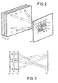
- the emission matrix 13 consists of a network of m ⁇ x modular light sources, collimated using a network 14 of microlenses or focusing fibers of the index gradient type for example.
- the beams thus generated are placed opposite a plate 15 of BSO material serving as a support for the recording of phase networks of suitable pitch and orientation. These networks are writable and erasable.
- the reading of the network is not destructive at the wavelengths considered, the incident beam is therefore deflected towards the desired address, and read on a matrix of photodetectors. This establishes the optical link between two subscribers.
- the essential interest of the device lies in the possibility of "crossing" in space all the light beams propagating independently between all the points of the input 13 and output 16 matrices.
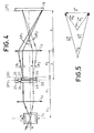
- the deflectors D i are, by way of nonlimiting example, constituted by galvanometric mirrors operating in random access in the two directions XY.
- Each deflection block Di can be numi of an optical device ensuring the conjugation of the deflectors X and Y.
- the deflector Di a mirror mounted "à la Cardan".
- the pivot point of this mirror is located at the focal point of the lens L i .
- a set of beams of directions parallel to the optical axis is thus obtained.
- deflector Dz we can consider by way of nonlimiting example two successive acousto-optical deflectors one acting along the vertical axis and the other along the horizontal axis in a plane perpendicular to the optical axis.
- This first deviation along the vertical axis is followed by a second deviation along the horizontal axis. It is obtained by the propagation in the medium 28 of acoustics generated by the transducer 27 itself attacked by a signal from the generator 26.
- the operation of this second deflector is similar to that of the first.
- the medium 15 is a medium which amplifies the deflection of the beams, the reading and writing being done at different wavelengths.
- the wave fronts of the beams that converge are plane, so the strata are parallel.
- the association of two devices of this type ensures the generation of a network of strata of pitch and orientation suitable for deflecting the reading beam towards the selected subscriber.
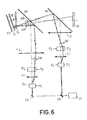
- These two devices can be arranged according to the diagram in FIG. 6 for the generation of the two interfering beams in the BSO crystal.
- This interference occurs in a three-dimensional medium.
- the physical characteristics of this medium and in particular the refractive index, are spatially modulated by a network of fringes due to the interference of these two incident beams. Due to this spatial modulation which a network of strata induces by gradient, any beam coming from the matrix of the photoemitting circuits will be diffracted in a chosen direction.
- the two writing beams come from the same source 21 which can be a HE-Cd laser, for example, after passing through a beam splitter 20.
- the addressing voltages Vi and V I , on the two deflectors D i and D ' i are equal: they make it possible to direct the writing beams at a given point of the BSO crystal 15.
- the addressing signals V 2 and V ' 2 on the deflectors D 2 and D' 2 are calculated so that the photoinduced grating is under Bragg incidence at the wavelength reading.
- the individual control of the angles ⁇ and ⁇ 'therefore makes it possible to generate any network by varying its pitch and the average orientation of the diffracting strata.
- Dichroic mirrors make it possible to reflect only the writing beams of known wavelength, and to transmit the other beams.
- FIGS. 7 and 8 the network of m ⁇ n light sources is collimated by a network of m ⁇ n microlenses. These beams are placed under oblique incidence ⁇ 0 so that the non-diffracted part of the incident wave is located outside the field of photoreceptor circuits which can be, for example, photodiodes.
- the diameter of the diffraction spot must be less than the pitch of the matrix of photoreceptor circuits.
- A is the wavelength of the beams coming from the matrix of the photoemitting circuits
- F is the distance between the plane of the network of strata and the plane of the photoreceptor circuits
- d is the width of the diffraction spot in the plane of the photoreceptor circuits and h the width of the strata useful for the diffraction of the incident beams in the photosensitive medium.
- F being equal to 600 millimeter, d to 0.9 micrometer, we obtain h equal to 540 micrometers.
- AR is the reading wavelength in the medium n, and AoR in the air.
- the time for writing and erasing the photoinduced network in the crystal is less than a millisecond.
- the diffraction efficiency of the photoinduced grating is 2 x 10 - 3 .
- the calculations carried out show that the inscriptions that the registration of all the networks is possible with galvanometric mirrors commercially available.
- the size of the mirrors is approximately 60 x 60 millimeters.
- the maximum deflection angle at the exit of the acousto-optic deflectors is 25 °.
- Such devices have a random access time of less than 10 milliseconds per point.
- the registration of photoinduced networks by creation of the space charge field in the BSO material is carried out at zero field by diffusion or by application of a transverse electric field generated by an interdigital comb for example.
- the proposed device ensures the spatial switching of 10 4 subscribers, in a time of less than 10 milliseconds whatever the subscriber considered in the matrix of light sources.
- the photoemitters can be optical fibers; optical fiber photoreceptors; and the photosensitive medium a monocrystalline slide of BSO. It is also possible to use the same number of photoemitting circuits and photoreceptor circuits.
Landscapes
- Engineering & Computer Science (AREA)
- Computer Networks & Wireless Communication (AREA)
- Holo Graphy (AREA)
- Use Of Switch Circuits For Exchanges And Methods Of Control Of Multiplex Exchanges (AREA)
Claims (11)
Applications Claiming Priority (2)
| Application Number | Priority Date | Filing Date | Title |
|---|---|---|---|
| FR8025910 | 1980-12-05 | ||
| FR8025910A FR2495873B1 (fr) | 1980-12-05 | 1980-12-05 | Dispositif de commutation de faisceaux optiques et central telephonique comprenant un tel dispositif |
Publications (2)
| Publication Number | Publication Date |
|---|---|
| EP0053957A1 EP0053957A1 (de) | 1982-06-16 |
| EP0053957B1 true EP0053957B1 (de) | 1985-07-10 |
Family
ID=9248746
Family Applications (1)
| Application Number | Title | Priority Date | Filing Date |
|---|---|---|---|
| EP81401785A Expired EP0053957B1 (de) | 1980-12-05 | 1981-11-10 | Vermittlungseinrichtung für optische Bündel und eine solche Einrichtung enthaltende Fernsprechvermittlungsanlage |
Country Status (6)
| Country | Link |
|---|---|
| US (1) | US4403352A (de) |
| EP (1) | EP0053957B1 (de) |
| JP (1) | JPS57120920A (de) |
| CA (1) | CA1173144A (de) |
| DE (1) | DE3171343D1 (de) |
| FR (1) | FR2495873B1 (de) |
Families Citing this family (15)
| Publication number | Priority date | Publication date | Assignee | Title |
|---|---|---|---|---|
| FR2518766A1 (fr) * | 1981-12-18 | 1983-06-24 | Thomson Csf | Dispositif de commutation de faisceaux optiques et central telephonique comprenant un tel dispositif |
| FR2544151B1 (fr) * | 1983-04-06 | 1985-06-21 | Thomson Csf | Dispositif de commutation spatiale de faisceaux optiques |
| US4705344A (en) * | 1984-12-19 | 1987-11-10 | American Telephone And Telegraph Company, At&T Bell Laboratories | Optical interconnection arrangement |
| US4703993A (en) * | 1984-12-19 | 1987-11-03 | American Telephone And Telegraph Company, At&T Bell Laboratories | Method and apparatus for making a device for optically interconnecting optical devices |
| US4764890A (en) * | 1984-12-19 | 1988-08-16 | American Telephone And Telegraph Company, At&T Bell Laboratories | Optical logic arrangement |
| GB2228386B (en) * | 1989-02-10 | 1993-09-29 | British Aerospace | Optical interconnection system |
| DE4011718A1 (de) * | 1990-04-11 | 1991-10-17 | Heidenhain Gmbh Dr Johannes | Integriert-optische sensoreinrichtung |
| US5090824A (en) * | 1990-07-31 | 1992-02-25 | Geo-Centers, Inc. | Fast optical switch having reduced light loss |
| FR2674391B1 (fr) * | 1991-03-19 | 1993-06-04 | Thomson Csf | Dispositif d'intercorrelation large bande et dispositif mettant en óoeuvre ce procede. |
| US5298964A (en) * | 1992-03-31 | 1994-03-29 | Geo-Center, Inc. | Optical stress sensing system with directional measurement capabilities |
| US5305136A (en) * | 1992-03-31 | 1994-04-19 | Geo-Centers, Inc. | Optically bidirectional fast optical switch having reduced light loss |
| FR2696014B1 (fr) * | 1992-09-18 | 1994-11-04 | Thomson Csf | Miroir à conjugaison de phase. |
| FR2755516B1 (fr) | 1996-11-05 | 1999-01-22 | Thomson Csf | Dispositif compact d'illumination |
| FR2819061B1 (fr) * | 2000-12-28 | 2003-04-11 | Thomson Csf | Dispositif de controle de polarisation dans une liaison optique |
| FR2860291B1 (fr) * | 2003-09-26 | 2005-11-18 | Thales Sa | Dispositif capteur de vitesse de rotation interferometrique a fibre optique |
Family Cites Families (5)
| Publication number | Priority date | Publication date | Assignee | Title |
|---|---|---|---|---|
| US3718383A (en) * | 1971-04-19 | 1973-02-27 | Eastman Kodak Co | Plastic optical element having refractive index gradient |
| DE2206098C3 (de) * | 1972-02-09 | 1980-03-13 | Philips Patentverwaltung Gmbh, 2000 Hamburg | Koppelfeld für ein Vermittlungssystem von Nachrichtenkanälen, vorzugsweise im optischen Frequenzbereich |
| FR2243573A1 (en) * | 1973-09-06 | 1975-04-04 | Treheux Michel | Broadband electro-optical coupler for telephony - uses point holography by scanning photo-matrix with laser's and LED's |
| US4074142A (en) * | 1975-09-10 | 1978-02-14 | Jackson Albert S | Optical cross-point switch |
| FR2385266A1 (fr) * | 1977-03-25 | 1978-10-20 | Thomson Csf | Dispositif de commutation electro-optique et autocommutateur telephonique comprenant un tel dispositif |
-
1980
- 1980-12-05 FR FR8025910A patent/FR2495873B1/fr not_active Expired
-
1981
- 1981-11-10 DE DE8181401785T patent/DE3171343D1/de not_active Expired
- 1981-11-10 EP EP81401785A patent/EP0053957B1/de not_active Expired
- 1981-12-01 CA CA000391267A patent/CA1173144A/en not_active Expired
- 1981-12-02 US US06/326,556 patent/US4403352A/en not_active Expired - Fee Related
- 1981-12-04 JP JP56194645A patent/JPS57120920A/ja active Pending
Non-Patent Citations (1)
| Title |
|---|
| Proc. Symp. Modern Optics, Microwave Res. Inst. Symp. Series, Vol. XVII, N.J., March 67 H. Kogelnik "Reconstructing response and efficiency of hologram gratings" pp. 605-617 * |
Also Published As
| Publication number | Publication date |
|---|---|
| EP0053957A1 (de) | 1982-06-16 |
| DE3171343D1 (en) | 1985-08-14 |
| FR2495873A1 (fr) | 1982-06-11 |
| FR2495873B1 (fr) | 1987-01-02 |
| JPS57120920A (en) | 1982-07-28 |
| CA1173144A (en) | 1984-08-21 |
| US4403352A (en) | 1983-09-06 |
Similar Documents
| Publication | Publication Date | Title |
|---|---|---|
| EP0083520B1 (de) | Lichtstrahlen-Schaltgerät insbesondere für Telefonzentrale | |
| EP0053957B1 (de) | Vermittlungseinrichtung für optische Bündel und eine solche Einrichtung enthaltende Fernsprechvermittlungsanlage | |
| US3831035A (en) | Switching network for information channels, preferably in the optical frequency range | |
| EP0067082B1 (de) | Kohärente Strahlungsquelle zur Erzeugung eines in der Fortpflanzungsrichtung regelbaren Strahlenbündels | |
| US5995251A (en) | Apparatus for holographic data storage | |
| EP0040114B1 (de) | Optische Echtzeitbeobachtungseinrichtung mit Abtastung | |
| US3604778A (en) | Fourier transform recording with random phase shifting | |
| US4256362A (en) | Phase-insensitive hologram readout technique | |
| EP0196933A1 (de) | Vorrichtung zur optischen Verbindung zwischen elektronischen Schaltkreisplatten in einem Kasten und Verfahren zu deren Herstellung | |
| JP2002508531A (ja) | スペックル平均化によるホログラフ記憶システムにおける散乱雑音の低減 | |
| EP0138668B1 (de) | Einrichtung zur Aufnahme eines kohärenten Bildes in einem multimoden-optischen Hohlraum | |
| WO1994010598A1 (fr) | Modulateur optique | |
| US5513022A (en) | Method and apparatus for direct transmission of an optical image | |
| EP0058592B1 (de) | Optische Anordnung zur Fouriertransformation und optischer Korrelator zu deren Anwendung | |
| EP0053052B1 (de) | Interferometrische Einrichtung zur Echtzeit-Sichtbarmachung der Verformungen von schwingenden Gegenständen | |
| FR2614136A1 (fr) | Dispositif de commande optique d'une antenne a balayage | |
| US3980389A (en) | Electro-optical deflection apparatus using holographic grating | |
| US3964032A (en) | Optical system for storing information | |
| EP0122192A1 (de) | Raumvielfach-Schalteinrichtung für optische Bündel | |
| FR2709827A1 (fr) | Dispositif optique d'imagerie permettant l'analyse spectrale d'une scène. | |
| US5963347A (en) | Holographic neurochip | |
| JP2000507004A (ja) | 増大した角度走査範囲を有する光学装置 | |
| EP0026128A1 (de) | Holografische Speichervorrichtung und optisches Informationsbehandlungssystem mit einer solchen Vorrichtung | |
| US4416512A (en) | Non-mechanical electromagnetic scanning device | |
| JP3036656B2 (ja) | 光スイッチ |
Legal Events
| Date | Code | Title | Description |
|---|---|---|---|
| PUAI | Public reference made under article 153(3) epc to a published international application that has entered the european phase |
Free format text: ORIGINAL CODE: 0009012 |
|
| AK | Designated contracting states |
Designated state(s): DE GB IT NL SE |
|
| 17P | Request for examination filed |
Effective date: 19820702 |
|
| ITF | It: translation for a ep patent filed | ||
| GRAA | (expected) grant |
Free format text: ORIGINAL CODE: 0009210 |
|
| AK | Designated contracting states |
Designated state(s): DE GB IT NL SE |
|
| REF | Corresponds to: |
Ref document number: 3171343 Country of ref document: DE Date of ref document: 19850814 |
|
| PLBE | No opposition filed within time limit |
Free format text: ORIGINAL CODE: 0009261 |
|
| STAA | Information on the status of an ep patent application or granted ep patent |
Free format text: STATUS: NO OPPOSITION FILED WITHIN TIME LIMIT |
|
| 26N | No opposition filed | ||
| PGFP | Annual fee paid to national office [announced via postgrant information from national office to epo] |
Ref country code: NL Payment date: 19871130 Year of fee payment: 7 |
|
| REG | Reference to a national code |
Ref country code: GB Ref legal event code: 746 |
|
| PGFP | Annual fee paid to national office [announced via postgrant information from national office to epo] |
Ref country code: DE Payment date: 19891023 Year of fee payment: 9 |
|
| PGFP | Annual fee paid to national office [announced via postgrant information from national office to epo] |
Ref country code: GB Payment date: 19891031 Year of fee payment: 9 |
|
| PG25 | Lapsed in a contracting state [announced via postgrant information from national office to epo] |
Ref country code: SE Effective date: 19891111 |
|
| PG25 | Lapsed in a contracting state [announced via postgrant information from national office to epo] |
Ref country code: NL Effective date: 19900601 |
|
| NLV4 | Nl: lapsed or anulled due to non-payment of the annual fee | ||
| PG25 | Lapsed in a contracting state [announced via postgrant information from national office to epo] |
Ref country code: GB Effective date: 19901110 |
|
| GBPC | Gb: european patent ceased through non-payment of renewal fee | ||
| PG25 | Lapsed in a contracting state [announced via postgrant information from national office to epo] |
Ref country code: DE Effective date: 19910801 |
|
| EUG | Se: european patent has lapsed |
Ref document number: 81401785.1 Effective date: 19900705 |