EP0054338A2 - Circuit logique à deux phases à technique MOS - Google Patents
Circuit logique à deux phases à technique MOS Download PDFInfo
- Publication number
- EP0054338A2 EP0054338A2 EP81201370A EP81201370A EP0054338A2 EP 0054338 A2 EP0054338 A2 EP 0054338A2 EP 81201370 A EP81201370 A EP 81201370A EP 81201370 A EP81201370 A EP 81201370A EP 0054338 A2 EP0054338 A2 EP 0054338A2
- Authority
- EP
- European Patent Office
- Prior art keywords
- transistors
- voltage
- logic circuit
- output
- transistor
- Prior art date
- Legal status (The legal status is an assumption and is not a legal conclusion. Google has not performed a legal analysis and makes no representation as to the accuracy of the status listed.)
- Granted
Links
Images
Classifications
-
- H—ELECTRICITY
- H03—ELECTRONIC CIRCUITRY
- H03K—PULSE TECHNIQUE
- H03K19/00—Logic circuits, i.e. having at least two inputs acting on one output; Inverting circuits
- H03K19/01—Modifications for accelerating switching
- H03K19/017—Modifications for accelerating switching in field-effect transistor circuits
- H03K19/01728—Modifications for accelerating switching in field-effect transistor circuits in synchronous circuits, i.e. by using clock signals
-
- H—ELECTRICITY
- H03—ELECTRONIC CIRCUITRY
- H03K—PULSE TECHNIQUE
- H03K19/00—Logic circuits, i.e. having at least two inputs acting on one output; Inverting circuits
- H03K19/0175—Coupling arrangements; Interface arrangements
- H03K19/0185—Coupling arrangements; Interface arrangements using field effect transistors only
- H03K19/018507—Interface arrangements
- H03K19/01855—Interface arrangements synchronous, i.e. using clock signals
-
- H—ELECTRICITY
- H03—ELECTRONIC CIRCUITRY
- H03K—PULSE TECHNIQUE
- H03K19/00—Logic circuits, i.e. having at least two inputs acting on one output; Inverting circuits
- H03K19/02—Logic circuits, i.e. having at least two inputs acting on one output; Inverting circuits using specified components
- H03K19/08—Logic circuits, i.e. having at least two inputs acting on one output; Inverting circuits using specified components using semiconductor devices
- H03K19/094—Logic circuits, i.e. having at least two inputs acting on one output; Inverting circuits using specified components using semiconductor devices using field-effect transistors
- H03K19/096—Synchronous circuits, i.e. using clock signals
Definitions
- the invention relates to a logic circuit in 2-phase MOS technology with several identical logic elements, each consisting of a series circuit of the MOS transistors receiving the input signals to be linked and a query MOS transistor receiving a query clock signal, one end of which each series connection with a reference potential and the other end of each series connection via a common charging MOS transistor, which receives the charging clock signal, the interrogation transistors and the charging transistor never being conductive at the same time, being connected to an operating voltage and that of the main electrode of the charging transistor facing away from the operating voltage and connected to the series circuits represents the output of the logic circuit to which the gate of at least one output MOS transistor is connected, which at a voltage at the output of the logic circuit between the operating voltage and a fraction / an e emits an indefinitely low signal.
- Such logic circuits are known, for example from DE-AS 17 87 011.
- a charging clock pulse 02 is alternately supplied and a query clock pulse ⁇ 1 thereafter in each case.
- the then conductive charging transistor charges the output of the logic circuit at least up to close to the operating voltage.
- the inputs of the transistors in the individual series connections receive the input signals to be linked.
- the charging transistor is blocked and the interrogation transistors that conduct each row are conductive Connect the circuit with the reference potential. If there is now a series circuit in which all the transistors are conductive without exception (fulfilled AND condition), the output of the logic circuit is discharged to the reference potential via this series circuit.
- each series connection represents a considerable capacitive load, so that the discharge over the completely conductive series connection takes a relatively long time. This reduces the switching speed of the entire logic circuit.
- the object of the invention is to provide a logic circuit of the type mentioned in the introduction, in which the highest possible switching speed and thus the highest possible repetition frequency of the clock signals is made possible even with the most unfavorable combination of the input signals to be linked.
- an additional MOS transistor is arranged in the connection of each series circuit to the charging MOS transistor and all additional transistors together receive such a signal at the gate that at least during the conductive phase of the interrogation transistors for voltages at the output of the logic circuit between the operating voltage and a value below the fraction thereof, any additional MOS Transistor between the charging MOS transistor and a series circuit with at least one blocked transistor is blocked.
- the additional transistors thus act similarly to diodes, which allow current to flow only when the charging transistor is conductive to charge the series circuit, but are blocked until a conductive series circuit has discharged the output to such an extent that the output transistor is blocked.
- a conductive series circuit only needs to discharge the capacitance at the output of the logic circuit, at least during this discharge time, but not the other charged series circuits.
- the additional transistors are expediently enhancement MOS transistors because they are the easiest to control for this purpose.
- the signal at the gates of the additional transistors can be a DC voltage with a value less than the sum of the lowest voltage at which the output MOS transistor connected to the output of the logic circuit still emits a clearly low signal, and the Threshold voltage of the additional transistors.
- the additional transistors of the non-conductive series circuits only become conductive when the voltage at the output of the logic circuit has dropped to such an extent that the output transistor emits the final, unambiguous output signal, so that the discharge which takes place more slowly as a result of the additional transistors which have become conductive no longer occurs affects the output signal of the output transistor.
- the signal at the gates of the additional transistors is the voltage at the output of the logic circuit.
- the additional transistors of the non-conductive series connections actually act like diodes over the entire voltage range, but the output of the connections k logic circuit loaded by the capacity of the gates of the additional transistors.
- the signal at the gates of the additional transistors is a clock signal whose voltage value in the case of conducting interrogation MOS transistors is less than the sum of the lowest voltage at which the output MOS transistor connected to the output of the logic circuit Transistor (T5) still emits a clearly low signal, and the threshold voltage of the additional transistors, and whose voltage value is greater, at least in the case of a conductive charging MOS transistor.
- the series circuits are charged to a higher voltage value during charging p Hase, so that in the subsequent interrogation phase, if none of the series circuits becomes conductive, the high level at the output of the logic circuit is more reliably guaranteed.
- the voltage value of the clock signal when the charging MOS transistor is conductive is equal to the operating voltage.
- Such a voltage value is easy to generate and causes a sufficiently high charging of all series circuits or at least of their upper points connected to the additional transistors.
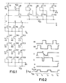
- the circuit shown in FIG. 1 contains only MOS transistors, which are therefore referred to only as transistors in the further description.
- MOS transistors which are therefore referred to only as transistors in the further description.
- three strands A, B and C are shown, each from egg ner series connection of several transistors exist. Only three strands are shown here as an example, while in practice a significantly larger number of strands with a likewise larger number of transistors is used in order to implement a correspondingly larger number of logic functions.
- the upper ends of the strands A, B and C are connected to one another and to a circuit point D which represents the output of the logic circuit and which is connected to the operating voltage V DD via a charging transistor T1 controlled by the clock signal 02.
- the gate of an output transistor T5 is connected to the output D via a transmission transistor T3 controlled by the clock signal ⁇ 1.
- the drain of the output transistor T5 is connected via a transistor T4 connected as a load resistor to the operating voltage V DD and via a further transmission transistor T6 controlled by the clock signal 02 to the gate of a second output transistor T8, the drain of which is again connected via a Load resistor switched transistor T7 is connected to the operating voltage V DD and to the output Q and to the gate of a third output transistor T10, the drain of which is connected to the operating voltage V DD and the further output QN via the transistor T9 operating as a load resistor.
- Transistors T4, T7 and T9 are depletion field effect transistors which are conductive and in this case act as current generators when their gates are connected to one of the main electrodes, as can be seen from the fact that the line indicating the main current path and opposite the gate is solid. while, inter alia, the transistors T5, T6, T8 and T10 are enhancement field-effect transistors, in which this line indicating the main current path is shown interrupted, since such transistors are only conductive when the potential at the gate is more positive than the threshold voltage V TH the bottom potential on one of the main electrodes. In both types of transistors, however, the main electrodes are interchangeable, ie a current can flow through the transistor in both directions, which is important for the later explanation.
- the transistor pairs T4 and T5, T7 and T8 as well as T9 and T10 each represent an inverter, which outputs the reference potential corresponding to the negative pole V SS of the operating voltage to which the enhancement transistor of each inverter is connected, if the Voltage at the gate of the enhancement transistor is higher than the switching voltage V T of the enhancement transistor, and which outputs the positive operating voltage V DD at the output at a lower voltage at the gate.
- This switching voltage is higher than the threshold voltage V TH of the enhancement transistor connected to the reference voltage V SS , because this must be controlled further into the conductive state until it can completely take over the current of the depletion transistor connected to the positive operating voltage.
- each inverter can be set within a certain range by appropriate geometric dimensioning of its two transistors.
- the last two inverters with transistors T6 to T10 represent a D flip-flop, which takes over the signal at node E with clock 02 and outputs it to the mutually complementary outputs Q and QN, and this signal also after the end of clock Q2 still maintains, as with blocked transfer transistor T6, the signal at the gate of the transistor T8 through the Gateka p aztician remains stored.
- This further processing of the output signal of the output transistor T5 by a D flip-flop represents only one possibility and is only mentioned here for example.
- Line A contains a series connection of several enhancement field-effect transistors.
- TAO which represents the interrogation transistor, has one main electrode connected to the reference potential V SS , and the gate of this transistor receives the clock signal 01.
- this interrogation transistor TAO can also be arranged at another point in the series circuit.
- the series connection of three further transistors TA1 to TA3 is connected to the other main electrode, the gates of which receive the signals to be linked via the input connections A1 to A3.
- the series connection ends with the transistor TA, which receives the signal V G at the gate and which is connected to the node D together with the corresponding transistors of the other strands.
- the transistors TB2 and TB3 are depletion field-effect transistors, which are always conductive, that is to say even when the signal at the inputs B2 and B3 is low.
- the series connection of line B is thus already completely conductive if, with correspondingly high signals at inputs VG and 01, only input B1 receives a high signal.
- the reason for this measure is that in practice there is a much larger number of individual strings, each with a much larger number of transistors, which are intended to decode different combinations of the same input signals, so that the entire arrangement as a matrix from the series connections of transistors and built these crossing input lines is.
- the input line which is to meet the AND condition in a special line even with a low signal, then leads to a depletion transistor. In the case of strand C, this is only the case, for example, with transistor TC2.
- Each line thus represents a NAND combination of another combination of input signals, which are OR-combined via the common connection with the circuit point.
- this circuit i.e. the time course of individual signals
- the charging clock signal ⁇ 2 becomes positive, which also makes node D positive, since the clock signal ⁇ 1 is simultaneously low and blocks all series connections via the transistors TAO, TBO, TCO etc.
- the circuit point D reaches a voltage which is lower by the threshold voltage V TH of the transistor T1 than the high value of the clock signal 02, which is assumed to be equal to the positive operating voltage V DD . This voltage is initially retained even after the end of the clock signal 02, since the circuit point D has a capacitance with respect to other circuit parts with a constant voltage, which maintains the charging for a certain time.
- the clock signal ⁇ 1 assumes a high value, so that the transistor T3 becomes conductive and transfers part of the charge of the node D to the capacitance of the gate of the transistor T5.
- the transistor T2 connected as a capacitor is provided seen that transfers a corresponding or slightly larger charge from the clock signal 01 to the node D. Since the gate of transistor T5 thus becomes positive, node E assumes voltage V SS . At this time, however, the transistor T6 is blocked because the clock signal 02 is low.
- the transistors TAO, TBO and TCO also become conductive.
- the transistors TA, TB and TC are initially disregarded or replaced by a permanently conductive connection.
- the signals had been applied to the inputs A1 to A3, B1 to B3 and C1 to C3, and signals are accepted which bring the transistors TA1 to TA3 and TC3 into conduction and the transistors TB1 and Lock TC1.
- the transistors TB2, TB3 and TC2 are conductive anyway, since they are depletion transistors.
- the series connection of strand A up to and including the connection of transistors TAO and TA1 is thus charged to the potential of node D, correspondingly the series connection of strand B up to the connection between transistors TB1 and TB2 and the series connection of strand C up to the connection of the transistors TC1 and TC2.
- the transistors TAO to TCO become conductive, only the series connection of the strand A forms a conductive connection between the circuit point D and the reference potential V SS , so that the circuit point D is discharged above it.
- the transistors TA to TC are intended to be replaced by a conductive connection, the strings B and C must also be discharged up to the blocked transistors TB1 and TC1.
- the signal V G is a DC voltage with the value 2.5V.
- the transistors TB and TC remain at the limit of the conductive state, so that no current can flow from the capacitances which represent the transistors of the strands B and C to the switching point D and thus via the strand A to V SS .
- inverter T4 / T5 is dimensioned such that it is at an input voltage of 1, 5 V already generated high potential at node E, the delay in the discharge, which begins at the voltage of 1.5 V at node D, no longer affects the final signal at node E, so that the clock signal 01 already before complete discharge of the circuit point D can return to OV, since then a voltage remains at the gate of the transistor T5, which still has a high potential at the point E.
- curve D in which the switching voltage of inverter T4 / T5 is shown as a horizontal line through the discharge curve, curve E being high again after this intersection.
- the inputs A1 to A3 etc. of the strands A, B and C are supplied with other signals, which may now have a combination such that none of the strands with that at the time t 3 beginning following clock signal ⁇ 1 is conductive and the node D is not discharged.
- the switching point E thus goes to the reference potential V SS at the time t 3 , and with the next clock signal 02 at the time t 4 this potential is transferred to the flip-flop via the transfer transistor T6, so that the output Q now assumes a high potential.
- a second possibility for the voltage V G at the gates of the transistors TA, TB and TC is to connect them to the circuit point D, as is indicated by dashed lines in FIG. 1.
- the strands are charged during the clock signal 02 to a voltage which is below the voltage of the node D by the threshold voltage of the transistors TA, TB and TC. If this circuit point D is then discharged by a conductive strand, for example strand A, only the transistor TA becomes conductive, while the transistors TB and TC up to a maximum discharge at which the Always block voltage of node D by the threshold voltage of transistor TA above voltage V SS .
- the transistors TB and TC of blocked strands thus behave like diodes which only allow charging or recharging of the flow from the switching point D via the transistor T1, but no discharge of blocked strings via the switching point D.
- a uniform distribution of the charge then occurs in strand B, that is to say all the capacitances in the strand between the source of the additional transistor TB and the drain of the transistor TB1 adjust approximately to the same voltage. To do this, however, charge must flow from the drain terminal of transistor TB3, ie its voltage drops below V G - VTH, so that transistor TB3 can become conductive and then draw off charges from node D.
- the charges stored on the end of the strand facing the circuit point D can be distributed uniformly over the entire strand up to the first blocked transistor.
- the clocking of V G thus increases reliability or allows higher clock frequencies.
- the transistors TA, TB and TC receive such a signal V G at the gate that these transistors are blocked in the case of non-conductive strands until the output signal has reached its final value.
Landscapes
- Engineering & Computer Science (AREA)
- Computer Hardware Design (AREA)
- Physics & Mathematics (AREA)
- Computing Systems (AREA)
- General Engineering & Computer Science (AREA)
- Mathematical Physics (AREA)
- Power Engineering (AREA)
- Logic Circuits (AREA)
- Compression, Expansion, Code Conversion, And Decoders (AREA)
Applications Claiming Priority (2)
| Application Number | Priority Date | Filing Date | Title |
|---|---|---|---|
| DE3047222 | 1980-12-15 | ||
| DE19803047222 DE3047222A1 (de) | 1980-12-15 | 1980-12-15 | Verknuepfungsschaltung in 2-phasen-mos-technik |
Publications (3)
| Publication Number | Publication Date |
|---|---|
| EP0054338A2 true EP0054338A2 (fr) | 1982-06-23 |
| EP0054338A3 EP0054338A3 (en) | 1983-01-05 |
| EP0054338B1 EP0054338B1 (fr) | 1984-05-30 |
Family
ID=6119216
Family Applications (1)
| Application Number | Title | Priority Date | Filing Date |
|---|---|---|---|
| EP81201370A Expired EP0054338B1 (fr) | 1980-12-15 | 1981-12-14 | Circuit logique à deux phases à technique MOS |
Country Status (5)
| Country | Link |
|---|---|
| US (1) | US4468575A (fr) |
| EP (1) | EP0054338B1 (fr) |
| JP (1) | JPS57124941A (fr) |
| CA (1) | CA1180063A (fr) |
| DE (2) | DE3047222A1 (fr) |
Families Citing this family (6)
| Publication number | Priority date | Publication date | Assignee | Title |
|---|---|---|---|---|
| US4851714A (en) * | 1987-12-11 | 1989-07-25 | American Telephone And Telgraph Company, At&T Bell Laboratories | Multiple output field effect transistor logic |
| US5389835A (en) * | 1991-04-12 | 1995-02-14 | Hewlett-Packard Company | Vector logic method and dynamic mousetrap logic gate for a self-timed monotonic logic progression |
| US5208490A (en) * | 1991-04-12 | 1993-05-04 | Hewlett-Packard Company | Functionally complete family of self-timed dynamic logic circuits |
| RU2132591C1 (ru) * | 1998-04-24 | 1999-06-27 | Институт проблем управления РАН | Каскадное логическое устройство на кмдп транзисторах |
| RU2209507C1 (ru) * | 2002-05-13 | 2003-07-27 | Институт проблем управления им. В.А. Трапезникова РАН | Парафазное каскадное логическое устройство на кмдп транзисторах |
| RU2209508C1 (ru) * | 2002-05-13 | 2003-07-27 | Институт проблем управления им. В.А.Трапезникова РАН | Парафазный логический элемент каскадных устройств на кмдп транзисторах |
Family Cites Families (9)
| Publication number | Priority date | Publication date | Assignee | Title |
|---|---|---|---|---|
| US3526783A (en) * | 1966-01-28 | 1970-09-01 | North American Rockwell | Multiphase gate usable in multiple phase gating systems |
| US3573487A (en) * | 1969-03-05 | 1971-04-06 | North American Rockwell | High speed multiphase gate |
| US3601627A (en) * | 1970-07-13 | 1971-08-24 | North American Rockwell | Multiple phase logic gates for shift register stages |
| US4040015A (en) * | 1974-04-16 | 1977-08-02 | Hitachi, Ltd. | Complementary mos logic circuit |
| US3982138A (en) * | 1974-10-09 | 1976-09-21 | Rockwell International Corporation | High speed-low cost, clock controlled CMOS logic implementation |
| US4048518A (en) * | 1976-02-10 | 1977-09-13 | Intel Corporation | MOS buffer circuit |
| US4107548A (en) * | 1976-03-05 | 1978-08-15 | Hitachi, Ltd. | Ratioless type MIS logic circuit |
| GB1575741A (en) * | 1977-01-17 | 1980-09-24 | Philips Electronic Associated | Integrated circuits |
| DE3001389A1 (de) * | 1980-01-16 | 1981-07-23 | Philips Patentverwaltung Gmbh, 2000 Hamburg | Schaltungsanordnung in integrierter schaltungstechnik mit feldeffekttransistoren |
-
1980
- 1980-12-15 DE DE19803047222 patent/DE3047222A1/de not_active Withdrawn
-
1981
- 1981-12-09 US US06/328,876 patent/US4468575A/en not_active Expired - Fee Related
- 1981-12-10 CA CA000391974A patent/CA1180063A/fr not_active Expired
- 1981-12-14 DE DE8181201370T patent/DE3163929D1/de not_active Expired
- 1981-12-14 JP JP56200256A patent/JPS57124941A/ja active Granted
- 1981-12-14 EP EP81201370A patent/EP0054338B1/fr not_active Expired
Also Published As
| Publication number | Publication date |
|---|---|
| JPS57124941A (en) | 1982-08-04 |
| DE3047222A1 (de) | 1982-07-15 |
| JPH0220019B2 (fr) | 1990-05-07 |
| EP0054338A3 (en) | 1983-01-05 |
| DE3163929D1 (en) | 1984-07-05 |
| CA1180063A (fr) | 1984-12-27 |
| US4468575A (en) | 1984-08-28 |
| EP0054338B1 (fr) | 1984-05-30 |
Similar Documents
| Publication | Publication Date | Title |
|---|---|---|
| DE2553517C3 (de) | Verzögerungsschaltung mit Feldeffekttransistoren | |
| DE2541131C2 (de) | Schaltungsanordnung zum Konstanthalten der Schaltverzögerung von FET-Inverterstufen in einer integrierten Schaltung | |
| DE2545450A1 (de) | Bootstrapschaltung mit feldeffekttransistoren | |
| DE2359151A1 (de) | Steuerschaltung fuer feldeffekttransistoren | |
| DE3904901A1 (de) | Integrierte gegentakt-ausgangsstufe | |
| DE3050199C2 (de) | Logikschaltung | |
| DE2356974A1 (de) | Aus feldeffekttransistoren aufgebaute gegentakt-treiberschaltung fuer digitale anwendungen | |
| DE2816980C3 (de) | FET-Treiberschaltung mit kurzen Schaltzeiten | |
| DE1474388C3 (de) | Schieberegisterspeicherstufe mit Feldeffekttransistoren | |
| DE69232170T2 (de) | Puffer mit niedrigem Rauschen | |
| DE2346568C3 (de) | Hybrider Zweitakt-Verriegelungsschaltkreis mit Zwischenspeicherung | |
| EP0020379B1 (fr) | Commutateur inverseur de tension | |
| DE2835692C3 (de) | Binäres logisches ODER-Glied für programmierte logische Anordnungen | |
| DE102021116029A1 (de) | Hochgeschwindigkeits-gatetreiberschaltung | |
| DE2415098A1 (de) | Ausschnittdetektor | |
| EP0054338B1 (fr) | Circuit logique à deux phases à technique MOS | |
| DE3343700C2 (fr) | ||
| DE2754987A1 (de) | Leistungslose halbleiter-speichervorrichtung | |
| DE2851111C2 (de) | Zweidimensionale Analog-Speicheranordnung | |
| DE2255210C3 (de) | Datenspeicherschaltung | |
| DE69113414T2 (de) | Integrierte Konstantstromversorgung. | |
| DE2435454A1 (de) | Dynamischer binaerzaehler | |
| DE3108342A1 (de) | Dynamische schieberegisterschaltung | |
| DE2450882A1 (de) | Komplementaere mos-logische schaltung | |
| DE2651422C2 (de) | Ladungsspeicher mit Halbleiterelementen |
Legal Events
| Date | Code | Title | Description |
|---|---|---|---|
| PUAI | Public reference made under article 153(3) epc to a published international application that has entered the european phase |
Free format text: ORIGINAL CODE: 0009012 |
|
| 17P | Request for examination filed |
Effective date: 19811214 |
|
| AK | Designated contracting states |
Designated state(s): DE FR GB |
|
| RAP1 | Party data changed (applicant data changed or rights of an application transferred) |
Owner name: N.V. PHILIPS' GLOEILAMPENFABRIEKEN Owner name: PHILIPS PATENTVERWALTUNG GMBH |
|
| PUAL | Search report despatched |
Free format text: ORIGINAL CODE: 0009013 |
|
| AK | Designated contracting states |
Designated state(s): DE FR GB |
|
| GRAA | (expected) grant |
Free format text: ORIGINAL CODE: 0009210 |
|
| AK | Designated contracting states |
Designated state(s): DE FR GB |
|
| REF | Corresponds to: |
Ref document number: 3163929 Country of ref document: DE Date of ref document: 19840705 |
|
| ET | Fr: translation filed | ||
| PLBE | No opposition filed within time limit |
Free format text: ORIGINAL CODE: 0009261 |
|
| STAA | Information on the status of an ep patent application or granted ep patent |
Free format text: STATUS: NO OPPOSITION FILED WITHIN TIME LIMIT |
|
| 26N | No opposition filed | ||
| PGFP | Annual fee paid to national office [announced via postgrant information from national office to epo] |
Ref country code: FR Payment date: 19891219 Year of fee payment: 9 |
|
| PGFP | Annual fee paid to national office [announced via postgrant information from national office to epo] |
Ref country code: GB Payment date: 19891231 Year of fee payment: 9 |
|
| PGFP | Annual fee paid to national office [announced via postgrant information from national office to epo] |
Ref country code: DE Payment date: 19900221 Year of fee payment: 9 |
|
| PG25 | Lapsed in a contracting state [announced via postgrant information from national office to epo] |
Ref country code: GB Effective date: 19901214 |
|
| GBPC | Gb: european patent ceased through non-payment of renewal fee | ||
| PG25 | Lapsed in a contracting state [announced via postgrant information from national office to epo] |
Ref country code: FR Effective date: 19910830 |
|
| PG25 | Lapsed in a contracting state [announced via postgrant information from national office to epo] |
Ref country code: DE Effective date: 19910903 |
|
| REG | Reference to a national code |
Ref country code: FR Ref legal event code: ST |