EP0054596B1 - Verfahren für die Inspektion und die automatische Sortierung von Objekten, die Konfigurationen mit dimensionellen Toleranzen aufweisen und platzabhängige Kriterien für die Verwerfung, Anlage und Schaltung dafür - Google Patents
Verfahren für die Inspektion und die automatische Sortierung von Objekten, die Konfigurationen mit dimensionellen Toleranzen aufweisen und platzabhängige Kriterien für die Verwerfung, Anlage und Schaltung dafür Download PDFInfo
- Publication number
- EP0054596B1 EP0054596B1 EP80430030A EP80430030A EP0054596B1 EP 0054596 B1 EP0054596 B1 EP 0054596B1 EP 80430030 A EP80430030 A EP 80430030A EP 80430030 A EP80430030 A EP 80430030A EP 0054596 B1 EP0054596 B1 EP 0054596B1
- Authority
- EP
- European Patent Office
- Prior art keywords
- ref
- set forth
- image
- images
- exa
- Prior art date
- Legal status (The legal status is an assumption and is not a legal conclusion. Google has not performed a legal analysis and makes no representation as to the accuracy of the status listed.)
- Expired
Links
Images







Classifications
-
- G—PHYSICS
- G03—PHOTOGRAPHY; CINEMATOGRAPHY; ANALOGOUS TECHNIQUES USING WAVES OTHER THAN OPTICAL WAVES; ELECTROGRAPHY; HOLOGRAPHY
- G03F—PHOTOMECHANICAL PRODUCTION OF TEXTURED OR PATTERNED SURFACES, e.g. FOR PRINTING, FOR PROCESSING OF SEMICONDUCTOR DEVICES; MATERIALS THEREFOR; ORIGINALS THEREFOR; APPARATUS SPECIALLY ADAPTED THEREFOR
- G03F7/00—Photomechanical, e.g. photolithographic, production of textured or patterned surfaces, e.g. printing surfaces; Materials therefor, e.g. comprising photoresists; Apparatus specially adapted therefor
- G03F7/70—Microphotolithographic exposure; Apparatus therefor
- G03F7/70483—Information management; Active and passive control; Testing; Wafer monitoring, e.g. pattern monitoring
- G03F7/70605—Workpiece metrology
- G03F7/70616—Monitoring the printed patterns
-
- B—PERFORMING OPERATIONS; TRANSPORTING
- B07—SEPARATING SOLIDS FROM SOLIDS; SORTING
- B07C—POSTAL SORTING; SORTING INDIVIDUAL ARTICLES, OR BULK MATERIAL FIT TO BE SORTED PIECE-MEAL, e.g. BY PICKING
- B07C5/00—Sorting according to a characteristic or feature of the articles or material being sorted, e.g. by control effected by devices which detect or measure such characteristic or feature; Sorting by manually actuated devices, e.g. switches
- B07C5/04—Sorting according to size
- B07C5/10—Sorting according to size measured by light-responsive means
-
- G—PHYSICS
- G01—MEASURING; TESTING
- G01R—MEASURING ELECTRIC VARIABLES; MEASURING MAGNETIC VARIABLES
- G01R31/00—Arrangements for testing electric properties; Arrangements for locating electric faults; Arrangements for electrical testing characterised by what is being tested not provided for elsewhere
- G01R31/28—Testing of electronic circuits, e.g. by signal tracer
- G01R31/302—Contactless testing
- G01R31/308—Contactless testing using non-ionising electromagnetic radiation, e.g. optical radiation
-
- G—PHYSICS
- G06—COMPUTING OR CALCULATING; COUNTING
- G06T—IMAGE DATA PROCESSING OR GENERATION, IN GENERAL
- G06T7/00—Image analysis
- G06T7/0002—Inspection of images, e.g. flaw detection
- G06T7/0004—Industrial image inspection
- G06T7/001—Industrial image inspection using an image reference approach
-
- G—PHYSICS
- G06—COMPUTING OR CALCULATING; COUNTING
- G06T—IMAGE DATA PROCESSING OR GENERATION, IN GENERAL
- G06T2207/00—Indexing scheme for image analysis or image enhancement
- G06T2207/30—Subject of image; Context of image processing
- G06T2207/30108—Industrial image inspection
- G06T2207/30141—Printed circuit board [PCB]
-
- G—PHYSICS
- G06—COMPUTING OR CALCULATING; COUNTING
- G06T—IMAGE DATA PROCESSING OR GENERATION, IN GENERAL
- G06T2207/00—Indexing scheme for image analysis or image enhancement
- G06T2207/30—Subject of image; Context of image processing
- G06T2207/30108—Industrial image inspection
- G06T2207/30148—Semiconductor; IC; Wafer
Definitions
- the present invention relates on the one hand to a method of contactless inspection and automatic sorting of objects having dimensional tolerances and rejection criteria varying according to the inspected location of the object, and on the other hand its equipment and the implementation circuits. It relates more particularly to a method of contactless inspection and automatic sorting of objects having configurations having dimensional tolerances and rejection criteria varying according to the place inspected, such as printed circuits, masks, modules and Integrated circuit chips, used in the semiconductor industry, which use basic transformations of mathematical morphology and set theory. It also relates to its equipment and the processing circuits produced around a digital computer.
- French patent FR-A 2 095 523 shows an apparatus for detecting faults by optical scanning.
- This device mainly finds application in the field of manufacturing photo masks.
- This device which is applicable to the control of objects having configurations with variable tolerances depending on the location, can only work if the object to be examined has repetitive configurations; moreover, the reference object is a special object, which does not belong to the family of objects to be examined, and which is therefore specially constructed to take account of certain specificities of the object to be examined.
- a first object of the invention is to propose a method and an equipment which make it possible to automate the inspection and the sorting of objects having configurations with dimensional tolerances and variable rejection criteria and, which avoid resorting to sorting. manual optics.
- Another object of the present invention is to provide a method and equipment for inspecting and sorting objects having configurations with tolerances and rejection criteria that vary according to the location of said configurations.
- Another object of the invention is to propose a method and equipment for detecting faults, of an object to be examined, from a reference object of the same family.
- Another object of the invention is to propose a method and equipment which allow the inspection and sorting of objects having configurations with tolerances and rejection criteria varying according to the location making it possible to determine whether the object to be examine is operational within prescribed limits, based on previously determined rejection criteria.
- Another object of the invention is to propose a method and an equipment which allow the inspection and sorting of objects having configurations with tolerances and rejection criteria varying according to the location according to which said rejection criteria will be developed. automatically from a reference object during a preliminary step of the process.
- Yet another object of the invention is to provide a method and equipment for inspecting and sorting objects having configurations with tolerances and rejection criteria varying according to the location according to which the necessary capacity of the memory for perform the functions of adjustment to variable tolerances and of analysis according to variable rejection criteria, is very small compared to the number of bits representative of the image (for example 20 memory lines of 2048 bits for an image which can include 2048 ( or more) 2048-bit lines).
- the subject of the present invention is therefore, on the one hand, an automatic object inspection and sorting method as defined in claim 1 and, on the other hand, an apparatus for automatic object inspection and sorting. , which apparatus has the characteristics indicated in claim 17.
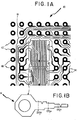
- FIG. 1A An electronic module 10, a portion of which is shown in FIG. 1A is a good example of this category of objects.
- the metal conductors 11 formed on the ceramic substrate have different widths and directions. Practically the conductors can have three widths: 250, 125 and 100 p and follow four directions: 0, 45, 90 and 135 °.
- the metallization tabs 12 which surround the pins 13 have an octagonal or derived shape.
- the conductors generally connect a tab 12 to a contact pad 14 which receives a solder ball from the chip (not shown).
- the control instructions specify the minimum dimensions of the conductors, by a certain percentage of their nominal width. This percentage is generally the same for all drivers. The maximum dimensions, for their part, depend on the interconductive space to be observed on the substrate.
- the same defect may or may not be acceptable depending on its location, for example the same lack of defect is unimportant in the conductor of width 250 ⁇ , while it is catastrophic for the conductor of width 100 ⁇ (see Figure 1 B) and that it then leads to the rejection of the module. It will then be understood that the rejection criterion will also have to take account of the region analyzed. Each time a fault is detected, it will have to be associated with the rejection criteria (s) established for this region.
- the images of the reference module (t ref ) and the sample module (l exa ). are captured, sampled and quantified, then thresholded, cleaned and framed to provide binary or electronic images, respectively I REF and I EXA .
- the image of the reference module is adjusted to the maximum and minimum dimensional tolerances in two different ways. We obtain (I REF ) max and (I REF ) min . These images are compared with the image of the sample module I ExA to give an image of the defects of the "lack" type and an image of the defects of the "extension” type.
- the fault images are scanned by an analysis window to determine whether they are acceptable or not.
- An embodiment of the present invention is characterized by the presence of a synchronization and addressing circuit associated with a memory, which for each point M of X, Y coordinates analyzed performs a double function. It first determines the value of the dimensional tolerance for this point and acts on the block of adjustment to the dimensional tolerances. In other words, the modulation of I REF to dimensional tolerances, performed before the comparison operation, is variable depending on the location.
- this circuit acts after the comparison operation on the image of the defects taking account of the delays, it determines the rejection criteria (practically a maximum acceptable size of the defect) for this point and supplies them to a block d 'defect analysis consisting mainly of calculation and comparison circuits.
- Boolean operations such as union, intersection and inversion will be used to process the electronic images and highlight the defects.
- other operations will be necessary to clean up the images or modify them taking into account the minimum and maximum dimensional tolerances of the circuits, these operations which fall under the mathematical morphology-essentially erosion and dilation-are the subject below. after a brief reminder.
- a and B be two sets of R2.
- AO + B a new set denoted AO + B such that: in other words, a point x of space R2 belongs to the dilate of A by B if and only if the translate of B par'OX meets A.
- the set B is called the structuring element.
- a and B be two sets of R2.
- a point y in space R2 belongs to the disc if the distance separating this point from the center is less than or equal to the radius.
- the distance between a point x and a set X of R2 is defined by the disc with center 0 and radius p, that is D (0, p) is denoted pD.
- the opening it is erosion followed by a dilation either (A ⁇ B) ⁇ B and
- the closure it is the expansion followed by an erosion either (A ⁇ B) ⁇ B
- erosion removes isolated parts smaller than the structuring element from the image (it is the same for expansion on A °).
- the opening removes from A all the parts smaller than the structuring element without changing the rest of the image (the closing has an identical effect on A C ).
- the images of the reference module (I ref ) and of the module to be examined ( exa ) provided by the sensor are, for example, in black and white with all the gray levels. These analog images are first sampled, according to a hexagonal or square frame, for example. The amplitude of the signal is quantified at each point of the image, and this information is coded on 4 bits.
- the images can have a number of lines and bits per line which varies according to the applications. In general 1024 or 2048 lines are satisfactory numbers for the majority of applications. In the present application, 2048 lines of 2048 bits each are chosen, that is to say with a 2.54 ⁇ 2.54 cm module, a pitch of 12.5 ⁇ between two image points (pixels). This results in approximately 4 million points to be treated.
- the choice of the threshold can be done in different ways, in particular by processing the images by region. We detect the threshold of each region from its histogram. The resulting threshold image is then the composition of all the threshold regions.
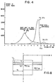
- An example of a histogram characteristic of an image of this type is given by the other curve of FIG. 4. In this case experience shows that the value of the threshold N TH can be chosen equal to 7.
- an automatic threshold detection can be done automatically by program by analyzing the histogram of the intensities of the image points of the analyzed image.
- the cleaning is carried out by an erosion which removes all the image points relating to the noise.
- the size of the structuring element that will erode the image must be less than the size of the smallest defect that must be detected.
- the isolated parts smaller than the size of erosion disappear while the others remain and are will be subsequently reconstituted by a dilation of the same size (overall the operation constitutes an opening).
- the dilation operation is carried out symmetrically: we erode the complementary image of the frame and we take the complement of the result, according to the relationship explained below:
- Cleaning can also be carried out after the framing step. Finally, this step can be optional depending on the quality of the images.
- FIG. 5 An example of an erosion operation is clearly shown in FIG. 5, a portion of conductor has been chosen as the initial image.
- a structuring element in the form of a cross or circle may be used (approximately).
- the size and pattern of the structuring element may vary depending on the type of application. In the present description, the square grid and a structuring element in the shape of a circle and of variable size will be used alone for the purpose of the simplicity of the presentation.
- the number of image points (pixels) can vary from 500,000 to 10 million and more depending on the application.
- FIG. 6 there are shown diagrammatically two patterns, one belonging to the image of the reference module I ref and the other to the image of the sample module, I exa , this latter pattern is misaligned with respect to that of the reference image.
- These patterns can be portions of markers or markers which are commonly used for aligning masks, modules, etc.
- a program is used to calculate the offset between the two images, at x and at y.
- the program only processes a limited group p of rows for the offset in x, and q columns for the offset in y.
- This program therefore consists in analyzing the function I (M x ) which represents the hatched area, according to the different values of M x (offset in x between the two images).
- I (My) is shown in Figure 8. This figure shows that a first attempt (1 1 ) to the right is in the wrong direction since I 1 > I, then to the left, the minimum is therefore obtained for an increment towards the negative y.
- This cropping step can be easily performed using a computer program.
- the pattern of I ref must overlap the corresponding pattern of I exa . This can be ensured by rough framing performed when capturing images. After having successively entered, sampled, quantified, thresholded, cleaned and framed, the binary images obtained are noted I REF , for the resulting image of the reference module and I EXA for the resulting image of the module to be examined.
- the cropping can be done either in the plane (x, y, ⁇ ) or even in space (x, y, z).
- the objects to be compared are essentially masks (reticles), microchips of integrated circuits, and electronic modules. In all cases there are dimensional tolerances for the patterns of these objects, for example with regard to the modules, the width of the conductive lines.
- FIGS. 9 and 10 defects can take various forms, some of the most characteristic of which are shown in FIGS. 9 and 10.
- step 5 of FIG. 3 With modules having variable tolerances according to the locations, the processing principle which has just been described remains the same (step 5 of FIG. 3), the process must be arranged so that the adjustment to the dimensional tolerances and the criteria of rejection are a function of the region.
- the structuring element of operation 5 ' ensuring adjustment to variable tolerances and the rejection criteria of operation 5 "' are essentially variable depending on the location.
- Figure 3 appears a device which bears the reference 7 and which is essential for the implementation of the present invention. This synchronization and addressing device ensures that the order and the content of the operations (in real time) are appropriate.
- I exa (and possibly I ref ) it controls for each pixel the operations of adjustment to dimensional tolerances (5 ') and analysis of the defect with regard to the rejection criteria for this pixel (5 "').
- the device 7 is associated with a memory which contains two data tables, one for faults of the "lack" type, one for faults of the "extension” type.
- the first table contains for each pixel the data: value of the dimensional tolerance and the rejection criteria for this point.
- the analysis of faults of the missing type in fact only requires knowledge of the width and direction of the conductor containing the analyzed pixel, it is therefore from these two pieces of information that the aforementioned data are developed.
- the two data will make it possible to adjust I REF to the dimensional tolerances and to provide the rejection criteria for each pixel.
- the information relating to the width and the direction of the conductors is therefore determined beforehand, it is used as a basis for the calculation of the useful data: tolerance value and rejection criteria, which will be stored in a memory in the form of
- extension type faults requires the storage in a memory of a second table which contains the useful data: tolerance value and rejection criteria for each pixel of the image, calculated from the information : width and direction of the inter-conductor space.
- the first table will be made up from I REF while the second table will be made up from I REF c .
- the conductors could have three widths: 100, 125 and 250 p and four directions: 0, 45, 90 and 135 °.
- For each pixel of a determined conductor of I REF it is necessary to determine the width and the direction of the conductor which contains it. For this, the number of pixels is calculated according to each of the four directions belonging to this conductor.
- a computer program must allow the driver's width and orientation to be determined without manual intervention. This process requires approximately 16 bits per pixel, or 4.2 million 16-bit words for IREF.
- I REF This quantity is obviously too large with respect to the memory space available practically in the memory.
- I REF regions are preferably the squares of a checkerboard which virtually overlap with I REF .
- At each square of the checkerboard will be associated dimensional tolerance and rejection criteria, respectively for defects of the "lack" and "extension” types.
- We choose for each square a size of 16x16 pixels, which gives only 16984 words of 16 bits to store. This size of square was chosen so as to optimize the necessary memory space and so that the density of conductors inside the square is minimum: two conductors per square at most.
- the invention is not limited to this choice.
- the size of the square allows two (or more) conductors per square, we can base our on the following rules: if the two conductors are identical, the widths and directions calculated for all the pixels of the square are identical. The rejection criterion and the width of the dimensional tolerance can easily be deduced from these values. In the case where the two conductors have different widths and / or directions, the smallest value of the tolerances calculated for all the pixels of the square and the most strict rejection criterion will be retained.
- control instructions For each conductor width, the control instructions define the acceptable size of the defects. Parameters other than the width can also be taken into account, for example: the length of the defect for a determined width of the conductor. For example, the following instructions can be found for a conductor whose nominal width L is equal to 125 ⁇ t.
- the parameters X, k, and A which obviously vary with the widths of the conductors, therefore constitute the basis of the rejection criteria for each square.
- these instructions will be applied by comparison not with I REF but with (I REF ) min (that is to say after adjustment of the reference image to the dimensional tolerances N).
- the projections of the lack of defect will be calculated in the direction of the conductor (width 1 of the defect) and in the perpendicular direction (length d of the defect). This determination is important, the rejection criteria being essentially based on the comparison of d and 1 with k L min and X% L min , L min ⁇ A respectively, for a determined orientation ( ⁇ ).
- FIG. 11B an interconnecting space 11b and two acceptable faults 18 and 19 have been shown, the projections h 1 and h 2 of which verify the rule ⁇ L ′ min -B.
- the size of the expansion (N ′) and the rejection criteria are those of the narrowest interconnecting space.
- N ′ the projections of the fault must be calculated in the four directions, and in each of the directions the rule must be checked.
- the size of the expansion and the rejection criteria will be those of the narrowest space.
- the parameters ⁇ , X, A, k and L are combined together using a calculator to represent the rejection criteria, which as we saw above are essentially functions of 6, L min -A, X% L min and k L min .
- the dimensional tolerance useful for eroding I REF is NI and the rejection criteria are ⁇ i, L min -A i , X,% L i , min ' ki L i min which give the orientation and size of acceptable defects.
- a similar fault table No. 2 ("extension" type) is also established.
- N ' the dimensional tolerance
- ⁇ i and B i the parameters ⁇ i and B i .
- each pixel of I EXA will be associated with the data corresponding to the square that contains it.
- the present method requires the simultaneous addressing of the X and Y coordinates of the point analyzed and of the square which contains it so that the corresponding words stored in memory can be available and act after decoding within the framework of the various operations of step 5.
- a example will be explained with an image of 16x16 pixels (256 image points) and with a checkerboard of sixteen squares; the dimension of each square being 4x4 pixels.
- Addressing X is done on 4 bits A, B, C, D, addressing Y is also done on 4 bits E, F, G, H.
- AB most significant bits of X
- EFAB most significant bits of Y
- the intermediate table includes the crossing lengths of all the pixels of value 1 in the image.
- the fourth parameter is assigned to the fourth word in the table.
- each pixel of value 1 is associated with a first intermediate table comprising the four white crossings in the four directions.
- the pixels of value 0 (ceramic substrate of the module) will be assigned the value 0 to the four parameters. They will have no weight in the definition of dimensional tolerance and rejection criteria for "lack" defects.
- a computer selects the largest of the four crossings and deduces the direction (0) of the conductor, as for the length of crossing in the perpendicular direction, it defines the width of the conductor (L). For example, for the pixel e of the square U, we had found t 1 greater than 28, t 2 stall at 11, t 3 equal to 11, t 4 is equal to 11. All the pixels in this square have crossing lengths corresponding of the same order of magnitude (cf. pixels e and f). The computer deduces that the conductor of the square U has a width of 10 steps or 125 ⁇ in the direction 0 °. The program which performs this calculation poses no difficulty for those skilled in the art and will therefore not be described here.
- width and direction of the conductor For each square of 16x16 pixels, we finally have two data: width and direction of the conductor. In most cases, these 256 pixels will give the same results. We can easily deduce the width and direction of the conductor present in this square from the crossing lengths of these pixels. This calculation is performed by a calculator for each square.
- the dimensional tolerance N, in this square No. i is a direct function of the width L of the conductor in this square. It is therefore easily determined by the computer.
- the erosion size of the area for adjustment to the minimum dimensional tolerances is that corresponding to the smallest conductor.
- each square therefore has its own rejection criteria applicable to all the pixels it contains, the method of determination of which we have just seen. It should be understood that in certain cases the same defect can imply not one square, but two (or more) if it is for example in two adjacent squares. The case does not pose a problem, each pixel of the defect will be analyzed by the analysis window with the criteria of rejection of the square which corresponds to it. Furthermore, the size of the analysis window is independent of the size of the squares. For example, in the present application we have chosen squares of 16 pixels ⁇ 16 pixels and an analysis window constituted by a square of 15 pixels ⁇ 15 pixels with four axes of symmetry. This window will have the shape of an eight-pointed star (due to the four symmetries 0, 45, 90 and 135 °) whose largest dimension is 21 pixels (it is shown in Figure 16).
- Modules deemed good, that is to say without defect or having tolerable defects in view of the rejection criteria are accepted at this level.
- the method of digital processing of the images of the reference object and of the object to be examined as described in part II of the present application can find application in very diverse fields as has been written above. above and in particular in the semiconductor industry, where it can in particular be used for the automatic sorting of the modules, of which certain patterns, such as the conductive lines have dimensional tolerances and rejection criteria variable with the location .
- the modules the images are very contrasted (practically black and white), in this case the automatic detection of the threshold can be done without difficulty as well as the cropping.
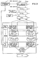
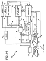
- FIG. 14 represents the block diagram of the main functions used in a particular embodiment.
- the equipment 20 can be produced with different sensors depending on the applications.
- the sensor used in this application is a strip of 2048 integrated photodiodes of the type manufactured by RETICON that allows the complete acquisition of a line of 2048 bits.
- a sensor 21 scans the reference module 22 carried by a support 23 and a sensor 24 scans the module to be examined 25 carried by an adjustable support 26. These sensors respectively develop I ref and exa , and are under the control of the clock 27.
- the reference module and the module to be examined are cropped beforehand using markers or markers prior to the inspection and sorting operation, properly speaking, or using equipment different from that shown. (of the mask alignment device type) or with the equipment shown.
- the module to be examined 25 is conveyed and automatically placed on its support, this operation ensures pre-alignment.
- the program placed in the computer 28 controls the motors 30, 30 and 31 for cropping in X, Y and 8 of the module 25 through the lines 32, 33 and 34, so that the marks arranged on the modules 22 and 25 can be analyzed .
- the support 23 is controlled synchronously by the motor 35 for the displacement in Y.
- the analog signals representative of I ref and of I exa from the sensors 21 and 24 are transmitted respectively by the bus 36 to a threshold detection block 37 where they are analyzed.
- Block 37 establishes the intensity histograms of I exa (gray distribution) and communicates them by bus 38 to the computer 28 which determines the threshold N TH of the image l exa .
- This value is then displayed by bus 39 at the input of block 40, which also receives analog signals from the sensors by bus 36.
- the images I exa and I ref are thresholded, each point image has the binary value 0 or 1.
- the binary images obtained referenced I REF and I EXA are transmitted by the bus 41 to the cropping calculation unit 42 which cropped I REF and I EXA , for example with the method described above above (1.4).
- the threshold value can be determined once and for all and this value permanently displayed in block 40 for all modules to consider from this family.
- the useful elements are transmitted by the bus 43 to the computer 28 which calculates the displacements in X, Y and 0 to be controlled.
- IREF can be contained in a memory of four million bits (see FIG. 3) which are addressed by a counter of 22 bits, under the control of the clock 27.
- a generator of configurations of the Gerber type can directly supply this representative electronic image, for example of the metallization mask. This electronic image is cropped, if necessary under the same conditions as above.
- the processing unit 43 then receives by the bus 44 electronic images I REF and I EXA perfectly framed.
- This unit comprises a memory 45 which is previously loaded by the data tables No. 1 and No. 2, that is to say which contains for each square the dimensional tolerance and the rejection criteria.
- This unit performs all the operations mentioned in step (1.5): adjustment to the dimensional tolerances of I REF , comparison between adjusted IREF and I EXA ' development of images of defects and analysis of said defects in view of the rejection criteria. It provides the computer with the elements of good / rejection decision by bus 46.
- This unit is driven by the clock 27, which also controls a double counter 47 of 22 bits.
- This double counter is wired so as to take account of the delay necessary for the output of the data relating to the adjustment to tolerances (carried out before the comparison operation) and the output of the data relating to the analysis of the defects in view of the criteria. rejection (performed after the comparison operation).
- This counter may or may not be an integral part of the processing unit.
- the content of this counter is the binary representation in X and in Y of the point of I ExA being analyzed. It suffices to count the number of clock pulses for each line to determine the address in X- (which corresponds to one of the 2048 diodes) and the number of end of line pulses (every 2048 pulses) to determine the address in Y.
- the seven most significant bits (among eleven) of the address in X and the seven bits (among the eleven) of most significant of the address in Y are combined to form an address, this address corresponds to a square, and at this address we find the corresponding data which define the dimensional tolerance and the rejection criterion for this square.
- This processing unit and the counter therefore make it possible to adjust the dimensional tolerance and rejection criteria in real time as a function of the X and Y coordinates of the points analyzed of the module to be examined, therefore associating with each pixel of I EXA ' the corresponding pixel of IREF and the data contained in the memory which correspond to it.
- the contents of memory 45 can be loaded either manually or automatically from this equipment during a preliminary step.
- the processing unit 43 is detailed in FIG. 15. It comprises the memory 45 which has been previously loaded with the data tables No: 1 and No. 2 and the counter 47 which makes it possible to associate with each pixel analyzed the data corresponding to the square that contains it. It also includes the various blocks for adjusting to dimensional tolerances for comparison and for analyzing faults.
- the processing principle is as follows: I EXA and I REF arrive via bus 44, ExA is adjusted to the minimum and maximum dimensional tolerances in blocks 48 and 49 respectively to provide ( I REF) mln and ( I REF) max ⁇ These images are compared with IExA ( previously delayed in the delay line 50) in the comparison circuits 51A and 51 B.
- the images of the resulting faults of the genus "lack" and of the genus “extension” are analyzed in the blocks of 52A and 52B fault analysis.
- the results of the analyzes are available on the buses 53A and 53B, then through the OR circuit 54 on the bus 46 which is connected to the computer 28.
- the adjustment blocks 48 and 49 include decoding circuits which are connected to the memory by the buses 55 and 56 to adjust the sizes of erosion and expansion, variable by definition.
- the fault analysis blocks 52A and 52B also include decoding circuits which are connected to the memory by the buses 57 and 58 respectively to adjust the rejection criteria, which are variable by definition.
- the constituent circuits of the counter and of the adjustment and analysis blocks are controlled by the clock 27.
- the double counter 47 includes the appropriate delay circuits (not shown).
- FIG. 16 represents a structuring element 59 of circular shape sampled according to a square frame and developed around a central pixel referenced 55.
- a pixel referenced ij means that its coordinate is i along the X axis and j along the axis of Y).
- the structuring element 59 is in fact constituted by the central pixel 55, and by four crowns referenced C1, C2, C3 and C4, the pixels belonging to the same crown are identified by the same distinctive sign.
- a pixel is represented by a point in FIG. 16, it should be understood that with a photodiodes array, used as a sensor, the exact representation would have been a square of 12.5 ⁇ of side centered on this pixel. With other sensors, this point representation can be exact.
- the circuit described in FIG. 17 is advantageous because the more the number of crowns increases, the more the structuring element approaches the circle.
- FIG. 17 The block for adjustment to the minimum tolerances which bears the reference 48 in FIG. 15 is detailed in FIG. 17.
- This block ensures the erosion operation with the structuring element shown in FIG. 16. It includes nine shift registers RD1 to RD9 of 2048 bits fed sequentially. These registers store part of the I REF image. Each of these registers drives a nine-bit shift register with parallel outputs. Either nine registers RD10 to RD18 with nine bits are used to make the structuring element of FIG. 16 which develops over nine lines and nine columns. At a given instant, while the image is loaded in the register RD1 to RD9, the numbers of the pixels loaded in the cells of the registers RD10 to RD18 are shown in FIG. 17.
- the cells whose content is involved in the definition of l structuring element 59 are connected to one of the four circuits 60 to 63 according to the crown of which the pixel is a part.
- the crown C4 comprises the pixels with the following numbers: 14, 15, 16, 23, 27, 32, 38, 41, 49, 51, 59, 61, 69, 72, 78 , 83, 87, 94, 95, 96.
- the outputs of the cells bearing these numbers are therefore connected to the inputs of the AND gate 60.
- the same is done for the three other rings C3, C2 and C1 which correspond respectively to the AND circuits 61, 62 and 63.
- the outputs of AND circuits 60 to 63 are respectively connected to OR circuits 64 to 67.
- Each of these circuits is controlled by a decoding circuit which is connected by bus 55 to data table No. 1 contained in memory 45 (figure -15).
- the decoding circuit 68 applies a "1" to the OR circuit corresponding to a crown that one does not want to put into action.
- the truth table of the decoding circuit is as follows:
- the block 49 is shown in FIG. 18, it can be deduced very simply from the block 48, by introducing an inverter 70 (to obtain (I REF ) °), then by performing a complementation of the final signal by the inverter 71. At d In other words, it suffices to add two inverters: one at the input and one at the output of block 48 to obtain block 49.
- All the shift registers are controlled by the clock 27 as is known.
- the reference signal I REF after erosion and expansion is compared with I EXA in a comparison circuit 51.
- FIG. 19 shows an example of a circuit 51 capable of carrying out the operation (SIGNAL A or SIGNAL B) OR EXC.
- SIGNAL B between the SIGNAL A and SIGNAL B input signals, which is the comparison operation mentioned as one of the operations in step 5.
- the circuit 51 includes an OR circuit 72 which receives the signal on the one hand A previously inverted in the inverter 73 and the signal B. The resulting signal is again inverted in the inverter 74. The output signal is therefore: this expression can also be written:
- comparison block 51 will be referenced 51A.
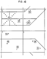
- FIG. 20 shows an analysis window 75 of 15 ⁇ 15 pixels which has four axes of symmetry (0, 45, 90 and 135 °).
- the overall shape is that of an eight-pointed star. All the pixels inside this star are taken into consideration (not all of them are shown in Figure 20).
- the pixels are referenced by their coordinates in X and in Y as it appears clearly in the figure.
- the central pixel therefore has the coordinates 1111.
- the size and shape of the analysis window depend on the application, in particular the size of the maximum permissible defect.
- Around the central pixel 111 which is by definition of the pixel being analyzed, an arbitrary defect has been shown which bears the reference 76.
- the horizontal and vertical projections of this defect are 50 p and 25 p.
- the projections are calculated from the activated photodiodes, therefore squares of 12.5 ⁇ side, schematically represented by pixels.
- the central pixel is arbitrarily considered to be part of the projection P-.
- FIG. 21 also shows the data extracted from the data table No. 1 relating to the square which contains the central pixel.
- FIG. 22 schematically represents the various circuits which make up the block 52A for analyzing faults with regard to the rejection criteria. It has two main functions: calculation of the projections of the fault in directions 8 and 8 + 90 °, and comparison with the rejection criteria which correspond to the maximum admissible size of the fault.
- the signal 78 which arrives at block 52A is therefore the signal representative of the image of faults of the "lack" type.
- a first circuit 79 composed in particular of shift registers with parallel outputs will allow access at any time to the content (0 or 1) of the cells of these registers corresponding to the desired pixels of window 75, distinguished by their coordinate. This circuit 79 is described in detail in FIG. 23. At the output of this circuit 79 are available all the pixels (in binary form) of the analysis window, therefore corresponding to the coordinate positions 0111 to 2111.
- the circuit 80A calculates the projection of the fault in the 0 ° direction.
- the binary value displayed on lines L01 to L15 is representative of the length of the fault.
- This circuit 80A is described in detail in FIG. 23. It will be recalled that the rejection criteria comprise two terms (L min -A and X% L min ) for the vertical projection and a term (k L min ) for the horizontal projection of the fault (see Figure 21), the role of circuits 81 is therefore, after decoding of the two directions in question (for example 0 ° and 90 °), to ensure that the dimensions of the fault in these two directions are acceptable.
- the circuits 81 are controlled from a demultiplexer 82 which receives its information from the memory 45 by the bus 57, according to a truth table which will be described below. Each circuit 81 therefore has two outputs.
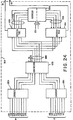
- the circuit 81A is described in detail in FIG. 24.
- the information available on the two lines of each circuit 81 is representative of the acceptable character or not of the projection of the fault according to the direction in question.
- This information is transmitted to a multiplexer 83 which, according to the value of 8, selects from the eight possible couples, the two couples which correspond to the direction of the driver and its perpendicular direction since the rejection criteria contain three terms, it is understood that only three values (1 horizontal projection and 2 vertical projections) are useful.
- the multiplexer 83 there are three values on the three lines W1, W2 and W3.
- Circuit ET 84 ensures that if the vertical projection of the fault is greater than X% L min and its horizontal projection is greater than k L min , the fault must lead to rejection (W4 at level 1).
- the line W1 is high (W1 at level 1) when the vertical projection is greater than L min -A.
- Lines W1, W4 and W5 are connected to an OR circuit 85, if only one of these three lines is high, line 53A is high, the fault is unacceptable and the module rejected.
- Line W5 comes from lines L15, M15, U15 and V15 which, as will be seen below, are high as soon as at least one of the two projections in the directions in question is greater than the dimension of the analysis window (15 pixels).
- the OR circuit 86 receives the couple of lines L15 and M15,
- the OR circuit 87 receives the couple U15 and V15, and the multiplexer 88 controlled by the direction of the conductor 6 selects the correct torque.
- block 52A The operation of block 52A will be better understood using the detailed description of the circuits shown in FIGS. 23 and 24.
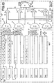
- block 79 is shown which is used for storing the analysis window.
- This block includes 21 shift registers of 2048 bits referenced RD01 to RD21, since the analysis window 75 expands over 21 lines (between pixels 0111 and 2111). These shift registers feed in cascade.
- Each register such as RD01 is linked to a 21-bit shift register (corresponding to the 21 columns of the analysis window) referenced RD01A.
- This register is of the parallel output type, that is to say that the content of each cell is accessible.
- the register RD11A contains all the pixels of the eleventh line, that is to say the pixels 1101 to 1121, all these pixels are used at least once to constitute the analysis window.
- the defect 76 of FIGS. 20 and 21 is characterized in that the pixels bearing the coordinates 1011, 1110, 1111, 1112 and 1113 have the binary value 1.
- circuits 80 The purpose of circuits 80 is to calculate the lengths of the fault.
- circuits 80A and 80B respectively calculate the dimensions of the fault in the directions 0 and 90 °, that is to say the horizontal and vertical projections of the fault 76 chosen by way of example. As soon as fault 76 fully enters the analysis window, the values of its exact projections are available on lines L01 to L15.
- Circuit 80A comprises a series of 15 OR circuits referenced 89 to 103, provided with 15 inputs.
- the OR gate 89 corresponds to all the pixels of the first column of the analysis window 75 in the 0 ° direction, that is to say the pixels referenced XX01 with XX varying from 04 to 18, and so on for all OR gates, OR gate 103 summing the pixels of the fifteenth column, that is to say the pixels XX18 with XX varying from 04 to 18. From the wiring point of view, or understands that the inputs of the gate OR 89 are connected to the outputs of the cells bearing the corresponding numbers, for example the first input 0404 is connected to the output of the fourth cell of RD04. We do the same for all OR doors of 80A. The construction of circuits 80B, 80C and 80D is easily deduced therefrom.
- the outputs of the OR gates are connected to AND gates as shown in FIG. 23.
- the outputs of the AND gates are referenced L01 to L15, the state of these outputs indicates the length of the fault according to the direction considered, relative to the central line L08 which is representative of the central pixel analyzed.
- the analysis window 75 is centered on the pixel 1111 of defect 76, only four OR gates have an output equal to 1, it is gates 95, 96, 97 and 98 which correspond to 7 °, 8 °, 9 ° and 10 ° window columns for which there is at least one pixel of value 1.
- Line L08 is at level 1 as soon as the central pixel analyzed is a pixel corresponding to a fault.
- the number of lines which are at the high level on either side of line L08 allows the immediate determination of the projection of the fault (in multiples of 12.5 p).
- the failure to default imposes "0" on all lines from the date of failure.
- the defect 76 does not extend to the sixth column, the OR gate 94 which corresponds to the pixels of this column receives only 0s on its inputs and therefore displays a 0 on the AND gate which follows it, the 0 is transmitted in cascade on all AND gates, so that lines L06 to L01 are at low level (0).
- An ET 104 gate plays a special role.
- Line L01 is also applied to it.
- L15 will be at level 1 when the defect is greater than or equal to the dimension of the analysis window (15 pixels), in this case the line L15 indicates that the projection of the defect is larger than the window analysis and that the module should be rejected.
- circuits 80B, 80C and 80D operate identically, and their outputs are referenced M01 to M15, N01 to N15 and Q01 to 015 respectively.
- the circuits 80A to 80D operate continuously and the projections in the four directions are available at all times. For example, when the analysis window is centered on the central pixel 1111, the circuit 80A which measures the horizontal projection (in the direction 0 °) of the defect 76 provides the value 50 ⁇ , the circuit 80B which measures the vertical projection ( in 90 ° direction) provides the value 25 p.
- the projections of the fault along directions 45 ° and 135 ° are respectively available on lines N01 to N15 and 001 to Q15, but are irrelevant in this case, since the direction direction of conductor 77 is 0 °.
- the projections are then quantified, this is the role of the encoders 105A and 106A. As output we therefore have the binary value corresponding to the value of the projection.
- the encoders can be EPROM memories of the MM 2708 type.
- the P- and P + projections are applied to the "addresses" inputs and the binary value is available on the "data" outputs.
- the transfer function of the 105A and 106A encoders is as follows:
- the central pixel being part as we have seen of P-, the maximum value of P + is 0111 while the maximum value of P - is 1000.
- the first encoder 105A which corresponds to P - provides the binary value 0010 while the encoder 106A which corresponds to P + also provides the binary value 0010.
- the binary value 0000 represents the absence of a fault
- the value 0001 a fault reduced to one pixel
- the data is supplied from the bus 82A (developed in the demultiplexer 82), to the double encoder circuit 109A, which displays the rejection criteria in binary form on the two comparators 110A and 111A.
- circuit 81A only one rejection criterion exists, also the encoder 109A displays 1111 on the comparator 111A by the bus 113A which also receives the projection P (1000) on its other inputs, the output R2 is therefore at level "0".
- the outputs T1 (which corresponds to the criterion X% L min ) and T2 (which corresponds to the criterion L min -A) are also at level 0.
- the circuits 81C and 81D which correspond to projections in directions not taken into account, have their respective outputs U1, U2 and V1, V2 forced to level 0 from the bus commands 82C and 82D coming from the demultiplexer 82, anyway these outputs will not be taken into account (in the example of fault 76) by the multiplexer 83, as will be explained below.
- This demultiplexer is shown in FIG. 22. It is controlled from the bus 57 which contains the data ⁇ , L min -A, X% L min , k L min . Depending on the value of ⁇ , the rejection criteria are directed to the appropriate circuits according to the following transfer table:
- the line W1 is at level 1 (this means that the vertical projection of the fault is greater than the rejection criterion L min -A) or that the line W4 is at level 1 (this means that the vertical projection of the fault is greater than kL min and that its horizontal projection is greater than KL min ) or finally that W5 is at level 1.
- Line W5 results through the multiplexer 88 from lines L15, M15, N15 and Q15 which we know to be at a high level as soon as the fault reaches, in the direction involved, the size of the analysis window.
- the fault analysis block 52B is identical in structure and operation to block 52A. Only the rejection criteria contained in the data table No. 2, correspond as we have seen to the interconductive space and to the direction 8 'of this space.
- the lines 53A and 53B are connected to an OR gate, which brings together the information from the fault analysis blocks 52A and 52B, the final information is processed by the computer.
Landscapes
- Engineering & Computer Science (AREA)
- Physics & Mathematics (AREA)
- General Physics & Mathematics (AREA)
- Computer Vision & Pattern Recognition (AREA)
- Quality & Reliability (AREA)
- Electromagnetism (AREA)
- Toxicology (AREA)
- General Engineering & Computer Science (AREA)
- Health & Medical Sciences (AREA)
- Theoretical Computer Science (AREA)
- Image Processing (AREA)
- Investigating Materials By The Use Of Optical Means Adapted For Particular Applications (AREA)
- Length Measuring Devices By Optical Means (AREA)
- Preparing Plates And Mask In Photomechanical Process (AREA)
- Testing Or Measuring Of Semiconductors Or The Like (AREA)
- Image Analysis (AREA)
Claims (25)


Priority Applications (4)
| Application Number | Priority Date | Filing Date | Title |
|---|---|---|---|
| DE8080430030T DE3070721D1 (en) | 1980-12-18 | 1980-12-18 | Process for inspecting and automatically classifying objects presenting configurations with dimensional tolerances and variable rejecting criteria depending on placement, apparatus and circuits therefor |
| EP80430030A EP0054596B1 (de) | 1980-12-18 | 1980-12-18 | Verfahren für die Inspektion und die automatische Sortierung von Objekten, die Konfigurationen mit dimensionellen Toleranzen aufweisen und platzabhängige Kriterien für die Verwerfung, Anlage und Schaltung dafür |
| JP56159541A JPS5951135B2 (ja) | 1980-12-18 | 1981-10-08 | 物体検査装置 |
| US06/329,892 US4481664A (en) | 1980-12-18 | 1981-12-11 | Process for inspecting objects showing patterns with dimensional tolerances and reject criteria varying with the locations of said patterns and apparatus and circuits for carrying out said process |
Applications Claiming Priority (1)
| Application Number | Priority Date | Filing Date | Title |
|---|---|---|---|
| EP80430030A EP0054596B1 (de) | 1980-12-18 | 1980-12-18 | Verfahren für die Inspektion und die automatische Sortierung von Objekten, die Konfigurationen mit dimensionellen Toleranzen aufweisen und platzabhängige Kriterien für die Verwerfung, Anlage und Schaltung dafür |
Publications (2)
| Publication Number | Publication Date |
|---|---|
| EP0054596A1 EP0054596A1 (de) | 1982-06-30 |
| EP0054596B1 true EP0054596B1 (de) | 1985-05-29 |
Family
ID=8187427
Family Applications (1)
| Application Number | Title | Priority Date | Filing Date |
|---|---|---|---|
| EP80430030A Expired EP0054596B1 (de) | 1980-12-18 | 1980-12-18 | Verfahren für die Inspektion und die automatische Sortierung von Objekten, die Konfigurationen mit dimensionellen Toleranzen aufweisen und platzabhängige Kriterien für die Verwerfung, Anlage und Schaltung dafür |
Country Status (4)
| Country | Link |
|---|---|
| US (1) | US4481664A (de) |
| EP (1) | EP0054596B1 (de) |
| JP (1) | JPS5951135B2 (de) |
| DE (1) | DE3070721D1 (de) |
Families Citing this family (79)
| Publication number | Priority date | Publication date | Assignee | Title |
|---|---|---|---|---|
| US4590607A (en) * | 1982-09-17 | 1986-05-20 | Environmental Research Institute Of Michigan | Image correspondence techniques using serial neighborhood processing |
| GB2129546B (en) * | 1982-11-02 | 1985-09-25 | Cambridge Instr Ltd | Image comparison |
| GB2129547B (en) * | 1982-11-02 | 1986-05-21 | Cambridge Instr Ltd | Reticle inspection |
| DE3475106D1 (en) * | 1983-04-15 | 1988-12-15 | Hitachi Ltd | Method and apparatus for detecting defects of printed circuit patterns |
| JPS6021523A (ja) * | 1983-07-15 | 1985-02-02 | Toshiba Corp | マスク欠陥検査方法 |
| JPH061370B2 (ja) * | 1983-11-24 | 1994-01-05 | 株式会社東芝 | マスク欠陥検査装置 |
| DE3377934D1 (en) * | 1983-12-28 | 1988-10-13 | Ibm | Process and equipment for the automatic alignment of an object in respect of a reference |
| DE3347645C1 (de) * | 1983-12-30 | 1985-10-10 | Dr.-Ing. Ludwig Pietzsch Gmbh & Co, 7505 Ettlingen | Verfahren und Einrichtung zum opto-elektronischen Pruefen eines Flaechenmusters an einem Objekt |
| GB2152658A (en) * | 1984-01-09 | 1985-08-07 | Philips Electronic Associated | Object sorting system |
| US4618938A (en) * | 1984-02-22 | 1986-10-21 | Kla Instruments Corporation | Method and apparatus for automatic wafer inspection |
| CA1229392A (en) * | 1984-02-28 | 1987-11-17 | Hirosato Yamane | Method and apparatus for detection of surface defects of hot metal body |
| JPS60230281A (ja) * | 1984-04-27 | 1985-11-15 | Fuji Electric Co Ltd | 文字識別装置 |
| US4853967A (en) * | 1984-06-29 | 1989-08-01 | International Business Machines Corporation | Method for automatic optical inspection analysis of integrated circuits |
| US4669466A (en) * | 1985-01-16 | 1987-06-02 | Lri L.P. | Method and apparatus for analysis and correction of abnormal refractive errors of the eye |
| US4776022A (en) * | 1985-04-09 | 1988-10-04 | Aoi Systems, Inc. | System for printed circuit board defect detection |
| JPS61251705A (ja) * | 1985-04-30 | 1986-11-08 | Sumitomo Metal Ind Ltd | パタ−ン検査方法及び装置 |
| IL79097A0 (en) * | 1985-06-17 | 1986-09-30 | Visionetics Corp | Automatic optical inspection of printed circuit boards |
| US4668982A (en) * | 1985-06-17 | 1987-05-26 | The Perkin-Elmer Corporation | Misregistration/distortion correction scheme |
| IL79098A0 (en) * | 1985-07-15 | 1986-09-30 | Visionetics Corp | Fine flaw detector for printed circuit boards |
| FR2587489B1 (fr) * | 1985-09-16 | 1988-07-08 | Bertin & Cie | Procede de controle optique automatique d'objets tels que des circuits integres |
| KR900007548B1 (ko) * | 1985-10-04 | 1990-10-15 | 다이닛뽕스쿠링세이소오 가부시키가이샤 | 패턴 마스킹 방법 및 그 장치 |
| US4928313A (en) * | 1985-10-25 | 1990-05-22 | Synthetic Vision Systems, Inc. | Method and system for automatically visually inspecting an article |
| US4942619A (en) * | 1986-01-20 | 1990-07-17 | Nikon Corporation | Pattern inspecting apparatus |
| US4771468A (en) * | 1986-04-17 | 1988-09-13 | International Business Machines Corporation | System for automatic inspection of periodic patterns |
| DE3786699T2 (de) * | 1986-05-10 | 1993-11-11 | Fujitsu Ltd | System zur Untersuchung von Mustern. |
| CA1284383C (en) * | 1986-08-04 | 1991-05-21 | Fmc Corporation | Computer integrated gaging system |
| US4918627A (en) * | 1986-08-04 | 1990-04-17 | Fmc Corporation | Computer integrated gaging system |
| US4796194A (en) * | 1986-08-20 | 1989-01-03 | Atherton Robert W | Real world modeling and control process |
| JPS63104185A (ja) * | 1986-10-22 | 1988-05-09 | Seiko Instr & Electronics Ltd | 画像の膨張・縮小変換回路 |
| US4949390A (en) * | 1987-04-16 | 1990-08-14 | Applied Vision Systems, Inc. | Interconnect verification using serial neighborhood processors |
| US5561696A (en) * | 1987-10-30 | 1996-10-01 | Hewlett-Packard Company | Method and apparatus for inspecting electrical connections |
| US4926452A (en) * | 1987-10-30 | 1990-05-15 | Four Pi Systems Corporation | Automated laminography system for inspection of electronics |
| US5081656A (en) * | 1987-10-30 | 1992-01-14 | Four Pi Systems Corporation | Automated laminography system for inspection of electronics |
| US5097492A (en) * | 1987-10-30 | 1992-03-17 | Four Pi Systems Corporation | Automated laminography system for inspection of electronics |
| US5621811A (en) * | 1987-10-30 | 1997-04-15 | Hewlett-Packard Co. | Learning method and apparatus for detecting and controlling solder defects |
| GB8811005D0 (en) * | 1988-05-10 | 1988-06-15 | Plessey Co Plc | Improvements in/relating to methods/registration |
| US5146510A (en) * | 1989-02-09 | 1992-09-08 | Philip Morris Incorporated | Methods and apparatus for optically determining the acceptability of products |
| US5046111A (en) * | 1989-02-09 | 1991-09-03 | Philip Morris Incorporated | Methods and apparatus for optically determining the acceptability of products |
| JP3132565B2 (ja) * | 1989-08-30 | 2001-02-05 | 株式会社日立製作所 | 欠陥検査方法及びその装置 |
| US5495424A (en) * | 1990-04-18 | 1996-02-27 | Matsushita Electric Industrial Co., Ltd. | Method and apparatus for inspecting solder portions |
| US5129009A (en) * | 1990-06-04 | 1992-07-07 | Motorola, Inc. | Method for automatic semiconductor wafer inspection |
| US5113565A (en) * | 1990-07-06 | 1992-05-19 | International Business Machines Corp. | Apparatus and method for inspection and alignment of semiconductor chips and conductive lead frames |
| JPH0786466B2 (ja) * | 1990-07-18 | 1995-09-20 | 大日本スクリーン製造株式会社 | プリント基板のパターン検査装置 |
| US5259012A (en) * | 1990-08-30 | 1993-11-02 | Four Pi Systems Corporation | Laminography system and method with electromagnetically directed multipath radiation source |
| US5231675A (en) * | 1990-08-31 | 1993-07-27 | The Boeing Company | Sheet metal inspection system and apparatus |
| US5214712A (en) * | 1990-09-11 | 1993-05-25 | Matsushita Electric Industrial Co., Ltd. | Pattern inspection system for inspecting defect of land pattern for through-hole on printed board |
| JP2500961B2 (ja) * | 1990-11-27 | 1996-05-29 | 大日本スクリーン製造株式会社 | プリント基板の座残り検査方法 |
| US5598345A (en) * | 1990-11-29 | 1997-01-28 | Matsushita Electric Industrial Co., Ltd. | Method and apparatus for inspecting solder portions |
| US5586058A (en) * | 1990-12-04 | 1996-12-17 | Orbot Instruments Ltd. | Apparatus and method for inspection of a patterned object by comparison thereof to a reference |
| US5237621A (en) * | 1991-08-08 | 1993-08-17 | Philip Morris Incorporated | Product appearance inspection methods and apparatus employing low variance filter |
| JP3265595B2 (ja) * | 1991-09-27 | 2002-03-11 | オムロン株式会社 | 画像処理方法およびその装置 |
| JP3445394B2 (ja) * | 1993-12-17 | 2003-09-08 | ゼロックス・コーポレーション | 少なくとも二つのイメージセクションの比較方法 |
| JP3986571B2 (ja) * | 1994-12-09 | 2007-10-03 | 日本テキサス・インスツルメンツ株式会社 | 歩留り予測装置とその方法 |
| US5583904A (en) * | 1995-04-11 | 1996-12-10 | Hewlett-Packard Co. | Continuous linear scan laminography system and method |
| US5687209A (en) * | 1995-04-11 | 1997-11-11 | Hewlett-Packard Co. | Automatic warp compensation for laminographic circuit board inspection |
| DE29510334U1 (de) * | 1995-06-26 | 1995-10-26 | AQS Dimensionale Meßtechnik GmbH, Hallein/Salzburg | System zur zweidimensionalen Vermessung planer Objekte |
| JP2885694B2 (ja) * | 1996-04-25 | 1999-04-26 | 山口日本電気株式会社 | 半導体基板表面の自動外観検査装置 |
| US5835634A (en) * | 1996-05-31 | 1998-11-10 | Adobe Systems Incorporated | Bitmap comparison apparatus and method using an outline mask and differently weighted bits |
| DE19636949A1 (de) * | 1996-09-11 | 1998-03-12 | Siemens Ag | Verfahren zur Detektion von Kanten in einem Bildsignal |
| US5978501A (en) * | 1997-01-03 | 1999-11-02 | International Business Machines Corporation | Adaptive inspection method and system |
| US6295374B1 (en) * | 1998-04-06 | 2001-09-25 | Integral Vision, Inc. | Method and system for detecting a flaw in a sample image |
| US6239276B1 (en) | 1998-06-22 | 2001-05-29 | Cytec Technology Corporation | Non-yellowing para-tertiary-alkyl phenyl substituted triazine and pyrimidine ultraviolet light absorbers |
| JP2002518489A (ja) | 1998-06-22 | 2002-06-25 | チバ スペシャルティ ケミカルズ ホールディング インコーポレーテッド | ポリ(トリスアリール−1,3,5−トリアジン=カルバマート)紫外光吸収剤 |
| US6297377B1 (en) | 1998-06-22 | 2001-10-02 | Cytec Technology Corporation | Benzocycle-substituted triazine and pyrimidine ultraviolet light absorbers |
| US6201850B1 (en) | 1999-01-26 | 2001-03-13 | Agilent Technologies, Inc. | Enhanced thickness calibration and shading correction for automatic X-ray inspection |
| US6859285B1 (en) | 1999-08-31 | 2005-02-22 | Og Technologies, Inc. | Optical observation device and method for observing articles at elevated temperatures |
| IL133313A (en) | 1999-12-05 | 2004-12-15 | Orbotech Ltd | Adaptive tolerance reference inspection system |
| US6488405B1 (en) * | 2000-03-08 | 2002-12-03 | Advanced Micro Devices, Inc. | Flip chip defect analysis using liquid crystal |
| US6867250B1 (en) | 2000-10-30 | 2005-03-15 | Cytec Technology Corp. | Non-yellowing ortho-dialkyl aryl substituted triazine ultraviolet light absorbers |
| US6492521B2 (en) | 2000-11-03 | 2002-12-10 | Cytec Technology Corp. | Hindered amine light stabilizers based on multi-functional carbonyl compounds and methods of making same |
| US6414155B1 (en) | 2000-11-03 | 2002-07-02 | Cytec Technology Corp. | Oligomeric hindered amine light stabilizers based on multi-functional carbonyl compounds and methods of making same |
| US6727300B2 (en) | 2000-11-03 | 2004-04-27 | Cytec Technology Corp. | Polymeric articles containing hindered amine light stabilizers based on multi-functional carbonyl compounds |
| US6545156B1 (en) | 2000-11-03 | 2003-04-08 | Cytec Technology Corp. | Oligomeric hindered amine light stabilizers based on multi-functional carbonyl compounds and methods of making same |
| US6996790B2 (en) * | 2003-01-30 | 2006-02-07 | Synopsys, Inc. | System and method for generating a two-dimensional yield map for a full layout |
| US7693336B2 (en) * | 2004-06-15 | 2010-04-06 | Fraudhalt Limited | Method and apparatus for determining if an optical disk originated from a valid source |
| US8106355B1 (en) | 2008-06-27 | 2012-01-31 | Kla-Tencor Corporation | Automated inspection using cell-cell subtraction perpendicular to stage motion direction |
| CN109431511B (zh) * | 2018-11-14 | 2021-09-24 | 南京航空航天大学 | 一种基于数字图像处理的人体背部脊柱侧弯脊柱轮廓特征曲线拟合方法 |
| CN112595234A (zh) * | 2021-01-04 | 2021-04-02 | 胜宏科技(惠州)股份有限公司 | 一种线路板复杂外形尺寸的检测方法 |
| CN114425524B (zh) * | 2021-12-20 | 2023-06-30 | 苏州镁伽科技有限公司 | 用于检测设备的收料控制方法、装置及检测设备 |
Family Cites Families (15)
| Publication number | Priority date | Publication date | Assignee | Title |
|---|---|---|---|---|
| US3546377A (en) * | 1968-06-12 | 1970-12-08 | Ovitron Corp | Video comparator using vidicons with delayed scanning |
| US3645626A (en) * | 1970-06-15 | 1972-02-29 | Ibm | Apparatus for detecting defects by optical scanning |
| US3955072A (en) * | 1971-03-22 | 1976-05-04 | Kasper Instruments, Inc. | Apparatus for the automatic alignment of two superimposed objects for example a semiconductor wafer and a transparent mask |
| JPS4934385A (de) * | 1972-07-28 | 1974-03-29 | ||
| JPS5427098B2 (de) * | 1972-09-11 | 1979-09-07 | ||
| US3909602A (en) * | 1973-09-27 | 1975-09-30 | California Inst Of Techn | Automatic visual inspection system for microelectronics |
| US3868508A (en) * | 1973-10-30 | 1975-02-25 | Westinghouse Electric Corp | Contactless infrared diagnostic test system |
| FR2321229A1 (fr) * | 1975-08-13 | 1977-03-11 | Cit Alcatel | Procede et appareillage pour controle automatique de graphisme |
| US3987244A (en) * | 1975-12-31 | 1976-10-19 | United Technologies Corporation | Programmable image processor |
| US4056716A (en) * | 1976-06-30 | 1977-11-01 | International Business Machines Corporation | Defect inspection of objects such as electronic circuits |
| US4247203A (en) * | 1978-04-03 | 1981-01-27 | Kla Instrument Corporation | Automatic photomask inspection system and apparatus |
| JPS5915381B2 (ja) * | 1978-10-16 | 1984-04-09 | 日本電信電話株式会社 | パタ−ン検査法 |
| JPS55142254A (en) * | 1979-04-25 | 1980-11-06 | Hitachi Ltd | Inspecting method for pattern of printed wiring board |
| DE2929846A1 (de) * | 1979-07-23 | 1981-03-12 | Siemens AG, 1000 Berlin und 8000 München | Opto-elektronisches pruefsystem zur automatischen beschaffenheitspruefung von leiterplatten, deren zwischenprodukte und druckwerkzeuge |
| US4269515A (en) * | 1979-08-07 | 1981-05-26 | Altman Associates, Inc. | Electro-optical system for inspecting printed circuit boards |
-
1980
- 1980-12-18 EP EP80430030A patent/EP0054596B1/de not_active Expired
- 1980-12-18 DE DE8080430030T patent/DE3070721D1/de not_active Expired
-
1981
- 1981-10-08 JP JP56159541A patent/JPS5951135B2/ja not_active Expired
- 1981-12-11 US US06/329,892 patent/US4481664A/en not_active Expired - Lifetime
Also Published As
| Publication number | Publication date |
|---|---|
| JPS57107046A (en) | 1982-07-03 |
| JPS5951135B2 (ja) | 1984-12-12 |
| EP0054596A1 (de) | 1982-06-30 |
| US4481664A (en) | 1984-11-06 |
| DE3070721D1 (en) | 1985-07-04 |
Similar Documents
| Publication | Publication Date | Title |
|---|---|---|
| EP0054596A1 (de) | Verfahren für die Inspektion und die automatische Sortierung von Objekten, die Konfigurationen mit dimensionellen Toleranzen aufweisen und platzabhängige Kriterien für die Verwerfung, Anlage und Schaltung dafür | |
| EP0054598B1 (de) | Verfahren zum Untersuchen und automatischen Sortieren von Objekten bestimmter Gestalt mit festen dimensionalen Toleranzen und Einrichtung zur Durchführung des Verfahrens | |
| BE1017547A6 (fr) | Compression d'images numeriques de documents scannes. | |
| EP0970367B1 (de) | Verfahren zur kontrolle der oberfläche einer laufenden materialbahn mit bildsegmentierung zur umgrenzung von defektbereichen | |
| FR2717925A1 (fr) | Procédé d'identification de défauts lors de l'inspection de surfaces structurées. | |
| EP0822515A1 (de) | Verfahren zur automatischen Segmentierung von numerischen Bildern und Vorrichtung zur Ausführung dieses Verfahrens | |
| FR2674340A1 (fr) | Procede pour detecter et classifier des particularites dans des images sonar. | |
| CA2047811A1 (fr) | Procede et dispositif de localisation en temps reel de contours rectilignes dans une image numerisee, notamment pour la reconnaissance de formes dans un traitement d'analyse de scene | |
| EP0627693A1 (de) | Vorrichtung zur Segmentierung von aus Texturen bestehenden Bildern und Segmentierungssysteme mit dieser Vorrichtung | |
| FR3030042A1 (fr) | Procede de detection de defaut sur une surface de pneumatique | |
| EP0970368B1 (de) | Verfahren zur kontrolle der oberfläche einer laufenden materialbahn mit vorklassifikation von ermittelten unregelmässigkeiten | |
| FR2788919A1 (fr) | Enlevement du bruit d'un signal obtenu par un systeme de generation d'image | |
| EP1129432B1 (de) | Verfahren zum vergleich von aus bildpunkten bestehenden gespeicherten bildern, die äquipotentielen mindestens einer integrierten schaltung darstellen | |
| EP3830789B1 (de) | Analyse von defekten von mindestens einem typ unter einer vielzahl von typen von defekten zwischen mindestens zwei proben | |
| FR2692059A1 (fr) | Procédé de comparaison de flots de données et dispositif de mise en Óoeuvre. | |
| FR2978274A1 (fr) | Procede de traitement differencie de zones d'une image | |
| EP0826960B1 (de) | Verfahren zur automatischen Erfassung von Fehlstellen in mechanischen Werkstücken mit komplizierter Geometrie | |
| FR2697930A1 (fr) | Procédé de réalisation d'une image de référence synthétisée pour l'inspection d'objets. | |
| JP2005300174A (ja) | 包装体の検査装置及び検査方法 | |
| WO2017001766A1 (fr) | Procédé de segmentation d'image | |
| Pillai et al. | Real-time Tablet Inspection using Computer Vision for Blister Packing Machines | |
| WO2026027717A1 (fr) | Procédé de segmentation d'une image numérique, dispositif électronique et application du procédé | |
| FR2681947A1 (fr) | Procede de classification automatique de defauts sur des micro-circuits. | |
| EP3189405B1 (de) | Verfahren zur bestimmung einer kontur mindestens eines bereichs auf einer matrizenoberfläche | |
| WO1998044338A1 (fr) | Procede d'inspection de surface d'une bande en defilement et d'analyse de la defectuosite de la bande |
Legal Events
| Date | Code | Title | Description |
|---|---|---|---|
| PUAI | Public reference made under article 153(3) epc to a published international application that has entered the european phase |
Free format text: ORIGINAL CODE: 0009012 |
|
| AK | Designated contracting states |
Designated state(s): DE FR GB IT |
|
| 17P | Request for examination filed |
Effective date: 19820713 |
|
| GRAA | (expected) grant |
Free format text: ORIGINAL CODE: 0009210 |
|
| AK | Designated contracting states |
Designated state(s): DE FR GB IT |
|
| PG25 | Lapsed in a contracting state [announced via postgrant information from national office to epo] |
Ref country code: IT Free format text: LAPSE BECAUSE OF FAILURE TO SUBMIT A TRANSLATION OF THE DESCRIPTION OR TO PAY THE FEE WITHIN THE PRESCRIBED TIME-LIMIT;WARNING: LAPSES OF ITALIAN PATENTS WITH EFFECTIVE DATE BEFORE 2007 MAY HAVE OCCURRED AT ANY TIME BEFORE 2007. THE CORRECT EFFECTIVE DATE MAY BE DIFFERENT FROM THE ONE RECORDED. Effective date: 19850529 |
|
| REF | Corresponds to: |
Ref document number: 3070721 Country of ref document: DE Date of ref document: 19850704 |
|
| PLBE | No opposition filed within time limit |
Free format text: ORIGINAL CODE: 0009261 |
|
| STAA | Information on the status of an ep patent application or granted ep patent |
Free format text: STATUS: NO OPPOSITION FILED WITHIN TIME LIMIT |
|
| 26N | No opposition filed | ||
| PGFP | Annual fee paid to national office [announced via postgrant information from national office to epo] |
Ref country code: DE Payment date: 19991118 Year of fee payment: 20 |
|
| PGFP | Annual fee paid to national office [announced via postgrant information from national office to epo] |
Ref country code: GB Payment date: 19991122 Year of fee payment: 20 |
|
| PGFP | Annual fee paid to national office [announced via postgrant information from national office to epo] |
Ref country code: FR Payment date: 19991217 Year of fee payment: 20 |
|
| PG25 | Lapsed in a contracting state [announced via postgrant information from national office to epo] |
Ref country code: GB Free format text: LAPSE BECAUSE OF EXPIRATION OF PROTECTION Effective date: 20001217 |
|
| REG | Reference to a national code |
Ref country code: GB Ref legal event code: PE20 Effective date: 20001217 |