EP0054710B1 - Procédé de positionnement et de contrôle d'une pièce munie de motifs, par exemple d'un masque pour la fabrication d'éléments semiconducteurs - Google Patents
Procédé de positionnement et de contrôle d'une pièce munie de motifs, par exemple d'un masque pour la fabrication d'éléments semiconducteurs Download PDFInfo
- Publication number
- EP0054710B1 EP0054710B1 EP19810109166 EP81109166A EP0054710B1 EP 0054710 B1 EP0054710 B1 EP 0054710B1 EP 19810109166 EP19810109166 EP 19810109166 EP 81109166 A EP81109166 A EP 81109166A EP 0054710 B1 EP0054710 B1 EP 0054710B1
- Authority
- EP
- European Patent Office
- Prior art keywords
- workpiece
- pattern
- region
- edge
- scanning
- Prior art date
- Legal status (The legal status is an assumption and is not a legal conclusion. Google has not performed a legal analysis and makes no representation as to the accuracy of the status listed.)
- Expired
Links
- 238000000034 method Methods 0.000 title claims description 26
- 238000004519 manufacturing process Methods 0.000 title claims description 9
- 239000004065 semiconductor Substances 0.000 title claims description 3
- 238000010894 electron beam technology Methods 0.000 claims description 29
- 238000012360 testing method Methods 0.000 claims description 19
- 239000000758 substrate Substances 0.000 claims description 15
- 239000000463 material Substances 0.000 claims description 10
- 238000001514 detection method Methods 0.000 claims description 4
- 229910052710 silicon Inorganic materials 0.000 claims description 2
- 239000010703 silicon Substances 0.000 claims description 2
- 239000012780 transparent material Substances 0.000 claims 1
- 239000011521 glass Substances 0.000 description 12
- 230000007547 defect Effects 0.000 description 6
- 238000010586 diagram Methods 0.000 description 4
- 238000005259 measurement Methods 0.000 description 4
- 238000012937 correction Methods 0.000 description 3
- 230000000694 effects Effects 0.000 description 3
- 230000003287 optical effect Effects 0.000 description 3
- 230000000295 complement effect Effects 0.000 description 2
- 230000003247 decreasing effect Effects 0.000 description 2
- 230000010354 integration Effects 0.000 description 2
- 239000002184 metal Substances 0.000 description 2
- XUIMIQQOPSSXEZ-UHFFFAOYSA-N Silicon Chemical compound [Si] XUIMIQQOPSSXEZ-UHFFFAOYSA-N 0.000 description 1
- 230000005540 biological transmission Effects 0.000 description 1
- 239000000969 carrier Substances 0.000 description 1
- 238000011156 evaluation Methods 0.000 description 1
- 238000007689 inspection Methods 0.000 description 1
- 238000003909 pattern recognition Methods 0.000 description 1
- 229920002120 photoresistant polymer Polymers 0.000 description 1
- 238000005070 sampling Methods 0.000 description 1
- 238000012216 screening Methods 0.000 description 1
- 230000001360 synchronised effect Effects 0.000 description 1
- XOLBLPGZBRYERU-UHFFFAOYSA-N tin dioxide Chemical compound O=[Sn]=O XOLBLPGZBRYERU-UHFFFAOYSA-N 0.000 description 1
- 229910001887 tin oxide Inorganic materials 0.000 description 1
- 230000000007 visual effect Effects 0.000 description 1
Images


Classifications
-
- G—PHYSICS
- G03—PHOTOGRAPHY; CINEMATOGRAPHY; ANALOGOUS TECHNIQUES USING WAVES OTHER THAN OPTICAL WAVES; ELECTROGRAPHY; HOLOGRAPHY
- G03F—PHOTOMECHANICAL PRODUCTION OF TEXTURED OR PATTERNED SURFACES, e.g. FOR PRINTING, FOR PROCESSING OF SEMICONDUCTOR DEVICES; MATERIALS THEREFOR; ORIGINALS THEREFOR; APPARATUS SPECIALLY ADAPTED THEREFOR
- G03F1/00—Originals for photomechanical production of textured or patterned surfaces, e.g., masks, photo-masks, reticles; Mask blanks or pellicles therefor; Containers specially adapted therefor; Preparation thereof
- G03F1/68—Preparation processes not covered by groups G03F1/20 - G03F1/50
- G03F1/82—Auxiliary processes, e.g. cleaning or inspecting
- G03F1/84—Inspecting
- G03F1/86—Inspecting by charged particle beam [CPB]
-
- H—ELECTRICITY
- H01—ELECTRIC ELEMENTS
- H01J—ELECTRIC DISCHARGE TUBES OR DISCHARGE LAMPS
- H01J37/00—Discharge tubes with provision for introducing objects or material to be exposed to the discharge, e.g. for the purpose of examination or processing thereof
- H01J37/30—Electron-beam or ion-beam tubes for localised treatment of objects
- H01J37/304—Controlling tubes by information coming from the objects or from the beam, e.g. correction signals
- H01J37/3045—Object or beam position registration
Definitions
- the invention has for its object to avoid the above-mentioned shortcomings of the previously usual methods for aligning and testing workpieces provided with samples and to show a method which, using the data used for the manufacture of the workpiece and the samples thereon, enables an independent accurate alignment and testing of the workpiece guaranteed and that is particularly suitable for masks with very fine and complex pattern structures.
- the invention uses in a known manner a controllable scanning beam and an evaluation circuit for the signals reflected or transmitted from the workpiece surface, e.g. B. secondary electrons, wherein the scanning beam is already deflected to align successively to different areas of the workpiece to be tested.
- the invention is characterized by the method described in the claims. According to the invention, irrespective of any rough alignment marks for a previous rough alignment of the workpiece, existing geometrical figures, such as edges or the like, of selected areas of the mask pattern, the position of which is known to one another by the data from the production of the pattern, as machine-scannable fine alignment marks used so that each field and each area of a field can be precisely located and measured in relation to the respective test position. It does not matter whether individual sample areas are uniform or different from one another, and any manufacturing errors or problems with the exact adherence to the feed steps have no influence on the alignment and test results. This is because the digitally stored data of the manufacturing process of the workpiece in question are used.
- the application of the method according to the invention therefore ensures a cost-effective one-hundred percent inspection of workpieces with a complex geometric pattern structure of finest screening.
- defects of a size of 1 diameter can be reliably detected when the electron beam covers a square area with a side length of approximately 1.5, so that it overlaps the previous scanning area by 0.75 to 1 in each axis direction.
- the use of a beam area which corresponds approximately to the minimum area of the defects to be determined, improves the performance of the system and avoids complex pattern recognition devices and programs, as are necessary for smaller beam areas.
- a particular advantage of the method according to the invention is that the position of detected errors is immediately available and can be registered without further analysis, since the addressing and scanning of the individual areas is carried out in accordance with the present description.
- An electron beam, a cathode beam or an optical beam in the visible or invisible range, such as infrared light or X-rays, can be used to carry out the method according to the invention.
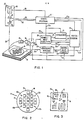
- the arrangement shown in Fig. 1 includes a table 10 adjustable in the X and Y directions, on which the workpiece 11 to be tested, e.g. a mask.
- the workpiece 11 consists of a substrate 12 with a number of coarse alignment marks 13a, 13b, 13c and 13d and a number of fields 14.
- the coarse alignment marks 13 are designed as crosses, but can also be in the form of a cross Angle, etc. can be shown.
- workpieces that are used as chip carriers or optically transparent masks made of glass with a layer of optically opaque materials, such as metal or photoresist, are also considered as workpieces.
- the masks can also be made of other materials, e.g. Silicon exist, which are transparent to infrared light.
- a substrate 12 made of glass is used, the pattern 15 of which is formed by thin metal films applied to the glass.
- each field consists of a number of different geometric metallized patterns 15 which, as mentioned, are applied to the substrate 12.
- the fields 14 are identical to one another.
- the alignment and checking of the individual fields described below does not require this.
- Each mask to be checked can. therefore have a variety of different patterns including the control test pattern.
- the 1 further includes an electron beam device 16, a beam controller 17, a detector 18, an amplifier 19, a threshold circuit 20, a comparator 21, a measurement circuit 22, a pattern-hold circuit 23, a digital controller 24 and a switch 25 for connecting the detector 18 and the amplifier 19 either to the comparator 21, the threshold circuit 20 or the measurement circuit 22.
- the actuation of the switch 25 is synchronized with the operations of the beam control 17 by means of a line 17a.
- the digital controller 24 is designed as a universal computer (processor) and contains all the necessary information and data relating to the mask to be checked, including all alignment marks and the shape and position of the individual patterns 15. Furthermore, the digital controller 24 generates the signals for operating the beam controller 17, which are a line 26 switches the electron beam source 27 on and off for generating the electron beam 28.
- the beam controller 17 further controls the deflection plates 31 and 32 for the electron beam 28 in a known manner via lines 29 and 30 and synchronizes the operations of the threshold value circuit 20, the comparator 21, the measurement circuit 22 and the pattern holding circuit via lines 17a and 17b. Circuit 23 and the switch 25. Finally, the digital control 24 also controls the respective position of the table 10 via a line 33.
- the mask to be tested is held on the table 10 by an appropriate clamping device, for example by means of a vacuum.
- a thin, conductive, grounded, transparent layer 53 is applied to the surface of the substrate 12, thereby ensuring that the electron beam neither charges the material forming the patterns 15a, 15b, etc., nor the substrate itself as it passes over the selected areas.
- a suitable material for this is, for example, tin oxide.
- Layer 53 (Fig. 2), however, is not required if the substrate is conductive or semiconductive, or if it is a beam with no charging effect, e.g. a beam of light.
- the switch 25 is set in such a way that the detector 18 and the amplifier 19 are connected to the threshold circuit 20 via the line 25b, and the digital controller 24, which acts as a processor, causes the beam controller 17 to switch on the electron beam 28, which the mask 11 and its fields 14 is able to record.
- the impact of the electron beam on the glass of the substrate 12 and the different patterns 15 on the substrate 12 causes both secondary electrons and backscattering electrons reflected from the mask.
- Each of the materials, e.g. Glass or the material forming the pattern emits different strengths of secondary electrons and backscattering electrons.
- the glass of the substrate 12 will emit secondary electrons of a certain, usually low strength, while the patterns emit secondary electrons of different, preferably higher, strength.
- the determination of the respective secondary electrons is therefore used in the following in the processes described, although the arrangement shown could also use backscattering electrons.
- the electron beam is now controlled for scanning over a selected field 14. This creates different strengths of secondary electrons, depending on whether the beam hits a glass or a sample surface. These secondary electrons are detected by the detector 18, which generates a corresponding signal proportional to the respective number of secondary electrons, which is amplified by the amplifier 19 and then transmitted to the threshold value circuit 20. As shown in FIG. 5, the threshold circuit 20 includes a pair of pattern hold circuits 34 and 35 and a voltage divider 36.
- the electron beam is first directed onto the glass surface of the substrate 12, and at the same time, the digital controller 24 sends a signal via a line 37 to the pattern holding circuit 34 for switching it on, and this signal ends after a predetermined time.
- the electron beam is then directed onto a pattern area, and a second signal reaches the pattern holding circuit 35 via a line 38.
- the output signals of the pattern-holding circuits 34 and 35 pass via lines 39 and 40 to the voltage divider 36, the output signals of which are fed to the comparator 21 via a line 41 and the provides a threshold voltage against the signals supplied to comparator 21 on line 25a.
- This threshold value is therefore dynamic and is determined by the average value of the different signal strengths as they arise when the secondary electrons are scanned from the glass surfaces and the pattern surfaces. This determination of a threshold value for the signal strength is particularly important if the signal determined on the basis of the secondary electrons is unstable or inconsistent, namely fluctuates as a result of density changes, geometric errors or the like. You can also use more than one threshold for certain applications. You can also periodically adapt the threshold value to changing beam currents or signal strengths, as can be caused by different irradiated objects, such as pattern thickness or density.
- the arrangement according to FIG. 1 can be equipped with an optical microscope in order to roughly align the workpiece 11 by means of visual observation of the alignment marks 13a, 13b, 13c and 13d.
- the information stored in the digital controller 24 is then used to switch on the electron beam device 16 and to control the movement of the table 10.
- the workpiece hereinafter referred to as mask 11
- the beam controller 17 now causes the beam 28 to sweep over the selected field 14 or a specific region thereof.
- each field up to a final predetermined test position can now be obtained by scanning certain patterns 15 of an area or partial area of the selected field 14.
- the selected area can be the same only for the purpose of alignment and from field to field, or it is a component of the field pattern itself, in which case the pattern may vary from field to field.
- the samples to be scanned for registration are predetermined in the same manner as the corresponding samples used to conduct the test, using any selected area of the field. An example of this is shown in FIG. 6, where three pattern areas according to FIG. 3 arranged in the upper left corner area of the field 14 are shown enlarged and are used as a selected area of this field in the following example.
- the switch 25 is now set such that the rated circuit 22 is connected to the detector 18 and the amplifier 19 via the line 25c.
- the digital control 24 then effects the control of the electron beam 28 via the beam control 17 in such a way that it scans selected edges of each of the patterns 15a, 15b and 15c and determines their position relative to the desired test position.
- the dimensioning circuit 22 effects a position correction in the beam control 17 via the pattern-holding circuit 23 and the line 23a, as a result of which the electron beam 28 is directed into such a position that with respect to the Movement range of the beam the entire selected field reaches the desired test position.
- an error amount is obtained which indicates the deviation of the sample image from the desired test position into which the selected area of the field is to be aligned.
- This amount of error is independent of any size error values.
- the beam is first guided to the left edge, that is to say in the horizontal direction, over the pattern 15, which is represented in FIG. 6 by the hatched area of the area 44. This scanning process generates secondary electrons both from the pattern and from the substrate glass surface, which are detected by the detector 18 and fed to the dimensioning circuit 22.
- the dimensioning circuit 22 contains a reversing circuit 50, an integration circuit 51 and a switch 52 which is actuated by the digital controller 24 via the line 22b. By closing the switch 52, the reversing circuit 50 is separated from the rated circuit 52.
- the switch 52 is opened so that the signal passes through the inverter 50.
- the electron beam is now moved along the edge of the pattern 15a.
- the area swept here has a certain width B and length L and is drawn as a hatched area representing the area 44.
- the signal sampled in this case is passed from the detector 18 via the line 25c to the dimensioning circuit 22, the inversion circuit reverses the input signal and feeds it to the integrator 51, the output signal of which is fed to the pattern-holding circuit 23 on line 22a.
- the detector 18 generates a square-wave voltage pulse 85 from time t1 to time t2 for transmission via line 25c.
- This square-wave voltage pulse is converted into a voltage line with increasing voltage value by means of the measuring circuit 22, and this signal appears on line 22a. It begins at time t1 and is continuously increased above a basic value 80 (see FIG. 8) until the square-wave voltage pulse 85 ends at time t2.
- the height h by which the voltage line 86 rises is proportional to the total number of secondary electrons emitted by the scanned area 44. A percentage of the secondary electrons detected by the detector 18 come from the substrate glass surface and the rest from the sample surface.
- the electron beam 28 is switched off, and the dimensioning circuit 22 is reset by switching the switch 52.
- the beam is now pivoted to the right by an amount corresponding to the width of the pattern 15a, so that the area 45 can now be swept along the right edge of the pattern 15.
- This area 45 also has the width B and Length L.
- the secondary electrons are registered in the same way by the detector 18 and transmitted from the time t3 to the time t4 as a square-wave voltage pulse 87 via the line 25c to the dimensioning circuit 22.
- the switch 25 is in the position in which the reversing circuit 50 is switched off, this signal is fed directly to the integrator 51 bypassing the reversing circuit 50.
- the output signal of the rated circuit 22 is characterized by the voltage line 88 with a decreasing voltage value. If, as shown, this voltage line reaches the basic value 80 at time t4, this shows that the area 44 overlaps exactly the same amount of the pattern 15a as the area 45.
- the difference value can be evaluated as an indication of the correction value, which must be taken into account in order to achieve the desired test position. This case is explained below with the help of FIGS. 9 and 10 explained.
- scan areas 100 and 101 overlapping the pattern 102 are shown, the scan area 100 overlapping the pattern 102 by a larger amount than the scan area 101.
- the scan of the area 100 results in a square-wave voltage pulse from time t1 to Time t2, which is converted by means of the measurement circuit 22 in a voltage line 96 with increasing voltage value, starting at the basic value 94. Since the scanning area 100 covers a larger area of the pattern 102, the number of secondary electrons determined is correspondingly higher.
- the electron beam then sweeps over the scanning area 101, and as a result of the smaller overlap area thereof, the square-wave voltage pulse 97 is of a lower height than the square-wave voltage pulse 95 in the time interval from t3 to t4. but ends at a height denoted by 99 above the basic value 94.
- This value is proportional to the deviation K of the edge of the pattern 102 from the center line of the scanning beams, and this deviation value is now transmitted via line 23a to the beam controller 17 in order to correspondingly increase the beam direction correct.
- the information obtained can be transmitted simultaneously to the digital controller 24, which in turn sends corresponding control signals to the beam controller 17.
- the position of the scanning beams with respect to the pattern in the direction from left to right can be determined . If desired, this process can be repeated using another left area 46 of the pattern 15c and a right area 47 of the pattern 15b. If the area in question, as part of the entire field, has been adjusted in the direction from left to right, i.e. horizontally, to the desired position, the same procedure is repeated with respect to the direction from top to bottom, i.e. in the vertical direction .
- the electron beam is first guided over the area 48 in the upper part of the pattern 15a and then over the area 49 in the lower part of the pattern 15c, as shown in FIG. 6.
- the areas are of equal width and length, so that the resulting signals are proportional to the amount of overlap of the beam and patterns.
- the information determined in this case is in turn fed to the beam controller 17 in order to carry out a corresponding correction in the vertical direction in order to achieve the desired test position.
- the switch 25 is first switched back so that the rated circuit 22 is switched off and the comparator 21 is connected to the detector 18 and the amplifier 19.
- a voltage value corresponding to the previously determined threshold value is now supplied from the threshold value circuit 20 to the comparator 21 via the line 41.
- the digital controller 24, which contains all the data about the patterns to be tested, causes the electron beam 28 to be switched on to scan the patterns 15a, 15b and 15c within the area to be tested.
- the beam is of uniform size and only travels over those areas of the areas in which there are patterns.
- the comparator 21 delivers a signal to the digital controller 24 for the respective secondary electron current of each sampled pattern as often as the sampling signal falls below the threshold voltage, the corresponding coordinates of the beam for indicating “missing pattern” being registered at this point.
- the beam is stepped through those areas where no patterns or pattern-like materials are expected.
- the secondary electron current is measured and a signal is supplied to the digital controller 24 whenever the current exceeds the specified threshold value.
- the corresponding coordinate values of the beam are also registered, indicating that a pattern or pattern-like material has been found at this point, although none was expected here.
- This edge region 150 is represented in FIG. 7 by the dashed lines 151 and 152 (pattern 15a). Accordingly, the pattern 15a is scanned over the area of the hatched area within the dashed line 151 and the scanning of the surrounding areas outside the dashed line 152. The same applies to the patterns 15b and 15c. Of course, if one dispenses with these edge areas 150, the circuit and program memory expenditure is considerably low.
- Each area forming a partial area of a field is scanned three times in succession: the first time with a deflection over the edges of the expected patterns in the area in question in order to immediately register the position of the area in question; the second time with a deflection over all parts of the area in question from which a certain signal strength is expected, and the third time with a deflection of the beam over all other parts of the area from which the other signal strength is expected.
- the last two scans are therefore essentially complementary within one area, but differ from one area to the next. All three scanning processes are each defined by the stored information about the existing patterns on the workpiece to be tested, usually using the numerical data tables that were already used to manufacture the workpiece.
- the scanning of the complementary areas described above is expediently carried out by scanning successive individual rectangular areas, with predetermined coordinates for each beam position, so that in the event of a deviation from an expected reflection signal, the coordinates of the relevant error position are immediately available and can be registered for a subsequent repair.
- the use of rectangular or square, non-overlapping beam areas is known.
- the use of relatively large overlapping rectangular beam areas has the advantages of higher throughput, greater certainty in the detection of significant defects, less likelihood of erroneous identification of defects and sufficient signal strength.
Landscapes
- Chemical & Material Sciences (AREA)
- Analytical Chemistry (AREA)
- Physics & Mathematics (AREA)
- General Physics & Mathematics (AREA)
- Testing Or Measuring Of Semiconductors Or The Like (AREA)
- Length-Measuring Devices Using Wave Or Particle Radiation (AREA)
Claims (8)
Applications Claiming Priority (4)
| Application Number | Priority Date | Filing Date | Title |
|---|---|---|---|
| US06/218,322 US4357540A (en) | 1980-12-19 | 1980-12-19 | Semiconductor device array mask inspection method and apparatus |
| US218323 | 1980-12-19 | ||
| US218322 | 1980-12-19 | ||
| US06/218,323 US4365163A (en) | 1980-12-19 | 1980-12-19 | Pattern inspection tool - method and apparatus |
Publications (2)
| Publication Number | Publication Date |
|---|---|
| EP0054710A1 EP0054710A1 (fr) | 1982-06-30 |
| EP0054710B1 true EP0054710B1 (fr) | 1986-02-05 |
Family
ID=26912798
Family Applications (1)
| Application Number | Title | Priority Date | Filing Date |
|---|---|---|---|
| EP19810109166 Expired EP0054710B1 (fr) | 1980-12-19 | 1981-10-29 | Procédé de positionnement et de contrôle d'une pièce munie de motifs, par exemple d'un masque pour la fabrication d'éléments semiconducteurs |
Country Status (2)
| Country | Link |
|---|---|
| EP (1) | EP0054710B1 (fr) |
| DE (1) | DE3173738D1 (fr) |
Families Citing this family (3)
| Publication number | Priority date | Publication date | Assignee | Title |
|---|---|---|---|---|
| US4546260A (en) * | 1983-06-30 | 1985-10-08 | International Business Machines Corporation | Alignment technique |
| US4581537A (en) * | 1984-03-23 | 1986-04-08 | International Business Machines Corporation | Method for generating inspection patterns |
| US4705954A (en) * | 1984-09-04 | 1987-11-10 | Siemens Aktiengesellschaft | Method and apparatus for automatically positioning a particle beam |
Family Cites Families (3)
| Publication number | Priority date | Publication date | Assignee | Title |
|---|---|---|---|---|
| US3901814A (en) * | 1974-06-27 | 1975-08-26 | Ibm | Method and apparatus for detecting a registration mark on a target such as a semiconductor wafer |
| JPS5915381B2 (ja) * | 1978-10-16 | 1984-04-09 | 日本電信電話株式会社 | パタ−ン検査法 |
| JPS5572807A (en) * | 1978-11-27 | 1980-06-02 | Hitachi Ltd | Electron-beam mask check unit |
-
1981
- 1981-10-29 EP EP19810109166 patent/EP0054710B1/fr not_active Expired
- 1981-10-29 DE DE8181109166T patent/DE3173738D1/de not_active Expired
Also Published As
| Publication number | Publication date |
|---|---|
| DE3173738D1 (en) | 1986-03-20 |
| EP0054710A1 (fr) | 1982-06-30 |
Similar Documents
| Publication | Publication Date | Title |
|---|---|---|
| DE2810025C2 (fr) | ||
| EP1075642B1 (fr) | Appareil de mesure de cordonnées de position pour la mesure de structures sur un substrat transparent | |
| DE19825829C2 (de) | Verfahren zur Bestimmung des Abstandes P einer Kante eines Strukturelementes auf einem Substrat | |
| DE2222665A1 (de) | Verfahren und Vorrichtung zum Ausrichten von Elektronenprojektionssystemen | |
| DE3735154C2 (de) | Verfahren zum Erfassen der Lage einer auf einem Objekt vorgesehenen Marke | |
| DE2939044A1 (de) | Einrichtung fuer elektronenstrahllithographie | |
| EP0043863A1 (fr) | Procédé pour la compensation de l'effet de proximité dans les dispositifs de projection de rayonnement électronique | |
| DE2659247A1 (de) | Elektronenstrahlenbuendel benutzendes, lithografisches system | |
| DE3621045A1 (de) | Strahlerzeugende vorrichtung | |
| EP0003038B1 (fr) | Procédé de mesure des erreurs de positionnement en utilisant un système de faisceau électronique comme instrument de mesure | |
| DE3206374C2 (de) | Verfahren und Vorrichtung zum Eichen der Ablenkung eines aus geladenen Teilchen bestehenden Strahls | |
| DE4221080A1 (de) | Struktur und verfahren zum direkten eichen von justierungsmess-systemen fuer konkrete halbleiterwafer-prozesstopographie | |
| DE102008062928A1 (de) | Verfahren zum Ermitteln einer Reparaturform eines Defekts an oder in der Nähe einer Kante eines Substrats einer Photomaske | |
| DE19802848B4 (de) | Verfahren und Vorrichtung zum Testen eines Substrats | |
| EP0025036B1 (fr) | Procede pour la mise a point d'une image d'un masque sur une piece a usiner | |
| DE2502591C2 (de) | Verfahren und Vorrichtung zur Ermittlung einer Ausrichtmarkierung | |
| DE3410885A1 (de) | Fehlerkorrigierte korpuskularstrahllithographie | |
| DE1804646A1 (de) | Korpuskularstrahl-Bearbeitungsgeraet mit einem Objekttisch und Ablenkmitteln fuer den Strahl | |
| DE102007039982B3 (de) | Verfahren zur optischen Inspektion und Visualisierung der von scheibenförmigen Objekten gewonnenen optischen Messerwerte | |
| EP0176745A1 (fr) | Dispositif et procédé pour mesurer des longueurs dans un microscope corpusculaire à balayage | |
| DE2525235A1 (de) | Verfahren und anordnung zum feststellen einer ausrichtmarke auf einer auffangplatte, wie z.b. einem halbleiterplaettchen | |
| DE19817714B4 (de) | Verfahren zur Messung der Lage von Strukturen auf einer Maskenoberfläche | |
| DE3732149C2 (de) | Verfahren und Vorrichtung zum Charakterisieren einer Genauigkeitseigenschaft einer optischen Linse | |
| DE19544753C2 (de) | Elektronenstrahl-Schreibverfahren | |
| EP0054710B1 (fr) | Procédé de positionnement et de contrôle d'une pièce munie de motifs, par exemple d'un masque pour la fabrication d'éléments semiconducteurs |
Legal Events
| Date | Code | Title | Description |
|---|---|---|---|
| PUAI | Public reference made under article 153(3) epc to a published international application that has entered the european phase |
Free format text: ORIGINAL CODE: 0009012 |
|
| 17P | Request for examination filed |
Effective date: 19811029 |
|
| AK | Designated contracting states |
Designated state(s): DE FR GB |
|
| GRAA | (expected) grant |
Free format text: ORIGINAL CODE: 0009210 |
|
| AK | Designated contracting states |
Designated state(s): DE FR GB |
|
| ET | Fr: translation filed | ||
| REF | Corresponds to: |
Ref document number: 3173738 Country of ref document: DE Date of ref document: 19860320 |
|
| PLBE | No opposition filed within time limit |
Free format text: ORIGINAL CODE: 0009261 |
|
| STAA | Information on the status of an ep patent application or granted ep patent |
Free format text: STATUS: NO OPPOSITION FILED WITHIN TIME LIMIT |
|
| 26N | No opposition filed | ||
| PG25 | Lapsed in a contracting state [announced via postgrant information from national office to epo] |
Ref country code: GB Effective date: 19891029 |
|
| GBPC | Gb: european patent ceased through non-payment of renewal fee | ||
| PG25 | Lapsed in a contracting state [announced via postgrant information from national office to epo] |
Ref country code: FR Effective date: 19900629 |
|
| PG25 | Lapsed in a contracting state [announced via postgrant information from national office to epo] |
Ref country code: DE Effective date: 19900703 |
|
| REG | Reference to a national code |
Ref country code: FR Ref legal event code: ST |