EP0054738A2 - Method and apparatus for low-frequency noise suppression in the output signals of semiconducteur sensors - Google Patents
Method and apparatus for low-frequency noise suppression in the output signals of semiconducteur sensors Download PDFInfo
- Publication number
- EP0054738A2 EP0054738A2 EP81109458A EP81109458A EP0054738A2 EP 0054738 A2 EP0054738 A2 EP 0054738A2 EP 81109458 A EP81109458 A EP 81109458A EP 81109458 A EP81109458 A EP 81109458A EP 0054738 A2 EP0054738 A2 EP 0054738A2
- Authority
- EP
- European Patent Office
- Prior art keywords
- output signals
- low
- maximum
- minimum
- frequency noise
- Prior art date
- Legal status (The legal status is an assumption and is not a legal conclusion. Google has not performed a legal analysis and makes no representation as to the accuracy of the status listed.)
- Granted
Links
Images


Classifications
-
- H—ELECTRICITY
- H04—ELECTRIC COMMUNICATION TECHNIQUE
- H04N—PICTORIAL COMMUNICATION, e.g. TELEVISION
- H04N25/00—Circuitry of solid-state image sensors [SSIS]; Control thereof
- H04N25/60—Noise processing, e.g. detecting, correcting, reducing or removing noise
Definitions
- the signal curve of a clock period is such that a maximum value dependent on the brightness follows a minimum value independent of the brightness.
- the object of the present invention is to suppress this noise.
- the method according to the invention with the characterizing features of the main claim has the advantage that this essentially low-frequency noise component is largely suppressed.
- 1 represents the 1 represents the actual image area
- shift registers 2 and 3 transport the charges from the image area to the outputs in time with clock pulses supplied at 4 and 5.
- An amplifier 6, 7 is arranged at each of the outputs of the shift registers 2, 3, at the outputs 8 and 9 of which the signals, the course of which is shown schematically, can be removed.
- the output signals have the spectrum shown in FIG. 2, which comprises a baseband up to approximately 5 MHz at a sampling frequency of 10 MHz.
- this baseband is usually separated by a low-pass filter, so that a video signal corresponding to the spectral distribution denoted by 10 occurs.
- noise is superimposed on this signal, the spectral distribution of which roughly corresponds to curve 11.
- the spectrum of the signals present at 8 and 9 also includes a carrier at 10 MHz and its sidebands of t 5 MHz.
- the minimum and maximum values are separated from one another by threshold value circuits.
- the output signals of the threshold circuits 22 and 23 are fed to the inputs of a subtracting circuit 24. This ensures that only the difference between the maximum and minimum values is determined and is available as a video signal via the low-pass filter 25.
- the minimum and maximum values are separated by non-additive mixing circuits 26 and 27, which essentially consist of two transistors each, which are connected to a common load resistor via their emitters.
- the noise can also be suppressed by using the carrier band to obtain the video signal.
- the output signals are used for this routed via a bandpass 28, 29, the pass band of which ranges from 5 MHz to 15 MHz.
- Both carrier-frequency signals are fed to an envelope demodulator 30, the output signal of which is fed via an amplifier 31 and a low-pass filter 32 to the output 33 of the arrangement according to FIG. 6.
- the circuit according to FIG. 8a is supplied with the output signals of the sensor at points 8 and 9.
- the corresponding output circuits of the sensor are only shown schematically as generators 51 and 52 in FIG. 8a.
- the form of the signals supplied at 8 and 9 to the circuit arrangement according to FIG. 8a is shown in FIG. 8b in lines a1 and a2.
- the signals are read out correspondingly out of phase.
- the resulting pulse shape is shown schematically in FIG. 8b as a triangular voltage, the amplitude drawn upwards being given in the pulse interval in which no information is read out from the sensor, while the amplitude drawn downwards in FIG. 8b is given in each case read information corresponds.
- the signal shown in FIG. 8b, line a2 is based on an unexposed sensor, the level for maximum exposure (ws) is shown in dashed lines.
- further impedance converters consisting of the field effect transistors 67 and 68, are connected to these, whose load resistors are the resistors 69 and 70 and which are connected to the bases of the transistors 71 and 72, which in turn are emitter-coupled to one another and have a common emitter resistor 73.
- the transistors 71 and 72 act as a so-called NAM circuit (non-additive mixture). Of the voltages which are supplied to the bases of the transistors 71 and 72, that voltage is forwarded to the node 74 which has a more negative instantaneous value.
- the output voltages of the NAM circuits are now to be subtracted from one another. This takes place in an operational amplifier 76, which is fed back with the aid of the resistor 77.
- the voltage U S + N is applied to the inverting input of the operational amplifier 76, for which purpose it is passed via an impedance converter.
- the impedance converter consists of transistor 78, the base resistor 79 and the load resistor 80.
- an adjustable series resistor 81 by means of which the gain of the operational amplifier 76 can be set, and a resistor 82 for supplying a bias voltage are provided.
- a capacitor 83 is used to decouple the DC voltage potential between the NAM circuit and the impedance converter.
- the voltage U N is also supplied to the non-inverting input of the operational amplifier 76 via a capacitor 84 and an impedance converter.
- the impedance converter consists of transistor 85, base resistor 86 and load resistor 87.
- the output of the operational amplifier 76 is connected to the output 90 of the circuit arrangement via a resistor 88, a low-pass filter 89 with a cut-off frequency of approximately 5.5 MHz.
- the low-pass filter 89 serves to filter the sampling frequency and its sidebands out of the signal mixture, so that only the video frequency band is retained.
- line c1 also shows the superposition of the two noise components
- line c2 shows the modulation or the useful signal together with the two noise components.
- the diagrams c1 and c2 thus represent the signals U N and U S + N. The subtraction of both signals gives the result shown in line b.
Landscapes
- Engineering & Computer Science (AREA)
- Multimedia (AREA)
- Signal Processing (AREA)
- Transforming Light Signals Into Electric Signals (AREA)
- Facsimile Scanning Arrangements (AREA)
Abstract
Zur Unterdrückung des niederfrequenten Rauschens bei Ausgangssignalen von Halbleitersensoren werden Verfahren und Anordnungen vorgeschlagen, welche darauf beruhen, daß das niederfrequente Rauschen den eigentlichen Signalen additiv überlagert ist. Einige dieser Verfahren nutzen das Basisband aus und eliminieren dabei den additiven Anteil, während andere den dem Abtasttakt entsprechenden Träger einschließlich der zugehörigen Seitenbänder demodulieren.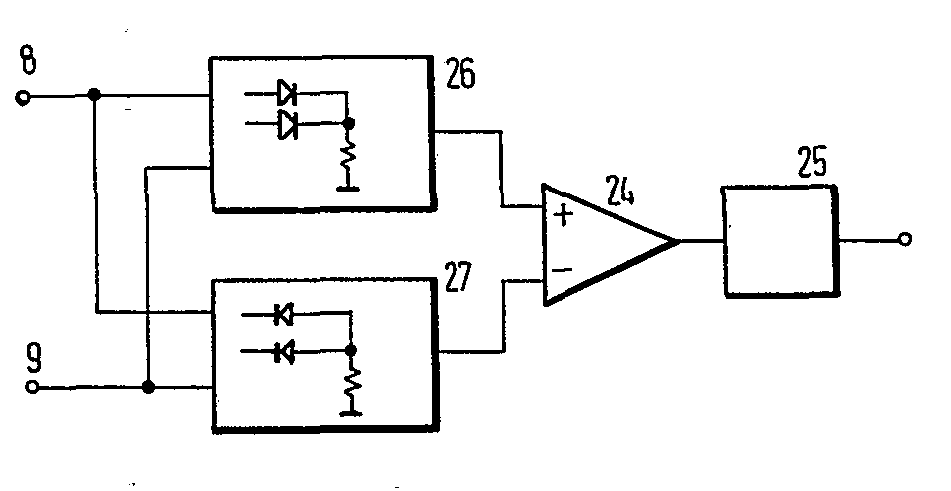
Description
Die Erfindung betrifft ein Verfahren nach der Gattung des Hauptanspruchs. Sowohl bei Flächen- als auch zeilenförmigen optoelektronischen Halbleiter-Sensoren werden Ladungen, welche der jeweiligen Helligkeit einzelner Bildpunkte entsprechen, im Takt von Taktsignalen zu einem Ausgang bzw. zu mehreren Ausgängen transportiert und sind dann als Signal abnehmbar.The invention relates to a method according to the preamble of the main claim. In the case of areal as well as line-shaped optoelectronic semiconductor sensors, charges which correspond to the respective brightness of individual pixels are transported in time with clock signals to one output or to several outputs and are then removable as a signal.
Der Signalverlauf einer Taktperiode ist derart, daß ein jeweils von der Helligkeit abhängiger MaximalWert auf einen von der Helligkeit unabhängigen Minimalwert folgt.The signal curve of a clock period is such that a maximum value dependent on the brightness follows a minimum value independent of the brightness.
Bei häufig verwendeten Halbleiter-Sensoren sind zwei Ausgänge vorgesehen, deren Ausgangssignale um 180 phasenverschoben sind. Da die Ausgangssignale der Sensoren sehr klein sind, sind entsprechende Ver- starker vorgesehen, welche bei einigen Halbleiter- Sensoren bereits in diesen Sensoren integriert sind.In the case of frequently used semiconductor sensors, two outputs are provided, the output signals of which are phase-shifted by 180. Since the output signals of the sensors are very small, corresponding stronger provided, which are already integrated in some semiconductor sensors in these sensors.
In den Verstärkern entsteht nun ein Rauschsignal, welches sich additiv dem Nutzsignal überlagert.A noise signal now arises in the amplifiers, which is superimposed on the useful signal.
Aufgabe der vorliegenden Erfindung ist es, dieses Rauschen zu unterdrücken.The object of the present invention is to suppress this noise.
Das erfindungsgemäße Verfahren mit den kennzeichnenden Merkmalen des Hauptanspruchs hat den Vorteil, daß dieser, im wesentlichen niederfrequente Rauschanteil weitgehend unterdrückt wird.The method according to the invention with the characterizing features of the main claim has the advantage that this essentially low-frequency noise component is largely suppressed.
Durch die in den Unteransprüchen aufgeführten Maßnahmen sowie durch die erfindungsgemäße Anordnungen zur Durchführung des Verfahrens sind vorteilhafte Weiterbildungen und Verbesserungen des im Hauptanspruch angegebenen Verfahrens möglich.Advantageous further developments and improvements of the method specified in the main claim are possible through the measures listed in the subclaims and through the arrangements according to the invention for performing the method.
Ausführungsbeispiele der Erfindung sind in der Zeichnung anhand mehrerer Figuren dargestellt und in der nachfolgenden Beschreibung näher erläutert.Exemplary embodiments of the invention are shown in the drawing using several figures and are explained in more detail in the following description.
- Fig. 1 zeigt schematisch einen Halbleiter-Sensor,1 schematically shows a semiconductor sensor,
- Fig. 2 das Signal- und Rauschspektrum des Ausgangssignals eines Halbleiter-Sensors,2 shows the signal and noise spectrum of the output signal of a semiconductor sensor,
- Fig. 3 ein erstes Ausführungsbeispiel,3 shows a first exemplary embodiment,
- Fig. 4 ein zweites Ausführungsbeispiel,4 shows a second embodiment,
- Fig. 5 ein drittes Ausführungsbeispiel,5 shows a third embodiment,
- Fig. 6 ein viertes Ausführungsbeispiel undFig. 6 shows a fourth embodiment and
- Fig. 7 ein fünftes Ausführungsbeispiel.Fig. 7 shows a fifth embodiment.
Bei dem Halbleiter-Sensor nach Fig. 1 stellt 1 den eigentlichen Bildbereich dar, während die Schieberegister 2 und 3 im Takt von bei 4 und 5 zugeführten Taktimpulsen die Ladungen aus dem Bildbereich zu den Ausgängen transportieren. An den Ausgängen der Schieberegister 2, 3 ist je ein Verstärker 6, 7 angeordnet, an dessen Ausgängen 8 und 9 die Signale, deren zeitlicher Verlauf schematisch dargestellt ist, abnehmbar sind.1 represents the 1 represents the actual image area, while
Die Ausgangssignale weisen das in Fig. 2 dargestellte Spektrum auf, welches bei einer Abtastfrequenz von 10 MHz ein Basisband bis etwa 5-MHz umfaßt. Zur Gewinnung von Videosignalen wird dieses Basisband üblicherweise durch einen Tiefpaß abgetrennt, so daß ein Videosignal entsprechend der mit 10 bezeichneten Spektralverteilung auftritt. Wie eingangs erwähnt, ist diesem Signal Rauschen überlagert, dessen Spektralverteilung etwa der Kurve 11 entspricht.The output signals have the spectrum shown in FIG. 2, which comprises a baseband up to approximately 5 MHz at a sampling frequency of 10 MHz. To obtain video signals, this baseband is usually separated by a low-pass filter, so that a video signal corresponding to the spectral distribution denoted by 10 occurs. As mentioned at the beginning, noise is superimposed on this signal, the spectral distribution of which roughly corresponds to curve 11.
Das Spektrum der bei 8 und 9 (Fig. 1) anstehenden Signale umfaßt ferner einen Träger bei 10 MHz sowie dessen Seitenbänder von t 5 MHz.The spectrum of the signals present at 8 and 9 (FIG. 1) also includes a carrier at 10 MHz and its sidebands of
In Fig. 3a ist ein erstes Ausführungsbeispiel dargestellt, während Fig. 3b eines der Ausgangssignale des Halbleiter-Sensors darstellt, welches mit additivem Rauschen überlagert ist. Da das Rauschen additv überlagert ist, macht es sich bei den Maximal- und Minimal-Werten gleichermaßen bemerkbar. Die Signale werden nun von den Ausgängen 8, 9 (Fig. 1) über ImpedanzWandler 12, 13 Klemmschaltungen 14, 15, 16, 17 zugeführt. Die Schalter 16 und 17 werden jeweils geschlossen, wenn das entsprechende Signal seinen Minimal-Wert aufweist. An die Klemmschaltungen schließen sich Verstärker 18 und 19 an, deren Ausgänge zur Zusammenfassung beider Signale an eine Addierschaltung 20, welche auch als nichtadditive Mischschaltung ausgebildet sein kann, angeschlossen sind. Mit Hilfe eines Tiefpasses werden die trägerfrequenten Anteile entfernt.FIG. 3a shows a first exemplary embodiment, while FIG. 3b shows one of the output signals of the semiconductor sensor, which is superimposed with additive noise. Since the noise is additionally superimposed, it is equally noticeable in the maximum and minimum values. The signals are now fed from the
Bei dem Ausführungsbeispiel nach Fig. 4 werden die Minimal- und Maximal-Werte durch Schwellwertschaltungen voneinander getrennt. Die Ausgangssignale der Schwellwertschaltungen 22 und 23 werden den Eingängen einer Subtrahierschaltung 24 zugeführt. Dadurch wird erreicht, daß lediglich die Differenz zwischen den Maximal- und Minimal-Werten ermittelt wird und über den Tiefpaß 25 als Videosignal zur Verfügung steht. Bei der Anordnung nach Fig. 5 erfolgt die Trennung der Minimal- und Maximal-Werte durch nichtadditive Mischschaltungen 26 und 27, welche im wesentlichen aus jeweils zwei Transistoren bestehen, welche über ihre Emitter mit einem gemeinsamen Arbeitswiderstand verbunden sind.In the exemplary embodiment according to FIG. 4, the minimum and maximum values are separated from one another by threshold value circuits. The output signals of the
Da sich das Rauschen, wie aus Fig. 2 ersichtlich ist, fast ausschließlich im Basisband bemerkbar macht, kann eine Unterdrückung des Rauschens auch dadurch erfolgen, daß das Trägerband zur Gewinnung des Videosignals ausgenutzt wird.Bei der Anordnung nach Fig. 6 werden hierzu die Ausgangssignale über je einen Bandpaß 28, 29 geleitet, dessen Durchlaßbereich von 5 MHz bis 15 MHz reicht. Beide trägerfrequenten Signale werden einem Hüllkurven-Demodulator 30 zugeführt, dessen Ausgangssignal über einen Verstärker 31 und einen Tiefpaß 32 dem Ausgang 33 der Anordnung nach Fig. 6 zugeleitet ist.Since the noise, as can be seen from FIG. 2, is almost exclusively noticeable in the baseband, the noise can also be suppressed by using the carrier band to obtain the video signal. In the arrangement according to FIG. 6, the output signals are used for this routed via a
Da durch die Taktung des Halbleiter-Sensors die Trägerfrequenz ohnehin zur Verfügung steht, kann gemäß Fig. 7 ein Synchron-Demodulator in einfacher Weise dazu verwendet werden, das Trägerband in das Basisband umzusetzen. Hierzu sind für jeden der Ausgänge des Halbleiter-Sensors Synchron-Demodulatoren 34, 35 vorgesehen. Diesen wird bei 36 und 37 jeweils ein Taktsignal zugeführt. Die Ausgänge der Synchron-Demodulatoren sind mit den Eingängen einer Addierschaltung 38 verbunden, an deren Ausgang ein Tiefpaß 39 angeschlossen ist.Since the carrier frequency is available anyway due to the timing of the semiconductor sensor, a synchronous demodulator can be used in a simple manner according to FIG. 7 to convert the carrier band into the baseband. This is done for each of the outputs of the semiconductor sensor
Fig. 8 zeigt in detaillierter Darstellung ein Ausführungsbeispiel gem. Fig.5, wobei Fig. 8a die Schaltung selbst und Fig. 8b Spannungs-Zeitdiagramme der bei der Schaltungsanordnung auftretenden Signale darstellt.Fig. 8 shows a detailed representation of an embodiment. Fig. 5, Fig. 8a shows the circuit itself and Fig. 8b voltage-time diagrams of the signals occurring in the circuit arrangement.
Der Schaltung nach Fig. 8a werden an den Punkten 8 und 9 jeweils die Ausgangssignale des Sensors zugeführt. Die entsprechenden Ausgangsschaltungen des Sensors (s. Fig. 1) sind in Fig. 8a lediglich schematisch als Generatoren 51 und 52 dargestellt. Die Form der bei 8 und 9 der Schaltungsanordnung nach Fig. 8a zugeführten Signale ist in Fig. 8b in den Zeilen a1 und a2 dargestellt.The circuit according to FIG. 8a is supplied with the output signals of the sensor at
Da die Schieberegister 2 und 3 (Fig. 1) abwechselnd getaktet werden, ergibt sich ein entsprechend phasenverschobenes Auslesen der Signale. Die sich ergebende Impulsform ist in Fig. 8b schematisch als dreieckförmige Spannung angegeben, wobei die jeweils nach oben gezeichnete Amplitude in demjenigen Impulsintervall abgegeben wird, in welchem keine Information aus dem Sensor ausgelesen wird, während die in Fig. 8b nach unten gezeichnete Amplitude der jeweils ausgelesenen Information entspricht. In Fig. 8b, Zeile a1, wird angenommen, daß das ausgelesene Signal der maximalen Belichtung (ws = weiß) entspricht, während der Pegel für den unbelichteten Sensor lediglich gestrichelt dargestellt ist (sw = schwarz). Bei dem in Fig. 8b, Zeile a2, dargestellten Signal wird von einem unbelichteten Sensor ausgegangen, der Pegel für Maximalbelichtung (ws) ist gestrichelt dargestellt.Since the shift registers 2 and 3 (FIG. 1) are clocked alternately, the signals are read out correspondingly out of phase. The resulting pulse shape is shown schematically in FIG. 8b as a triangular voltage, the amplitude drawn upwards being given in the pulse interval in which no information is read out from the sensor, while the amplitude drawn downwards in FIG. 8b is given in each case read information corresponds. In Fig. 8b, line a1, it is assumed that the read signal corresponds to the maximum exposure (ws = white), while the level for the unexposed sensor is only shown in dashed lines (sw = black). The signal shown in FIG. 8b, line a2, is based on an unexposed sensor, the level for maximum exposure (ws) is shown in dashed lines.
Beiden Signalen ist nun ein Rauschen überlagert, welches im wesentlichen durch die Verstärker 6 und 7 (Fig. 1) verursacht ist. Da dieses Rauschen additiv überlagert ist, ändern sich die Minimal- und Maximal- werte der in Zeilen a1 und a2 dargestellten Signale gleichsinnig. Bei der gewählten Darstellung wurde angenommen, daß die Rauschspannung in den beiden Kanälen verschiedene Frequenzen aufweist.Noise is superimposed on both signals, which is essentially caused by
Beide Signale werden nun je einer Impedanzwandlerstufe, jeweils bestehend aus einem Transistor 53, 54,einem Basiswiderstand 55,56 und einem Emitterwiderstand 57, 58. Die Kollektoren der Transistoren 53 und 54 sind an den positiven Pol 59 der Betriebsspannungsquelle von beispielsweise + 15V angeschlossen, während die Arbeitswiderstände 57 und 58 mit dem Pol 60 einer negativen Betriebsspannungsquelle von beispielsweise 12V verbunden sind. Vom Ausgang des Impedanzwandlers gelangen die Signale zu je einer Schwarzsteuerschaltung, welche jeweils aus einem Kondensator 61,62 einem Transistor 63,64 sowie einem Widerstand 65,66 besteht. Diese Schwarzsteuerschaltung legt den Arbeitspunkt der nachfolgenden Schaltungen fest. Zur Gewährleistung einer genügend großen Zeitkonstante der Schwarzsteureschaltungen sind an diese weitere Impedanzwandler, bestehend aus den Feldeffekttransistoren 67 und 68 angeschlossen, deren Arbeitswiderstände die Widerstände 69 und 70 sind und welche mit den Basen der Transistoren 71 und 72 verbunden sind, die wiederum untereinander emittergekoppelt sind und einen gemeinsamen Emitterwiderstand 73 aufweisen.Both signals are now each an impedance converter stage, each consisting of a
Die Transistoren 71 und 72 wirken als sogenannte NAM-Schaltung (nicht additive Mischung). Von denjenigen Spannungen, welche den Basen der Transistoren 71 und 72 zugeführt werden, wird diejenige zum Schaltungspunkt 74 weitergeleitet, welche einen negativeren Momentanwert aufweist.The
Wegen der zeitlich versetzten Ansteuerung der beiden Sensorausgänge 8 und 9 wird abwechselnd von beiden Sensoren der negative Spitzenwert des Ausgangssignals zum Schaltungspunkt 74 geleitet. Dieser negative Spitzenwert verkörpert - wie im Zusammenhang mit Fig. 8b erläutert - das Nutzsignal, welchem die Rauschspannung überlagert ist. In Fig. 8a wurde deshalb die Spannung am Schaltungspunkt 74 mit US+N bezeichnet, wobei S für signal und N für noise steht. Eine ähnliche NAM-Schaltung ist mit Hilfe der Transistoren 73'und 74'und mit Hilfe des Widerstandes 75 aufgebaut, wobei die Transistoren 73'und 74'vom entgegengesetzten Leitfähigkeitstyp wie die Transistoren 71 und 72 sind. Daraus ergibt sich, daß die zweite NAM-Schaltung die positiven Spitzen des in Zeile b der Fig. 8b gezeigten Signals weiterleitet. Diese enthalten lediglich die Rauschspannung und sind daher mit UN gekennzeichnet.Because the actuation of the two
Erfindungsgemäß sollen nun die Ausgangsspannungen der NAM-Schaltungen voneinander subtrahiert werden. Dieses erfolgt in einem Operationsverstärker 76, welcher mit Hilfe des Widerstandes 77 gegengekoppelt ist. Der invertierende Eingang des Operationsverstärkers 76 ist mit der Spannung US+N beaufschlagt, wozu diese über einen Impedanzwandler geleitet wird. Der Impedanzwandler besteht aus dem Transistor 78, dem Basiswiderstand 79 und dem Arbeitswiderstand 80. Ferner ist ein einstellbarer Längswiderstand 81, mit dessen Hilfe die Verstärkung des Operationsverstärkers 76 eingestellt werden kann, und ein Widerstand 82 zur Zuführung einer Vorspannung vorgesehen. Zur Entkoppelung des Gleichspannungspotentials zwischen der NAM-Schaltung und dem Impedanzwandler dient ein Kondensator 83.According to the invention, the output voltages of the NAM circuits are now to be subtracted from one another. This takes place in an
Die Spannung UN wird ebenfalls über einen Kondensator 84 und einen Impedanzwandler dem nichtinvertierenden Eingang des Operationsverstärkers 76 zugeführt. Der Impedanzwandler besteht aus dem Transistor 85, dem Basiswiderstand 86 und dem Arbeitswiderstand 87.The voltage U N is also supplied to the non-inverting input of the
Der Ausgang des Operationsverstärkers 76 ist über einen Widerstand 88, einen Tiefpaß 89 mit einer Grenzfrequenz von etwa 5,5MHz mit dem Ausgang 90 der Schaltungsanordnung verbunden. Der Tiefpaß 89 dient dazu, die Abtastfrequenz sowie deren Seitenbänder aus dem Signalgemisch herauszufiltern, so daß lediglich das Videofrequenzband erhalten bleibt.The output of the
In Fig. 8b ist ferner in Zeile c1 die Überlagerung der beiden Rauschanteile dargestellt, während in Zeile c2 die Modulation bzw. das Nutzsignal zusammen mit den beiden Rauschanteilen gezeigt ist. Die Diagramme c1 und c2 stellen also die Signale UN und US+N dar. Die Subtraktion beider Signale ergibt das in Zeile b dargestellte Ergebnis.In FIG. 8b line c1 also shows the superposition of the two noise components, while line c2 shows the modulation or the useful signal together with the two noise components. The diagrams c1 and c2 thus represent the signals U N and U S + N. The subtraction of both signals gives the result shown in line b.
Claims (11)
Applications Claiming Priority (2)
| Application Number | Priority Date | Filing Date | Title |
|---|---|---|---|
| DE19803049043 DE3049043A1 (en) | 1980-12-24 | 1980-12-24 | METHOD AND ARRANGEMENT FOR SUPPRESSING LOW-FREQUENCY NOISE ON OUTPUT SIGNALS FROM SEMICONDUCTOR SENSORS |
| DE3049043 | 1980-12-24 |
Publications (3)
| Publication Number | Publication Date |
|---|---|
| EP0054738A2 true EP0054738A2 (en) | 1982-06-30 |
| EP0054738A3 EP0054738A3 (en) | 1985-01-30 |
| EP0054738B1 EP0054738B1 (en) | 1988-03-09 |
Family
ID=6120290
Family Applications (1)
| Application Number | Title | Priority Date | Filing Date |
|---|---|---|---|
| EP81109458A Expired EP0054738B1 (en) | 1980-12-24 | 1981-10-31 | Method and apparatus for low-frequency noise suppression in the output signals of semiconducteur sensors |
Country Status (4)
| Country | Link |
|---|---|
| US (1) | US4488052A (en) |
| EP (1) | EP0054738B1 (en) |
| JP (1) | JPS57131180A (en) |
| DE (2) | DE3049043A1 (en) |
Cited By (2)
| Publication number | Priority date | Publication date | Assignee | Title |
|---|---|---|---|---|
| EP0213684A1 (en) * | 1985-09-04 | 1987-03-11 | Koninklijke Philips Electronics N.V. | Camera for recording television, photographic or cinematographic images |
| EP0161752A3 (en) * | 1984-04-13 | 1988-06-22 | Kabushiki Kaisha Toshiba | Image signal reproduction circuit for swing image sensor |
Families Citing this family (5)
| Publication number | Priority date | Publication date | Assignee | Title |
|---|---|---|---|---|
| JPS60111579A (en) * | 1983-11-21 | 1985-06-18 | Nec Corp | Signal charge detection circuit of charge transfer device |
| US5926217A (en) * | 1993-07-27 | 1999-07-20 | Drs Technologies, Inc. | Focal plane array integrated circuit with individual pixel signal processing |
| US5703353A (en) * | 1996-01-25 | 1997-12-30 | Hewlett-Packard Company | Offset removal and spatial frequency band filtering circuitry for photoreceiver signals |
| US6180936B1 (en) | 1996-09-03 | 2001-01-30 | Siemens Aktiengesellschaft | Photoreceptor arrangement for receiving light beams having coupling elements |
| TWI477747B (en) * | 2012-05-08 | 2015-03-21 | Egalax Empia Technology Inc | Detecting method and device for suppressing interference of low frequency noise |
Family Cites Families (9)
| Publication number | Priority date | Publication date | Assignee | Title |
|---|---|---|---|---|
| FR1381103A (en) * | 1963-02-01 | 1964-12-04 | Marconi Instruments Ltd | Improvements to television cameras and the like |
| US3830972A (en) * | 1972-11-13 | 1974-08-20 | Ibm | Sensitivity compensation for a self scanned photodiode array |
| JPS524113A (en) * | 1975-06-28 | 1977-01-13 | Nippon Hoso Kyokai <Nhk> | Solid pickup equipment |
| US4009334A (en) * | 1976-03-17 | 1977-02-22 | Eastman Kodak Company | Video noise reduction circuit |
| NL7613357A (en) * | 1976-12-01 | 1978-06-05 | Philips Nv | TELEVISION ROOM EQUIPPED WITH A TELEVISION TUBE AND A COMPENSATION CIRCUIT FOR LOW FREQUENCY SIGNAL INTERFERENCE, IN PARTICULAR MICROPHONY. |
| JPS5822900B2 (en) * | 1978-09-25 | 1983-05-12 | 株式会社日立製作所 | solid-state imaging device |
| JPS56116374A (en) * | 1980-02-20 | 1981-09-12 | Sony Corp | Charge detection circuit |
| US4317134A (en) * | 1980-05-12 | 1982-02-23 | Eastman Kodak Company | Method and apparatus for pattern noise correction |
| US4412190A (en) * | 1981-11-05 | 1983-10-25 | Rca Corporation | Apparatus for processing CCD output signals |
-
1980
- 1980-12-24 DE DE19803049043 patent/DE3049043A1/en not_active Ceased
-
1981
- 1981-10-31 EP EP81109458A patent/EP0054738B1/en not_active Expired
- 1981-10-31 DE DE8181109458T patent/DE3176683D1/en not_active Expired
- 1981-12-08 US US06/328,475 patent/US4488052A/en not_active Expired - Fee Related
- 1981-12-24 JP JP56208216A patent/JPS57131180A/en active Granted
Cited By (2)
| Publication number | Priority date | Publication date | Assignee | Title |
|---|---|---|---|---|
| EP0161752A3 (en) * | 1984-04-13 | 1988-06-22 | Kabushiki Kaisha Toshiba | Image signal reproduction circuit for swing image sensor |
| EP0213684A1 (en) * | 1985-09-04 | 1987-03-11 | Koninklijke Philips Electronics N.V. | Camera for recording television, photographic or cinematographic images |
Also Published As
| Publication number | Publication date |
|---|---|
| US4488052A (en) | 1984-12-11 |
| JPS57131180A (en) | 1982-08-13 |
| EP0054738B1 (en) | 1988-03-09 |
| DE3049043A1 (en) | 1982-07-15 |
| DE3176683D1 (en) | 1988-04-14 |
| JPH0224069B2 (en) | 1990-05-28 |
| EP0054738A3 (en) | 1985-01-30 |
Similar Documents
| Publication | Publication Date | Title |
|---|---|---|
| DE2713953C3 (en) | Harmonic generator for generating the third harmonic | |
| DE2854236C2 (en) | Color television receiver with at least partially digital signal processing and with at least one integrated circuit for the luminance signal and the chrominance signals | |
| DE2053513B2 (en) | Method and arrangement for avoiding the loss of resolution in the vertical direction of a color television picture | |
| DE2524072C2 (en) | Power amplifier for signals modulated in the pulse width | |
| DE3036905A1 (en) | SIGNAL PROCESSING CIRCUIT FOR SOLID-CAMERA | |
| DE2712024A1 (en) | CIRCUIT ARRANGEMENT FOR REGENERATING SYNCHRONOUS SIGNALS | |
| DE2317739C3 (en) | ||
| DE3631131A1 (en) | CIRCUIT ARRANGEMENT FOR OBTAINING USER SIGNALS FROM A SOLID-STATE IMAGE CONVERTER | |
| EP0054738B1 (en) | Method and apparatus for low-frequency noise suppression in the output signals of semiconducteur sensors | |
| DE2833216C2 (en) | Circuit arrangement for clamping the blanking level and the control voltage for the picture tube of a television technical device | |
| DE3002738C2 (en) | Arrangement for separating television sync signals | |
| DE2946358C2 (en) | ||
| DE3141257A1 (en) | COLOR SIGNAL PROCESSING CIRCUIT | |
| DD155573A5 (en) | MODULATOR CIRCUIT FOR AMPLITUDE MODULATION OF AN IMAGE SIGNAL TO A SUPPLY SIGNAL | |
| DE3042059C2 (en) | Television receiver for receiving an image carrier which is amplitude-modulated with a video signal and an audio carrier which is frequency-modulated with a sound signal | |
| DE3610190C2 (en) | ||
| DE2836144C3 (en) | Video signal processing circuit | |
| DE2606486A1 (en) | SIGNAL DEMODULATION CIRCUIT | |
| DE3443068A1 (en) | DEVICE FOR CONTOUR CORRECTION IN THE VERTICAL DIRECTION OF AN IMAGE | |
| DE2821773A1 (en) | SYNCHRONOUS DETECTOR | |
| DE2223908C3 (en) | Circuit for eliminating the sync pulses S in a BAS video signal | |
| DE2711586C3 (en) | Circuit for generating special effects on color television pictures, in particular for titling | |
| DE2832269C2 (en) | Monolithic integrated circuit for the horizontal deflection of television sets and their operating circuit | |
| DE2022291A1 (en) | Amplifier circuit, especially for a color television receiver | |
| DE2044352C3 (en) | Circuit for blanking color television signals |
Legal Events
| Date | Code | Title | Description |
|---|---|---|---|
| PUAI | Public reference made under article 153(3) epc to a published international application that has entered the european phase |
Free format text: ORIGINAL CODE: 0009012 |
|
| 17P | Request for examination filed |
Effective date: 19811031 |
|
| AK | Designated contracting states |
Designated state(s): DE FR GB |
|
| PUAL | Search report despatched |
Free format text: ORIGINAL CODE: 0009013 |
|
| AK | Designated contracting states |
Designated state(s): DE FR GB |
|
| 17Q | First examination report despatched |
Effective date: 19860619 |
|
| RAP1 | Party data changed (applicant data changed or rights of an application transferred) |
Owner name: ROBERT BOSCH GMBH |
|
| GRAA | (expected) grant |
Free format text: ORIGINAL CODE: 0009210 |
|
| AK | Designated contracting states |
Kind code of ref document: B1 Designated state(s): DE FR GB |
|
| REF | Corresponds to: |
Ref document number: 3176683 Country of ref document: DE Date of ref document: 19880414 |
|
| ET | Fr: translation filed | ||
| GBT | Gb: translation of ep patent filed (gb section 77(6)(a)/1977) | ||
| PLBE | No opposition filed within time limit |
Free format text: ORIGINAL CODE: 0009261 |
|
| STAA | Information on the status of an ep patent application or granted ep patent |
Free format text: STATUS: NO OPPOSITION FILED WITHIN TIME LIMIT |
|
| 26N | No opposition filed | ||
| REG | Reference to a national code |
Ref country code: GB Ref legal event code: 746 |
|
| PGFP | Annual fee paid to national office [announced via postgrant information from national office to epo] |
Ref country code: FR Payment date: 19911030 Year of fee payment: 11 |
|
| PG25 | Lapsed in a contracting state [announced via postgrant information from national office to epo] |
Ref country code: FR Effective date: 19930630 |
|
| REG | Reference to a national code |
Ref country code: FR Ref legal event code: ST |
|
| PGFP | Annual fee paid to national office [announced via postgrant information from national office to epo] |
Ref country code: GB Payment date: 19930929 Year of fee payment: 13 |
|
| PGFP | Annual fee paid to national office [announced via postgrant information from national office to epo] |
Ref country code: DE Payment date: 19931223 Year of fee payment: 13 |
|
| PG25 | Lapsed in a contracting state [announced via postgrant information from national office to epo] |
Ref country code: GB Effective date: 19941031 |
|
| GBPC | Gb: european patent ceased through non-payment of renewal fee |
Effective date: 19941031 |
|
| PG25 | Lapsed in a contracting state [announced via postgrant information from national office to epo] |
Ref country code: DE Effective date: 19950701 |