EP0054943A1 - Leistungsverstärker, bei dem die Leistung von einer geschalteten Speisespannungsquelle an eine Last geliefert wird - Google Patents
Leistungsverstärker, bei dem die Leistung von einer geschalteten Speisespannungsquelle an eine Last geliefert wird Download PDFInfo
- Publication number
- EP0054943A1 EP0054943A1 EP81110608A EP81110608A EP0054943A1 EP 0054943 A1 EP0054943 A1 EP 0054943A1 EP 81110608 A EP81110608 A EP 81110608A EP 81110608 A EP81110608 A EP 81110608A EP 0054943 A1 EP0054943 A1 EP 0054943A1
- Authority
- EP
- European Patent Office
- Prior art keywords
- voltage
- circuit
- output
- input signal
- switching element
- Prior art date
- Legal status (The legal status is an assumption and is not a legal conclusion. Google has not performed a legal analysis and makes no representation as to the accuracy of the status listed.)
- Granted
Links
- 238000009499 grossing Methods 0.000 claims abstract description 69
- 230000000295 complement effect Effects 0.000 claims description 8
- 230000004069 differentiation Effects 0.000 claims description 5
- 230000008878 coupling Effects 0.000 claims 1
- 238000010168 coupling process Methods 0.000 claims 1
- 238000005859 coupling reaction Methods 0.000 claims 1
- 238000010586 diagram Methods 0.000 description 7
- 230000000694 effects Effects 0.000 description 5
- 239000003990 capacitor Substances 0.000 description 4
- 230000007423 decrease Effects 0.000 description 2
- 230000003111 delayed effect Effects 0.000 description 2
- 230000003321 amplification Effects 0.000 description 1
- 239000002131 composite material Substances 0.000 description 1
- 230000002596 correlated effect Effects 0.000 description 1
- 230000002708 enhancing effect Effects 0.000 description 1
- 230000005669 field effect Effects 0.000 description 1
- 238000003199 nucleic acid amplification method Methods 0.000 description 1
- 230000000630 rising effect Effects 0.000 description 1
Images


Classifications
-
- H—ELECTRICITY
- H03—ELECTRONIC CIRCUITRY
- H03F—AMPLIFIERS
- H03F1/00—Details of amplifiers with only discharge tubes, only semiconductor devices or only unspecified devices as amplifying elements
- H03F1/02—Modifications of amplifiers to raise the efficiency, e.g. gliding Class A stages, use of an auxiliary oscillation
- H03F1/0205—Modifications of amplifiers to raise the efficiency, e.g. gliding Class A stages, use of an auxiliary oscillation in transistor amplifiers
- H03F1/0211—Modifications of amplifiers to raise the efficiency, e.g. gliding Class A stages, use of an auxiliary oscillation in transistor amplifiers with control of the supply voltage or current
- H03F1/0216—Continuous control
- H03F1/0222—Continuous control by using a signal derived from the input signal
- H03F1/0227—Continuous control by using a signal derived from the input signal using supply converters
-
- H—ELECTRICITY
- H03—ELECTRONIC CIRCUITRY
- H03F—AMPLIFIERS
- H03F3/00—Amplifiers with only discharge tubes or only semiconductor devices as amplifying elements
- H03F3/50—Amplifiers in which input is applied to, or output is derived from, an impedance common to input and output circuits of the amplifying element, e.g. cathode follower
-
- H—ELECTRICITY
- H03—ELECTRONIC CIRCUITRY
- H03F—AMPLIFIERS
- H03F2200/00—Indexing scheme relating to amplifiers
- H03F2200/511—Many discrete supply voltages or currents or voltage levels can be chosen by a control signal in an IC-block amplifier circuit
Definitions
- the present invention relates to a power amplifier suitable for an audio amplifier.
- Class A or Class B SEPP signal-ended push-pull power amplifiers are generally used.
- Class A SEPP power amplifier generates less distortion, because output transistors thereof require a relatively large idling current the amount of heat generated increases as the output power decreases. At the maximum output power level, the power dissipation is generated as much as the output signal power.
- Class B SEPP power amplifier uses no idling current, both the cross-over distortion and the switching distortion take place, while the efficiency thereof is much higher than that of the Class A SEPP power amplifier. Still, the efficiency of the Class B SEPP power amplifier at the maximum output power level reaches at most 78 %, and at smaller output power levels the efficiency thereof more decreases.
- a power amplifier which is much higher in efficiency than the Class B power amplifier.
- This power amplifier is provided with an emitter follower transistor having its base connected to receive an audio input signal.
- the collector voltage and the emitter voltage (terminal voltage of a load, that is, an output voltage) of the emitter follower transistor are compared by a voltage comparator having a hysteresis characteristic.
- This voltage comparator controls a switching element which supplies the collector of the emitter follower transistor with a power supply voltage. Between the switching element and the emitter follower transistor a smoothing circuit is connected.
- This'power amplifier achieves a higher efficiency than the Class B power amplifier by making the collector voltage of the emitter follower transistor follow the waveform of the input signal. It is, however, indispensable for this power amplifier to have an emitter follower transistor. If the high frequency characteristic of the emitter follower transistor is poor, the waveform of the emitter voltage or the output voltage of the emitter follower transistor is delayed from the waveform of input signal voltage and the waveform of the collector_voltage is further delayed, thereby causing generation of distortion.
- Another object of the present invention is to provide a power amplifier which is arranged to vary an output voltage of an output amplifying element and a power supply voltage thereof in accordance with an input signal voltage and to lower the delay of the variation in the power supply voltage of the output power amplifying element from the variation in the output voltage thereof.
- the objects of the present invention can be achieved by providing, in an power amplifier in which a DC power supply is connected to a load via a switching element and a smoothing circuit in order to vary the load terminal voltage in accordance with an input signal voltage, a voltage detecting circuit which compares a feedback voltage proportional to the output voltage of the smoothing circuit with the input signal voltage to switch the switching element.
- This voltage detecting circuit has two different switching levels of the feedback voltage relative to the input signal voltage for switching the switching element from ON to OFF and from OFF to ON. Namely, the voltage detecting circuit has a hysteresis characteristic.
- the input signal voltage to be amplified is compared with the output voltage of the smoothing circuit, thereby making it possible to minimize the delay of the variation in output voltage of the smoothing circuit.
- an output amplifying element such as emitter follower transistor may be connected.
- the input of the amplifying element is supplied with the input signal voltage.
- an output voltage from which ripple components are removed can be applied to the load.
- the power amplifier of the present invention may be applied to Class B SEPP and Class A SEPP amplifiers.
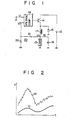
- Fig. 1 shows a basic_circuit arrangement of the present invention, in which reference numeral 11 represents an input terminal to which an input signal Vi is applied, reference numeral 12 a D C power supply, and reference numeral 13 a load such as loudspeaker.
- switching element 14 a transistor, for example, as shown
- DC power supply 12 DC power supply 12
- a smoothing circuit 16 having a.choke coil 17 and a capacitor 18.
- Reference numeral 19 designates a voltage comparator circuit to control switching element 14, of which one input receives input signal Vi applied to input terminal 11, while the other input receives an output voltage Vf of a voltage dividing circuit 20, which comprises resistors 21 and 22, to divide an output voltage Vo of smoothing circuit 16.
- Comparator 20 is arranged to switch switching element 14 from OFF to ON when Vf-Vi exceeds - ⁇ V and from ON to OFF when Vf-Vi exceeds + ⁇ V. Namely, voltage comparator 20 has a hysteresis characteristic.
- the aforementioned switching action of switching element 14 causes the output voltage of the smoothing circuit 16, that is, the output voltage Vo to be supplied to load 13 to vary in accordance with the input signal voltage Vi as shown in Fig. 2.
- lettinq the dividinq factor of voltage dividing circuit 20 be (where R21 and R22 are values of resistors 21 and 22, respectively), the waveform of output.
- voltage Vo is represented by the sum of a waveform having a voltage n times as large as input signal voltage Vi and triangular-waves having a peak-to-peak value of 2nAV (ripple component).
- the ripple component exerts no influence on listner's sense of hearing as the switching frequency (above 100 kHz) of switching element 14 is out of the audible frequency range, but threatens to cause spurious emission.
- the ripple voltage can be lowered by making the values of n and ⁇ V small.
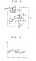
- FIG. 3 there is shown another embodiment of the present invention which comprises an emitter follower transistor 30 connected between smoothing circuit 16 and load 13 as an output amplifying element and having its base connected to receive input signal voltage Vi.
- This circuit aims at reducing the ripple component in the load terminal voltage Vo with the aid of emitter follower transistor 30.
- voltage comparator circuit. 19 of this power amplifier a positive fixed bias voltage is added to input signal voltage Vi, which is then compared with the feedback voltage Vf. Accordingly, as shown in Fig. 4, the collector voltage Vc of transistor 30 contains ripple component, while the output voltage Vo exhibits a waveform which contains no ripple component and varies in accordance with input signal voltage Vi.
- the positive bias voltage is added to input signal voltage Vi the collector voltage of transistor 30 is always higher than the emitter voltage thereof, thereby ensuring the stable operation of transistor 30 and enhancing the ripple removing effect.
- a certain extent of ripple component leak from the collector to the emitter of transistor 30 due to the existence of a capacitance between the collector and base thereof.
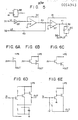
- Fig. 5 shows a practical arrangement of voltage comparator circuit 19, in which reference numeral 31 designates a terminal to be connected-to input terminal 11 and reference numeral 32 a terminal to receive feedback voltage Vf.
- Input signal voltage Vi is applied to an inverting input of an inverting amplifier 34, having its noninverting input grounded via a buffer amplifier 33 having a gain of unity.
- the inverting input of inverting amplifier 34 is connected with a bias voltage source 35 which adds a positive fixed bias voltage to the input signal voltage Vi.
- the feedback voltage Vf and the output voltage of inverting amplifier 34 are coupled to a noninverting input of an operational ampli-' fier 37 having its inverting input grounded.
- the output terminal of operational amplifier 37 is connected both to an output terminal 38 which is connected to the base of switching transistor 14 and via resistor 42 to diodes 39 and 40 which are connected in parallel and opposite polarity.
- the connection point between resistor 42 and diodes 39 and 40 is connected to the noninverting input of operational amplifier 37 via a feedback resistor 41.
- Reference numerals 43 and 44 represent summing resistors.
- the circuit shown in Fig. 1 needs not have bias voltage source 35 in the voltage comparator circuit 19. Further, while in the. power amplifier circuits shown in Figs. 1 and 3 the output voltage of smoothing circuit 16 is fed back to voltage comparator circuit 19 via voltage dividing circuit 20, the output voltage of smoothing circuit 16 may be fed back directly to voltage comparator circuit 19. Then, the feedback ratio can be determined by resistors 41 and 43 of the voltage comparator circuit 19 shown in Fig. 5.
- the total power dissipation is the sum of- the dissipation of switching element 14 and the collector dissipation of transistor 30, but efficiency of approximately 90 % can be achieved by minimizing the voltage difference between Vc and Vo as shown in Fig. 4. Furthermore, as the voltage between the emitter and collector of transistor 30 is kept nearly constant by the bias voltage, the distortion factor due to the- nonlinearity of the transistor can be made small.
- Output amplifying element 30 shown in Fig. 3 may be substituted by a FET (field effect transistor) as shown in Fig. 6A, a composite transistor-as shown in Figs. 6B and 6C, an amplification circuit having a gain less than unity as shown in Fig. ' 6D, or a phase inverting circuit as shown in Fig. 6E. Namely, any circuit or active element having at-least an input terminal IN, an output terminal OUT, and an power supply terminal PS may be used.
- FET field effect transistor
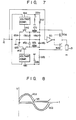
- Fig. 7 shows a Class B SEPP circuit using the arrangement shown in Fig. 3, in which reference numeral 50 represents a driver circuit for output transistors 30a and 30b.
- reference numeral 50 represents a driver circuit for output transistors 30a and 30b.
- the collector voltages Vca and Vcb and output voltage Vo vary as shown in Fig. 8.
- the switching transistor 14b is kept OFF, and the collector voltage Vcb of transistor 30b is kept at a negative constant value by smoothing capacitor 18b when a time constant determined by smoothing capacitor 18b and voltage dividing resistors 21b and 22b is large.
- the collector voltage Vca of transistor 30a varies with the waveshape of an input signal.
- the collector voltage Vca of transistor 30a is kept at a positive constant value by smoothing capacitor 18a as switching transistor 14a is kept OFF, while the collector voltage Vcb of transistor 30b varies with the waveshape of the input signal.
- Fig. 9 shows a Class A SEPP circuit using the arrangement of Fig. 3.
- reference numeral 51 represents a bias circuit for supplying idling current to output transistors 30a and 30b.
- the anode of flywheel diode 15a is connected to negative power source 12b, while the cathode of flywheel diode 15b is connected to positive power source 12a.
- the collector voltage Vca of transistor 30a follows up the negative output voltage as shown in Fig. 10 without being clamped by diode 15a during a negative half cycle of output voltage Vo.
- the output voltage of the smoothing circuit is compared with the input signal voltage, 'so that a delay circuit which compensates the delay of variation in output voltage of the smoothing circuit from the variation in input signal voltage needs not be placed at the input side of output transistor (or transistors).
- a delay circuit which compensates the delay of variation in output voltage of the smoothing circuit from the variation in input signal voltage needs not be placed at the input side of output transistor (or transistors).
- the delay of variation in collector voltage of the output transistor from the variation in emitter output voltage thereof in a high frequency range can be compensated by providing a delay circuit.
- Fig. 11 shows an amplifier circuit arranged to eliminate the waveform distortion due to the application of an input signal voltage having a high slew rate.
- a second switching element 55 is -connected between power source 12 and . collector of output transistor 30 which is controlled by a detecting circuit 56 to detect the rise of input signal voltage Vi.
- the detecting circuit 56 can be arranged, for example, as shown in Fig. 12. Namely, the input signal voltage Vi is differentiated by a differentiation circuit 60 and the resulting output voltage is compared with a reference voltage Vr by a voltage comparator 61. The output voltage of voltage comparator 61 goes low when the output voltage of differentiation circuit'60 exceeds the reference voltage Vr and drives a retrig- gerable monostable multivibrator 62. As a. result, a negative-going output pulse which causes second switching element 55 to be enabled for a certain period is generated by multivibrator 62.
- the amplifier circuit shown in Fig. 11 is arranged such that, when input signal voltage Vi varies at a rate exceeding the rising rate of the ripple triangular wave, the second switching element 55 is turned ON during a fixed period of time to supply the collector of transistor 30 with the power supply voltage. Accordingly, as shown in Fig. 13, even when input signal voltage Vi varies abruptly the output voltage Vo can vary in accordance with the input signal voltage Vi since the collector voltage Vc of transistor 30 is kept at the power supply voltage Vd.
- the ripple component appearing in output voltage Vo is reduced to a considerable extent due to transistor 30.
- the leakage of ripple component from collector to emitter of transistor 30 is due to the collector-base capacitance of transistor 30 and the extent of leakage increases as the switching frequency of switching element 14 becomes higher. To widen an effective range of the frequency characteristic of power amplifier it is necessary to make the switching frequency high.
- Fig. 14 shows a power amplifier arranged to enhance the ripple removing effect.
- another transistor 65 is connected between smoothing circuit 16 and transistor 30.
- diodes 66 are connected between the base of transistor 65 and the base of transistor 30.
- the ripple component which is to be leaked from smoothing circuit 16 to the emitter of transistor 30 is removed first by transistor 65 and next by transistor 30. Accordingly, it will be understood that the power amplifier as shown in Fig. 14 has more a-ripple removing effect than the circuit of Fig. 3. To further enhance the ripple removing effect the number_of transistors may be increased. It is obvious that the circuit arrangement of Fig. 14 may be used to constitute a Class B SEPP circuit and a Class A SEPP circuit.
- the power amplifier of the present invention may be applied to a multi-channel power amplifier.
- Fig. 15 shows a stereo (two channels) single-ended power amplifier,. in which the same reference numerals are used to designate the same parts as those of Fig. 3.
- Output transistors 30R and 30L for right and left channels have their collectors connected in common to the output of smoothing circuit 16, and their emitters respectively grounded via loads 13R and 13L such as loudspeakers.
- the bases of output transistors 30R and 30L are connected to right and left input terminals 11R and 11L, respectively.
- Right and left input terminals 11R and 11L are connected to a voltage detecting circuit 70 which detects one of the right and left channel input signals whose voltage is closer to the voltage of DC power source 12 and couples to voltage comparator circuit 19 the detected right or left input signal as an output voltage Vi which is compared with the feedback voltage Vf from smoothing circuit 16.
- Fig. 15 uses a maximum value detecting circuit as shown in Fig. 16A as voltage detecting circuit 70 because power source 12 is of positive polarity. If the power source is of negative polarity a minimum value detecting circuit as shown in Fig. 16B is used instead.
- These detecting circuits may be an OR circuit having diodes 71 and 72, and resistor 73.
- a circuit may be used that comprises a voltage comparator circuit 74 which receives right and left input signals and an analog switch 75 responsive to voltage comparator 74 to apply either right or left input signal to voltage comparator circuit 19.
- the collector voltages of output transistors 30R and 30L that is, the output voltages across loads 13R and 13L vary with one of the input signal voltages on two channels that is closer to the voltage of DC power source 12.
- the collector voltages of output transistors 30R and 30L vary nearly following the right and left input signal voltages, respectively.
- the collector dissipation of the two transistors is made small.
- Fig. 17 shows a Class B stereo SEPP power amplifier using a two-power supply system, in which reference numerals 80R and 80L represent SEPP power amplifiers for right and left channels which comprise drivers 50R and 50L, bias circuits 51R and 51L, and complementary transistor pairs 30Ra, 30Rb, and 30La,.30Lb.
- the drivers 50R and 50L are connected to input terminals 11R and 11L, respectively.
- First voltage detecting circuit 70a is a maximum value detecting circuit as shown in Fig. 16A to apply to voltage comparator circuit 19a one of input signal voltages which is closer to the voltage of positive power source 12a.
- Second voltage detecting circuit 70b is a minimum detecting circuit as shown in Fig. 16B to apply to voltage comparator circuit 19b one of input signal voltages which is closer to the voltage of negative power source 12b.
- Fig. 18 shows a Class A stereo SEPP power amplifier.
- Bias circuits 51R and 51L are designed to apply an idling current to the complementary transistor pairs 30Ra, 30Rb, and 30La, 30Lb, respectively.
Landscapes
- Engineering & Computer Science (AREA)
- Power Engineering (AREA)
- Amplifiers (AREA)
Applications Claiming Priority (8)
| Application Number | Priority Date | Filing Date | Title |
|---|---|---|---|
| JP55183640A JPS57107618A (en) | 1980-12-24 | 1980-12-24 | Power amplifier |
| JP183640/80 | 1980-12-24 | ||
| JP56097700A JPS57212811A (en) | 1981-06-24 | 1981-06-24 | Power amplifier |
| JP97701/81 | 1981-06-24 | ||
| JP9770181A JPS57212808A (en) | 1981-06-24 | 1981-06-24 | Power amplifier |
| JP97700/81 | 1981-06-24 | ||
| JP98848/81 | 1981-06-25 | ||
| JP56098848A JPS57212809A (en) | 1981-06-25 | 1981-06-25 | Multichannel power amplifier |
Publications (3)
| Publication Number | Publication Date |
|---|---|
| EP0054943A1 true EP0054943A1 (de) | 1982-06-30 |
| EP0054943B1 EP0054943B1 (de) | 1985-07-03 |
| EP0054943B2 EP0054943B2 (de) | 1992-07-29 |
Family
ID=27468567
Family Applications (1)
| Application Number | Title | Priority Date | Filing Date |
|---|---|---|---|
| EP81110608A Expired EP0054943B2 (de) | 1980-12-24 | 1981-12-18 | Leistungsverstärker, bei dem die Leistung von einer geschalteten Speisespannungsquelle an eine Last geliefert wird |
Country Status (4)
| Country | Link |
|---|---|
| US (1) | US4472687A (de) |
| EP (1) | EP0054943B2 (de) |
| CA (1) | CA1181139A (de) |
| DE (1) | DE3171279D1 (de) |
Cited By (4)
| Publication number | Priority date | Publication date | Assignee | Title |
|---|---|---|---|---|
| EP1120901A1 (de) * | 2000-01-24 | 2001-08-01 | Telefonaktiebolaget Lm Ericsson | Leitungstreiber |
| US6445225B2 (en) | 2000-01-28 | 2002-09-03 | Telefonaktiebolaget Lm Ericsson (Publ) | Line driver with variable power |
| SG93807A1 (en) * | 1995-11-28 | 2003-01-21 | Thomson Consumer Electronics | Low-power transconductance driver amplifier |
| WO2009083709A1 (en) * | 2007-12-28 | 2009-07-09 | Wolfson Microelectronics Plc | Amplifier circuit |
Families Citing this family (14)
| Publication number | Priority date | Publication date | Assignee | Title |
|---|---|---|---|---|
| IT1213158B (it) * | 1984-04-20 | 1989-12-14 | Ates Componenti Elettron | Circuito di controllo dell'accensione per amplificatore audio. |
| SE467331B (sv) * | 1990-10-26 | 1992-06-29 | Andersson & Baevholm Lab | Audio-effektfoerstaerkare med pulsbreddsmodulering samt ett audio-effektsteg |
| JP2669199B2 (ja) * | 1991-06-20 | 1997-10-27 | ヤマハ株式会社 | 増幅回路およびオーディオ信号増幅回路 |
| JP3132093B2 (ja) * | 1991-09-25 | 2001-02-05 | ヤマハ株式会社 | 電源回路 |
| US5251331A (en) * | 1992-03-13 | 1993-10-05 | Motorola, Inc. | High efficiency dual mode power amplifier apparatus |
| US5450036A (en) * | 1993-02-23 | 1995-09-12 | Rohm Co., Ltd. | Power amplifier circuit for audio signal and audio device using the same |
| US5424684A (en) * | 1993-03-04 | 1995-06-13 | Rohm Co., Ltd. | Power amplifier circuit for audio signal and audio device using the same |
| US5396194A (en) * | 1993-11-19 | 1995-03-07 | Carver Corporation | Audio frequency power amplifiers |
| US5508658A (en) * | 1994-04-27 | 1996-04-16 | Rohm Co., Ltd. | Power amplifier circuit for audio signal and audio device using the same |
| US5543753A (en) * | 1994-06-22 | 1996-08-06 | Carver Corporation | Audio frequency power amplifiers with actively damped filter |
| US5606289A (en) * | 1994-06-22 | 1997-02-25 | Carver Corporation | Audio frequency power amplifiers with actively damped filter |
| US6172490B1 (en) * | 1999-12-08 | 2001-01-09 | Alcatel Networks Corporation | Precise rail tracking method for powering dual voltage integrated circuits |
| US6535399B2 (en) | 2001-08-14 | 2003-03-18 | Bose Corporation | Tracking power supply controlling |
| EP3346608B1 (de) * | 2017-01-09 | 2021-05-26 | Nxp B.V. | Hf-verstärker |
Citations (4)
| Publication number | Priority date | Publication date | Assignee | Title |
|---|---|---|---|---|
| US3636380A (en) * | 1970-09-04 | 1972-01-18 | Us Navy | Power amplifier |
| DE2407629A1 (de) * | 1974-02-18 | 1975-08-28 | Guenter Dipl Ing Kallina | Niederfrequenzleistungsverstaerker |
| DE2542171A1 (de) * | 1974-09-24 | 1976-04-01 | Clayton L Sturgeon | Verfahren und schaltung zur linearen verstaerkung eines signales |
| US4015213A (en) * | 1975-02-24 | 1977-03-29 | Sony Corporation | Pulse width modulated signal amplifier |
Family Cites Families (4)
| Publication number | Priority date | Publication date | Assignee | Title |
|---|---|---|---|---|
| SU559362A1 (ru) * | 1974-07-15 | 1977-05-25 | Усилитель низкой частоты | |
| JPS51121239A (en) * | 1975-04-17 | 1976-10-23 | Sony Corp | An amplification circuit |
| JPS52132660A (en) * | 1976-04-28 | 1977-11-07 | Matsushita Electric Ind Co Ltd | Power amplifier |
| JPS5394162A (en) * | 1977-01-28 | 1978-08-17 | Hitachi Ltd | Power amplifier |
-
1981
- 1981-12-16 US US06/331,273 patent/US4472687A/en not_active Expired - Fee Related
- 1981-12-18 EP EP81110608A patent/EP0054943B2/de not_active Expired
- 1981-12-18 DE DE8181110608T patent/DE3171279D1/de not_active Expired
- 1981-12-23 CA CA000393088A patent/CA1181139A/en not_active Expired
Patent Citations (4)
| Publication number | Priority date | Publication date | Assignee | Title |
|---|---|---|---|---|
| US3636380A (en) * | 1970-09-04 | 1972-01-18 | Us Navy | Power amplifier |
| DE2407629A1 (de) * | 1974-02-18 | 1975-08-28 | Guenter Dipl Ing Kallina | Niederfrequenzleistungsverstaerker |
| DE2542171A1 (de) * | 1974-09-24 | 1976-04-01 | Clayton L Sturgeon | Verfahren und schaltung zur linearen verstaerkung eines signales |
| US4015213A (en) * | 1975-02-24 | 1977-03-29 | Sony Corporation | Pulse width modulated signal amplifier |
Non-Patent Citations (2)
| Title |
|---|
| Patent Abstracts of Japan, Vol. 2, No. 127, 25 October 1978, page 7631E78 & JP-A-53 094 162 * |
| REGELUNGSTECHNIK, Vol. 23, No. 8, 1975, G KALLINA, "Selbstschwingender NF-Verst{rker", pages 270 to 274 * |
Cited By (4)
| Publication number | Priority date | Publication date | Assignee | Title |
|---|---|---|---|---|
| SG93807A1 (en) * | 1995-11-28 | 2003-01-21 | Thomson Consumer Electronics | Low-power transconductance driver amplifier |
| EP1120901A1 (de) * | 2000-01-24 | 2001-08-01 | Telefonaktiebolaget Lm Ericsson | Leitungstreiber |
| US6445225B2 (en) | 2000-01-28 | 2002-09-03 | Telefonaktiebolaget Lm Ericsson (Publ) | Line driver with variable power |
| WO2009083709A1 (en) * | 2007-12-28 | 2009-07-09 | Wolfson Microelectronics Plc | Amplifier circuit |
Also Published As
| Publication number | Publication date |
|---|---|
| EP0054943B1 (de) | 1985-07-03 |
| US4472687A (en) | 1984-09-18 |
| EP0054943B2 (de) | 1992-07-29 |
| DE3171279D1 (en) | 1985-08-08 |
| CA1181139A (en) | 1985-01-15 |
Similar Documents
| Publication | Publication Date | Title |
|---|---|---|
| US4472687A (en) | Audio power amplifier for supplying electric power to a load by switching of power supply voltage | |
| US5424683A (en) | Differential amplification circuit wherein a DC level at an output terminal is automatically adjusted and a power amplifier wherein a BTL drive circuit is driven by a half wave | |
| CA1115360A (en) | Pwm signal power amplifier | |
| GB2198002A (en) | Switchable mode amplifier for wide dynamic range | |
| US4087759A (en) | Power amplifier devices | |
| US4719431A (en) | Audio power amplifier | |
| US4068187A (en) | Audio-frequency power amplifiers | |
| US4241314A (en) | Transistor amplifier circuits | |
| US3493879A (en) | High power high fidelity solid state amplifier | |
| US5157353A (en) | Audio system with transient tracking dual voltage power supply | |
| JPH0263309A (ja) | Ac及びdc信号をソフトクリップするための高精度装置 | |
| US4520322A (en) | Power amplifier having improved power supply circuit | |
| US5057790A (en) | High efficiency class A amplifier | |
| US4754232A (en) | Amplification gain adjusting circuit | |
| EP0449104A1 (de) | Verstärker mit maximal addierter Ausgangsleistung einer Mehrzahl von Einrichtungen mit begrenzter StromsenkefÀ¤higkeit | |
| US6204730B1 (en) | Power amplifier arrangement | |
| US5166983A (en) | Mute circuit for audio amplifiers | |
| GB2066010A (en) | Power amplifier | |
| US5894522A (en) | Distortion reduction system | |
| JPS6016103Y2 (ja) | 電力増幅器 | |
| GB2052202A (en) | Pulse width modulated signal amplifiers | |
| JPS6048609A (ja) | 自動レベル調整回路 | |
| US4584536A (en) | Balance control circuit | |
| US5150416A (en) | Electronic level control circuit for sound signals | |
| KR20010032975A (ko) | 디스플레이 드라이버 장치 |
Legal Events
| Date | Code | Title | Description |
|---|---|---|---|
| PUAI | Public reference made under article 153(3) epc to a published international application that has entered the european phase |
Free format text: ORIGINAL CODE: 0009012 |
|
| AK | Designated contracting states |
Designated state(s): DE FR GB NL |
|
| 17P | Request for examination filed |
Effective date: 19821025 |
|
| RAP1 | Party data changed (applicant data changed or rights of an application transferred) |
Owner name: KABUSHIKI KAISHA TOSHIBA |
|
| GRAA | (expected) grant |
Free format text: ORIGINAL CODE: 0009210 |
|
| AK | Designated contracting states |
Designated state(s): DE FR GB NL |
|
| REF | Corresponds to: |
Ref document number: 3171279 Country of ref document: DE Date of ref document: 19850808 |
|
| ET | Fr: translation filed | ||
| PLBI | Opposition filed |
Free format text: ORIGINAL CODE: 0009260 |
|
| 26 | Opposition filed |
Opponent name: AEG AKTIENGESELLSCHAFT, BERLIN UND FRANKFURT Effective date: 19860327 |
|
| NLR1 | Nl: opposition has been filed with the epo |
Opponent name: AEG AKTIENGESELLSCHAFT |
|
| PUAH | Patent maintained in amended form |
Free format text: ORIGINAL CODE: 0009272 |
|
| STAA | Information on the status of an ep patent application or granted ep patent |
Free format text: STATUS: PATENT MAINTAINED AS AMENDED |
|
| 27A | Patent maintained in amended form |
Effective date: 19920729 |
|
| AK | Designated contracting states |
Kind code of ref document: B2 Designated state(s): DE FR GB NL |
|
| NLR2 | Nl: decision of opposition | ||
| NLR3 | Nl: receipt of modified translations in the netherlands language after an opposition procedure | ||
| ET3 | Fr: translation filed ** decision concerning opposition | ||
| PGFP | Annual fee paid to national office [announced via postgrant information from national office to epo] |
Ref country code: GB Payment date: 19961209 Year of fee payment: 16 |
|
| PGFP | Annual fee paid to national office [announced via postgrant information from national office to epo] |
Ref country code: FR Payment date: 19961211 Year of fee payment: 16 |
|
| PGFP | Annual fee paid to national office [announced via postgrant information from national office to epo] |
Ref country code: NL Payment date: 19961231 Year of fee payment: 16 Ref country code: DE Payment date: 19961231 Year of fee payment: 16 |
|
| PG25 | Lapsed in a contracting state [announced via postgrant information from national office to epo] |
Ref country code: GB Free format text: LAPSE BECAUSE OF NON-PAYMENT OF DUE FEES Effective date: 19971218 |
|
| PG25 | Lapsed in a contracting state [announced via postgrant information from national office to epo] |
Ref country code: FR Free format text: THE PATENT HAS BEEN ANNULLED BY A DECISION OF A NATIONAL AUTHORITY Effective date: 19971231 |
|
| PG25 | Lapsed in a contracting state [announced via postgrant information from national office to epo] |
Ref country code: NL Free format text: LAPSE BECAUSE OF NON-PAYMENT OF DUE FEES Effective date: 19980701 |
|
| GBPC | Gb: european patent ceased through non-payment of renewal fee |
Effective date: 19971218 |
|
| NLV4 | Nl: lapsed or anulled due to non-payment of the annual fee |
Effective date: 19980701 |
|
| PG25 | Lapsed in a contracting state [announced via postgrant information from national office to epo] |
Ref country code: DE Free format text: LAPSE BECAUSE OF NON-PAYMENT OF DUE FEES Effective date: 19980901 |
|
| REG | Reference to a national code |
Ref country code: FR Ref legal event code: ST |
|
| APAH | Appeal reference modified |
Free format text: ORIGINAL CODE: EPIDOSCREFNO |