EP0055027A2 - Dispositif pour l'obtention d'un signal électrique à partir d'un éclair de rayonnement, et instruments comportant un tel dispositif - Google Patents
Dispositif pour l'obtention d'un signal électrique à partir d'un éclair de rayonnement, et instruments comportant un tel dispositif Download PDFInfo
- Publication number
- EP0055027A2 EP0055027A2 EP19810305477 EP81305477A EP0055027A2 EP 0055027 A2 EP0055027 A2 EP 0055027A2 EP 19810305477 EP19810305477 EP 19810305477 EP 81305477 A EP81305477 A EP 81305477A EP 0055027 A2 EP0055027 A2 EP 0055027A2
- Authority
- EP
- European Patent Office
- Prior art keywords
- flashes
- radiation
- signal
- output signal
- pulse
- Prior art date
- Legal status (The legal status is an assumption and is not a legal conclusion. Google has not performed a legal analysis and makes no representation as to the accuracy of the status listed.)
- Withdrawn
Links
- 230000005855 radiation Effects 0.000 title claims abstract description 60
- 238000005259 measurement Methods 0.000 claims abstract description 31
- 238000001914 filtration Methods 0.000 claims abstract description 20
- 238000012545 processing Methods 0.000 claims abstract description 19
- 230000000694 effects Effects 0.000 claims abstract description 12
- 230000004044 response Effects 0.000 claims abstract description 11
- 239000003990 capacitor Substances 0.000 claims description 21
- 230000003287 optical effect Effects 0.000 claims description 11
- 230000010354 integration Effects 0.000 claims description 5
- 238000000034 method Methods 0.000 description 9
- 230000008901 benefit Effects 0.000 description 3
- 230000008569 process Effects 0.000 description 3
- 230000008859 change Effects 0.000 description 2
- 229910052724 xenon Inorganic materials 0.000 description 2
- FHNFHKCVQCLJFQ-UHFFFAOYSA-N xenon atom Chemical compound [Xe] FHNFHKCVQCLJFQ-UHFFFAOYSA-N 0.000 description 2
- 238000012935 Averaging Methods 0.000 description 1
- 238000013459 approach Methods 0.000 description 1
- 238000012937 correction Methods 0.000 description 1
- 230000008878 coupling Effects 0.000 description 1
- 238000010168 coupling process Methods 0.000 description 1
- 238000005859 coupling reaction Methods 0.000 description 1
- 230000001419 dependent effect Effects 0.000 description 1
- 238000013461 design Methods 0.000 description 1
- 230000005284 excitation Effects 0.000 description 1
- 229910052736 halogen Inorganic materials 0.000 description 1
- 150000002367 halogens Chemical class 0.000 description 1
- 230000006872 improvement Effects 0.000 description 1
- 239000000463 material Substances 0.000 description 1
- 238000000926 separation method Methods 0.000 description 1
- 239000007787 solid Substances 0.000 description 1
- WFKWXMTUELFFGS-UHFFFAOYSA-N tungsten Chemical compound [W] WFKWXMTUELFFGS-UHFFFAOYSA-N 0.000 description 1
- 229910052721 tungsten Inorganic materials 0.000 description 1
- 239000010937 tungsten Substances 0.000 description 1
Images

Classifications
-
- G—PHYSICS
- G01—MEASURING; TESTING
- G01J—MEASUREMENT OF INTENSITY, VELOCITY, SPECTRAL CONTENT, POLARISATION, PHASE OR PULSE CHARACTERISTICS OF INFRARED, VISIBLE OR ULTRAVIOLET LIGHT; COLORIMETRY; RADIATION PYROMETRY
- G01J1/00—Photometry, e.g. photographic exposure meter
- G01J1/42—Photometry, e.g. photographic exposure meter using electric radiation detectors
- G01J1/44—Electric circuits
Definitions
- This invention relates to apparatus for deriving from at least one flash of radiation an electrical signal representative of the quantity of radiation contained in the flash or flashes, and to instruments in which such apparatus is employed.
- the invention has particular application to spectrofluorimeters and similar instruments in which a sample of a material to be analysed is subjected to a flash of radiation from a suitable radiation source, such as a Xenon-filled discharge lamp, and in response generates a flash of induced fluorescent radiation which is detected by a radiation detector.
- a suitable radiation source such as a Xenon-filled discharge lamp
- the invention is primarily concerned with measurement of this induced flash, but may also be applied to direct measurement of the flash from the source if desired, as will become apparent. Further, the invention may be applied generally to the measurement of received radiation flashes in other types of instrument.
- the levels of fluorescence involved are commonly very small and the quantity of radiation in a single induced flash is correspondingly small. Consequently, in order to make an accurate measurement of the induced fluorescent radiation, the output signal of the radiation detector has been integrated throughout a substantial number of flashes. However, this in turn presents a further problem because typically the duration of each flash is very much shorter than the duration of the interval between successive flashes, the detector output signal in response to each flash is very small, and consequently the existence of any undesired signal levels during that relatively long interval produces substantial error in the eventual measurement as a result of the integration process. Such undesirable signal components may arise from the dark current of the detector employed, normally a photomultiplier tube, the effect of stray light upon the detector, the presence of phosphorescence in the sample being analysed, and other noise.
- the output signal in response to each flash of fluorescent radiation will also vary with any variation in the intensity of the excitation flash generated by the radiation source, and to compensate for this it is known to provide a reference channel within which intensity of the source flashes is measured directly, as well as a measurement channel in which the flashes derived from the sample are measured, and then to ratio the outputs of the two channels.
- a reference channel within which intensity of the source flashes is measured directly, as well as a measurement channel in which the flashes derived from the sample are measured, and then to ratio the outputs of the two channels.
- the present invention seeks to provide apparatus which can separate the desired signal representative of quantity of radiation contained in a flash applied to a radiation detector, from the other and undesired components of the detector output signal which may be caused by factors already mentioned above, to achieve this improvement while eliminating the need for any means for synchronising switching in the output channel with the operation of the radiation source.
- the invention provides apparatus for deriving from at least one flash of radiation a signal representative of the quantity of radiation contained in the flash or flashes, the apparatus comprising a radiation detector for receiving said flash of radiation and providing an electrical detector output signal which includes a pulse generated in response to said flash, and processing means arranged to receive said detector output signal and to provide said representative signal, the processing means being operative to substantially remove, in the representative signal, the effect of any D.C. component on which the pulse or pulses may have been superimposed in the detector output signal.
- the processing means includes filtering means for receiving said detector output signal at an input thereof and passing to an output thereof only A.C. components of said signal, whereby a filter output pulse occurs in response to a detector output signal pulse, and means for holding the output of said filtering means substantially at a predetermined reference level in the absence of an output pulse from the filtering means.
- the filtering means in this case operates in respect of each individual pulse to remove unwanted signal components which are of a constant, or at any rate slowly-varying, kind such as dark current, stray light and sample phosphorescence, and by holding the output of the filtering means substantially at a predetermined reference level in the absence of an output pulse from the filtering means further errors which could arise from circuit drift, and which would be serious in view of the normal requirement to integrate the detector output signal, are avoided.
- the processing means is operable to subtract, from the detector output signal value occurring when one or more flashes are received, or from a signal value derived therefrom, the detector output signal value occurring when no flashes are received, or a signal value derived therefrom, to substantially remove the effect of any said D.C. component.
- the processing means is operable to integrate the detector output signal, or a signal derived therefrom, throughout a time period during which a succession of flashes are received, and throughout a time period when flashes are , not received, and to subtract one integral from the other. Consequently, although a truly representative signal is not achieved for each flash, nevertheless a signal representative of the total quantity of radiation in the succession of flashes is derived at the stage when the integrals are subtracted.
- the apparatus may be arranged such as to subtract measurements taken, say, alternately during and between successive flashes to produce signals accurately representing each individual flash, which may then if desired be integrated, or to integrate the during-flash measurements and the between-flash measurements sepately,'then subtract the integrals.
- a further feature applicable to both embodiments, and which is considered to be patentable in itself, is to derive from the output pulse of the radiation detector, a signal which is lengthened as compared with the output pulse, as well as its amplitude being dependent upon the amplitude of the output pulse, so that the time integral of the individual modified pulses is increased. At very low signal levels, this enables the design of the integrating circuitry to be improved as compared with what would otherwise be required. Such an arrangement has further advantages which will be apparent from the detailed description below.
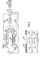
- a microprocessor 2 is programmed so as to deliver in operation control signals via a line 4 causing a radiation source 6, such as a Xenon-filled gas discharge lamp to flash at intervals.
- a radiation source 6 such as a Xenon-filled gas discharge lamp
- the intervals may be of the order of 15 ms. and the duration of each radiation flash may be of the order of 10 microseconds.
- a measurement optical path 8 and a reference optical path 10 are defined by suitable optical components forming no part of the present invention, in any manner which is suitable, such being known.
- Each flash of radiation on the reference path 10 is received by a reference channel 12 and converted to a corresponding electrical pulse signal which appears at the output 14 of that channel.
- On the measurement optical path 8, each flash of radiation from source 6 is incident upon a sample indicated at 16. In the case of a spectro- fluorimeter, this causes the sample 16 to emit a corresponding flash of fluorescent radiation 18 which is received by the measurement channel 12',and converted to a corresponding electrical pulse signal at the output 14' of that channel.
- the geometry of the measurement optical path is such that the measurement channel 12' cannot receive any radiation direct from source 6, but only radiation which has emanated from the sample 16. Filters may be placed in the optical paths to restrict measurement to a desired wavelength band.
- Microprocessor 2 is programmed so as to cause source 6 to generate a succession of a predetermined number (for example 48) of flashes as illustrated at 20 in Figure 2, and then hold the source 6 inactive during an equal period of time illustrated at 22, and then to repeat this cycle a predetermined number of times, for example 10 times.
- a predetermined number for example 48
- the reference and measurement channels 12 and 12' contain integrating circuitry, as will be explained further below, so that the quantities of radiation in the reference and measurement flashes received are progressively integrated throughout the duration of the initial succession of pulses 20, as indicated approximately by the ramp waveforms R (reference) and M (measurement) in Figure 2, to the final integrated values indicated at M 1 and R 1 at the end of the succession of pulses 20.
- Microprocessor 2 is programmed so as to then open a gate 24' by means of a control signal on line 26' to gate the integral output signal M 1 from output 14' to analogue-to-digital converter 28, the output of which is then stored in digital form in microprocessor 2, the integrator of measurement channel 12' being also reset to zero by means of the control signal on line 26'.
- microprocessor 2 causes the integral output R 1 on line 14 to be similarly converted to digital form and stored in the microprocessor by means of a control signal on line 26 operating gate 24 and, also, resetting of the integrator in reference channel 12.
- the reference and measurement channels 12 and 12' again carry out their integrating function but without flashes being generated by source 6. . Consequently, the integrated outputs build up as indicated at M' and R' to final values M' 1 and R' l indicative of the amount of unwanted signal, whether optical or electrical in origin, which has been developed in each of the two channels during the time period 22. These values are then transferred through to the microprocessor 2 in the manner which has already been described, and the microprocessor then computes the value:
- the lower line of this expression will represent the integrated amount of radiation received in reference channel 12 during time period 20 due solely to radiation flashes from source 6, and the top line would represent the integrated amount of fluorescent radiation 18, received solely from the sample 16, the ratio between the two then representing the degree of fluorescent activity of the sample 16 after taking into account the effect of the fluctuations in intensity of the radiation output from source 6.
- the microprocessor 2 is programmed so as to carry out the cycle a predetermined number (for example 10) of times, sum the results, divide by the total number of flashes in that number of cycles and then display the final average on a display unit 30.
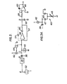
- the circuitry of Figure 3 is present in each of the channels 12 and 12'.
- a photomultiplier tube 32 arranged to receive the flash of radiation either direct from the source 6 or from the sample 16. Its putput pulses, in response to the received radiation flashes, are illustrated in waveform A of Figure 4 where it can be seen that the complete output signal also includes a substantially D.C. component, of relatively low level, to which dark current in the photomultiplier tube, stray light, and in the case of the measurement channel, phosphorescence of the sample, may contribute.
- This signal is applied to amplifier 36 to whose output a capacitor 38 is series-connected.
- a clamping circuit 40 is employed, which behaves as though it were a perfect diode orientated as shown in Figure 3. This alone would prevent the output side of capacitor 38 from going positive, but could not prevent it from drifting negative relative to zero volts.
- a current source 42 is provided to supply a current at least sufficient to compensate for the maximum voltage drift rate on capacitor 38. Any current (and at times this may be the entire current) surplus to that needed to keep the capacitor voltage up to zero simply flows away through circuit 40. This arrangement clamps the output of capacitor 38 to ground and holds the base line of the output pulse substantially at zero volts as illustrated in waveform C' of Figure 4.
- comparator 44 one of whose inputs is connected to circuit 40 and the other of whose inputs is connected to ground.
- the output of the comparator is employed to control the amount of current being provided by the current source 42.
- comparator 44 senses the presence of a pulse from capacitor 38, it reduces the current from source 42 to a low level, or possibly zero, so that distortion of the pulse waveform by such current, as illustrated at C' is avoided and the top of the pulse remains square, or very substantially so. Termination of the pulse is also sensed by the comparator, the output of which then re-adjusts the current source 42 to provide current to circuit 40 thereby holding its "anode” accurately at zero volts.
- FIG. 3A An example of a passive clamping circuit 40 is shown in Figure 3A.
- a variable resistor 45 is set so that the current through it is twice the current normally delivered by source 42. The circuit will then operate to hold the anode of diode 47 at the same voltage as that applied to the anode of diode 49 (in the illustrated example, zero volts).
- Various other circuits, including active circuits, are known for similarly acting as perfect diodes.
- the next circuit section consists of an operational amplifier 46 to the non-inverting input of which the signal from capacitor 38 is applied, diode 48 and a feedback loop 52 from diode 48 to the inverting input of amplifier 46.
- This arrangement functions as a substantially perfect diode and to facilitate explanation, a diode is illustrated at 54, which will be assumed to be perfect, and the equivalent of components 46, 48 and 52.
- Negative-going pulse C is transmitted through diode 54 and charges a capacitor 56 to a voltage equal to the amplitude of pulse C. The voltage on capacitor 56 remains at this level throughout the duration of pulse C as can be seen from waveform D in Figure 4.
- diode 54 On termination of the pulse, diode 54 becomes reverse-biased and capacitor 56 can discharge only through a resistor 58 and the input of integrating amplifier 60, so that it takes a substantial period of time to completely discharge.
- the waveform D is being applied as the input signal to the integrating amplifier 60, which is provided with capacitor 62 in its negative feedback path, so that the integral of the input signal will be substantially greater than it would have been had pulse C been applied to the input of the amplifier 60, owing to the effective lengthening of pulse C by the preceding stage of the circuitry.
- This pulse-stretching arrangement has two advantages.
- the circuit components may be chosen so that pulse D occupies half or even more of the interval between pulses, thereby suppressing a very substantial part of the noise which might otherwise be present at the integrator input.
- Figure 5 shows alternative circuitry for use in channels 12 and 12'.
- the A.C. coupled amplifier and its output clamping circuit are omitted and replaced by a D.C. amplifier 64.
- Its output is coupled directly to pulse-lengthening circuit 66 which may be the same as circuit 46, 48, 52, 56, 58 of Figure 3 which as before is connected to integrating amplifier 60, 62.
- pulse-lengthening circuit 66 which may be the same as circuit 46, 48, 52, 56, 58 of Figure 3 which as before is connected to integrating amplifier 60, 62. Since amplifier 64 will not filter out D.C. components of its input signal, these will contribute to the eventual integrated output signal of amplifier 60, 62 (M 1 in Figure 2). This would be a source of very substantial error in view of the length of the dark intervals compared with the flashes. It is therefore necessary to compensate by integrating also.
- an alternative source of radiation as an origin for the measured flashes would be a continuously operated tungsten/halogen lamp combined with a shutter or chopper or the equivalent to direct light from the source only intermittently on to the sample, or into the reference channel input.
Landscapes
- Physics & Mathematics (AREA)
- General Physics & Mathematics (AREA)
- Spectroscopy & Molecular Physics (AREA)
- Measurement Of Radiation (AREA)
- Investigating, Analyzing Materials By Fluorescence Or Luminescence (AREA)
Applications Claiming Priority (2)
| Application Number | Priority Date | Filing Date | Title |
|---|---|---|---|
| GB8039316A GB2089971A (en) | 1980-12-08 | 1980-12-08 | Apparatus for deriving an electrical signal from a radiation flash |
| GB8039316 | 1980-12-08 |
Publications (1)
| Publication Number | Publication Date |
|---|---|
| EP0055027A2 true EP0055027A2 (fr) | 1982-06-30 |
Family
ID=10517838
Family Applications (1)
| Application Number | Title | Priority Date | Filing Date |
|---|---|---|---|
| EP19810305477 Withdrawn EP0055027A2 (fr) | 1980-12-08 | 1981-11-19 | Dispositif pour l'obtention d'un signal électrique à partir d'un éclair de rayonnement, et instruments comportant un tel dispositif |
Country Status (3)
| Country | Link |
|---|---|
| EP (1) | EP0055027A2 (fr) |
| JP (1) | JPS57120877A (fr) |
| GB (1) | GB2089971A (fr) |
Cited By (5)
| Publication number | Priority date | Publication date | Assignee | Title |
|---|---|---|---|---|
| EP0440956A3 (en) * | 1989-12-20 | 1992-04-01 | Kabushiki Kaisha Topcon | Method and apparatus of photodetection |
| EP0529176A1 (fr) * | 1991-08-26 | 1993-03-03 | Gretag Imaging Ag | Procédé et dispositif pour mesurer de petites quantités de lumière |
| EP0953831A3 (fr) * | 1998-04-27 | 2000-09-13 | The Perkin-Elmer Corporation | Instrument spectroscopique piloté par ordinateur et calculateur associé |
| WO2022150192A1 (fr) * | 2021-01-06 | 2022-07-14 | Crosstex International, Inc. | Lecteur d'indicateur biologique, système et procédés d'utilisation |
| CN115398203A (zh) * | 2020-03-31 | 2022-11-25 | Msa技术有限公司 | 具有同步闪光检测的开路气体检测器 |
Families Citing this family (4)
| Publication number | Priority date | Publication date | Assignee | Title |
|---|---|---|---|---|
| GB8630136D0 (en) * | 1986-12-17 | 1987-01-28 | Grand Metropolitan Innovation | Luminometer apparatus |
| US5091653A (en) * | 1987-12-01 | 1992-02-25 | Quantex Corporation | Fiber optic dosimeter using electron trapping materials employing technique for eliminating background fluorescence |
| JP2000500875A (ja) * | 1996-09-16 | 2000-01-25 | バリアン・オーストラリア・ピーテイワイ・リミテツド | 改良された分光光度計 |
| US6197254B1 (en) | 1999-01-11 | 2001-03-06 | International Food Protection | Self-contained assaying apparatus |
-
1980
- 1980-12-08 GB GB8039316A patent/GB2089971A/en not_active Withdrawn
-
1981
- 1981-11-19 EP EP19810305477 patent/EP0055027A2/fr not_active Withdrawn
- 1981-12-08 JP JP19642681A patent/JPS57120877A/ja active Pending
Cited By (9)
| Publication number | Priority date | Publication date | Assignee | Title |
|---|---|---|---|---|
| EP0440956A3 (en) * | 1989-12-20 | 1992-04-01 | Kabushiki Kaisha Topcon | Method and apparatus of photodetection |
| US5196693A (en) * | 1989-12-20 | 1993-03-23 | Kabushiki Kaisha Topcon | Method and apparatus of photodetection with maximum signal holding means |
| EP0529176A1 (fr) * | 1991-08-26 | 1993-03-03 | Gretag Imaging Ag | Procédé et dispositif pour mesurer de petites quantités de lumière |
| US5307145A (en) * | 1991-08-26 | 1994-04-26 | Gretag Imaging, Ag | Process and apparatus for measuring small quantities of light |
| EP0953831A3 (fr) * | 1998-04-27 | 2000-09-13 | The Perkin-Elmer Corporation | Instrument spectroscopique piloté par ordinateur et calculateur associé |
| CN115398203A (zh) * | 2020-03-31 | 2022-11-25 | Msa技术有限公司 | 具有同步闪光检测的开路气体检测器 |
| CN115398203B (zh) * | 2020-03-31 | 2025-12-05 | Msa技术有限公司 | 具有同步闪光检测的开路气体检测器 |
| WO2022150192A1 (fr) * | 2021-01-06 | 2022-07-14 | Crosstex International, Inc. | Lecteur d'indicateur biologique, système et procédés d'utilisation |
| US12616769B2 (en) | 2021-01-06 | 2026-05-05 | Crosstex International, Inc. | Biological indicator reader with graphical user interface and methods of use |
Also Published As
| Publication number | Publication date |
|---|---|
| GB2089971A (en) | 1982-06-30 |
| JPS57120877A (en) | 1982-07-28 |
Similar Documents
| Publication | Publication Date | Title |
|---|---|---|
| US5463467A (en) | Light source pulsed with irregular pulse sequence in analog photometric signal evaluation for a test carrier analysis system | |
| EP0846333A1 (fr) | Detection synchrone pour detecteurs photoconducteurs | |
| WO1997017829B1 (fr) | Dispositif d'essai de composants a tension variable | |
| GB2089971A (en) | Apparatus for deriving an electrical signal from a radiation flash | |
| US11709185B2 (en) | Amplification interface, and corresponding measurement system and method for calibrating an amplification interface | |
| EP0470286B1 (fr) | Récepteur de signal à détection de niveau | |
| NL8402292A (nl) | Werkwijze en inrichting voor het automatisch stabiliseren van een scintillatiedetector. | |
| FI76454B (fi) | Samplings- och fasthaollningsstroemkrets speciellt foer smao signaler. | |
| JPS636802B2 (fr) | ||
| US10393892B2 (en) | X-ray detection circuit for a dental radiology sensor | |
| US4868573A (en) | Line frequency slaved voltage-to-frequency converter system | |
| US4666301A (en) | Radiation responsive integrating amplifier | |
| EP0238748B1 (fr) | Echantillonneur d'onde courante | |
| JP3008621B2 (ja) | 放射線測定装置 | |
| EP0143854A1 (fr) | Dispositif eliminant les images fantomes | |
| US5028788A (en) | X-ray sensor array | |
| GB2054297A (en) | Phase comparison circuit arrangement | |
| JP2577386B2 (ja) | 放射線エネルギスペクトル測定装置 | |
| US4829240A (en) | Secondary electron measuring circuit | |
| US4500205A (en) | Spectrophotometer | |
| US4545681A (en) | Method and apparatus for controlling measurement in a spectrophotometer | |
| US6411380B1 (en) | Detection device for a spectrophotometer | |
| JPS6039974B2 (ja) | 光学的検査 | |
| SU949346A1 (ru) | Устройство дл регистрации световых импульсов | |
| JPH01163632A (ja) | 測光回路 |
Legal Events
| Date | Code | Title | Description |
|---|---|---|---|
| PUAI | Public reference made under article 153(3) epc to a published international application that has entered the european phase |
Free format text: ORIGINAL CODE: 0009012 |
|
| AK | Designated contracting states |
Designated state(s): BE DE FR IT NL |
|
| STAA | Information on the status of an ep patent application or granted ep patent |
Free format text: STATUS: THE APPLICATION HAS BEEN WITHDRAWN |
|
| 18W | Application withdrawn |
Withdrawal date: 19840124 |
|
| RIN1 | Information on inventor provided before grant (corrected) |
Inventor name: NIXON, DENNIS WILLIAM |