EP0055571A2 - Circuit intégré du type ECL - Google Patents
Circuit intégré du type ECL Download PDFInfo
- Publication number
- EP0055571A2 EP0055571A2 EP81305983A EP81305983A EP0055571A2 EP 0055571 A2 EP0055571 A2 EP 0055571A2 EP 81305983 A EP81305983 A EP 81305983A EP 81305983 A EP81305983 A EP 81305983A EP 0055571 A2 EP0055571 A2 EP 0055571A2
- Authority
- EP
- European Patent Office
- Prior art keywords
- emitter
- ecl
- circuit
- test
- resistor
- Prior art date
- Legal status (The legal status is an assumption and is not a legal conclusion. Google has not performed a legal analysis and makes no representation as to the accuracy of the status listed.)
- Granted
Links
Images



Classifications
-
- H—ELECTRICITY
- H03—ELECTRONIC CIRCUITRY
- H03K—PULSE TECHNIQUE
- H03K19/00—Logic circuits, i.e. having at least two inputs acting on one output; Inverting circuits
- H03K19/003—Modifications for increasing the reliability for protection
- H03K19/00307—Modifications for increasing the reliability for protection in bipolar transistor circuits
-
- G—PHYSICS
- G01—MEASURING; TESTING
- G01R—MEASURING ELECTRIC VARIABLES; MEASURING MAGNETIC VARIABLES
- G01R31/00—Arrangements for testing electric properties; Arrangements for locating electric faults; Arrangements for electrical testing characterised by what is being tested not provided for elsewhere
- G01R31/28—Testing of electronic circuits, e.g. by signal tracer
- G01R31/316—Testing of analog circuits
-
- H—ELECTRICITY
- H03—ELECTRONIC CIRCUITRY
- H03K—PULSE TECHNIQUE
- H03K19/00—Logic circuits, i.e. having at least two inputs acting on one output; Inverting circuits
- H03K19/02—Logic circuits, i.e. having at least two inputs acting on one output; Inverting circuits using specified components
- H03K19/08—Logic circuits, i.e. having at least two inputs acting on one output; Inverting circuits using specified components using semiconductor devices
- H03K19/082—Logic circuits, i.e. having at least two inputs acting on one output; Inverting circuits using specified components using semiconductor devices using bipolar transistors
- H03K19/086—Emitter coupled logic
Definitions
- the present invention relates to an ECL (Emitter Coupled Logic) integrated circuit including one or a plurality of individual ECL circuits the or each of which comprises an emitter-follower transistor as an output stage. It particularly relates to the ability to test such a circuit in order to detect poor dynamic function.
- ECL Electrode Coupled Logic
- An individual ECL circuit whose fundamental element is an ECL gate in which emitters of a pair of transistors are connected with each other, and a reference voltage is applied to the base of one of the transistors with an input signal being applied to the base of the other thereof, often supplies its output OUT through an EF (emitter-follower) transistor as shown in Fig. 1.
- EF emitter-follower
- a base input of EF transistor Q EF is a collector output of an ECL gate which is not shown.
- the output stage of this ECL circuit is provided by connecting the emitter of transistor Q EF to an appropriate voltage V T through a pull-down resistor R T .
- connection between the emitter of transistor Q EF and the resistor R T is cut or broken at a point A, for example, in such a circuit the arrangement of resistor R T becomes ineffective. This accident may be caused when the contact window for the resistor R T is not opened, when the pattern of the resistor R T is broken in the path thereof, or when wiring is broken.
- An accident of this type is usually detected by a dynamic function test using a predetermined repetition freqency.
- the repetition frequency is low, however, the poor dynamic circuit function can sometimes not be detected.
- a conventional ECL circuit has an input characteristic as shown in Fig. 2 and H (high) level can be distinguished from L (low) level with a threshold voltage Vth of about - 1.3V interposed between them.
- P H represents a point at which H operation is usually carried out
- P L a point at which L operation is usually carried out.
- a cut of connection at point A is detected by such phenomenon that the level of output OUT will not drop lower than a certain voltage. This is natural when the emitter of transistor Q EF shown in Fig. 1 is kept open-circuit. However, said emitter is usually connected to other leads and arranged inside an integrated circuit IC (for example, combination logic circuit MLC shown in Fig.
- a solid line (b) represents the voltage of output OUT under the condition that the resistor R T is correctly connected without any break at point A.
- P 1 in Fig. 2 represents a point at which input voltage corresponding to that denoted by the broken line (a) in Fig. 3 is reduced to the lowest lower than Vth by input current applied to the subsequent stage.
- the repetition frequency employed in a tester may therefore be increased to overcome the problem, but the fundamental clock of future ultra-large-sized electronic computers is expected to have high frequency of about 100-200 MHz. When atester which can cover such a computer can not be obtained, it is impossible to carry out a satisfactory high frequency dynamic function test.
- the repetition frequency employed as the test frequency which is now put to practical use ranges from 10MHz to 20MHz at maximum, and that of the test frequency employed by the testers which are now manufactured for . trial, ranges from 50MHz to 100MHz.
- FIG. 5B is a pulse timing chart showing the operation of the ECL integrated circuit shown in Fig. 5A by means of outputs Q1 - Q3 of D-type flip-flops D-FF1, D-FF2 and D-FF3, clock CL, and input data DATA.
- the flip-flop D-FF1 takes-in the value of input data DATA, e.g. H level, in response to a first clock pulse CL1.
- the combination logic circuit MLC is a buffer/inverter circuit shown in Fig. 5C, for example, the flip-flop D-FF1 takes in L level in response to a next clock pulse CL2, while flip-flops D-FF2 and D-FF3 take-in outputs E2 and E3 of the combination logic circuit MLC, e.g.
- an ECL integrated circuit comprising at least one ECL circuit which comprises an emitter-follower transistor at the output and a pull-down means connected to said emitter-follower transistor, characterised in that a test circuit is arranged on a line extending from the output of said emitter-follower transistor to a subsequent circuit so as to cause auxiliary current to flow at the time of a test, said auxiliary current having a value smaller than the current normally flowing to said pull-down means but larger than the input current flowing to said subsequent circuit.
- an ECL integrated circuit comprising one or a plurality of ECL circuits the or each of which comprises an emitter-follower transistor at the output side and a pull-down resistor coupled to said emitter-follower transistor, characterized in that a test circuit is coupled to a line extending from the output of said emitter-follower transistor to a subsequent circuit so as to cause auxiliary current to flow in said line at the time of a testing, said test circuit including a connection of a resistor and a diode connected in series with each other, and a test terminal at the end of this connection opposite to the line end.
- an ECL integrated circuit comprising one or a plurality of ECL circuits the or each of which comprises an emitter-follower transistor at the output side and a pull-down resistor coupled to said emitter-follower transistor, characterised in that a test circuit is coupled to a line extending from the output of said emitter-follower transistor to a subsequent circuit so as to cause auxiliary current to flow at the time of a testing, said test circuit including a connection of a resistor and a transistor whose collector is connected to a power source terminal, whose emitter is connected via said resistor to said line extending from the output of said emitter-follower transistor to said subsequent circuit, and whose base is connected to a test terminal.
- a testing circuit TC to or through which auxiliary current I, smaller than the current usually flowing to the pull-down resistor R T , but larger than the sum of the input current flowing to the ECL circuits ECL 2 , ECL 3 , ----- as subsequent stages, is allowed to flow only at the time of test, is connected to a line L which extends from the emitter output of EF transistor Q EF in the ECL circuit ECL 1 , to the ECL circuits ECL 2 , ECL 3 , ----- as the subsequent stages.
- the testing circuit TC employed in this embodiment includes a diode D and a pull-up resistor R PU , connected in series between a testing terminal T lead-out outside an IC chip, and the line L, said diode D serving to prevent the backward flow of current.
- a testing circuit TC of is arranged at the output stage of each/ECL circuits ECL 1 , ECL 2 , etc. as shown in Fig. 7.
- the test terminal T is usually connected to a lowest potential V EE or VT, and is caused to be connected to a high potential V CC , for example, at the time of test. Since the test terminal.T is arranged as described above, no current consumption is normally caused in the testing circuit TC, and no problem that the ECL circuits are influenced by one another is caused at the time of usual or normal operation of the ECL integrated circuit.
- V CC voltage CC
- current 1 tends to flow corresponding to emitter potential of transistor Q EF . If the emitter-follower circuit EF is normal without any disconnection at point A, little current I flows when the input of transistor Q EF is at H level, but flows to the resistor R T when said output is at L level. Therefore, H and L level outputs of ECL circuit ECL 1 are transmitted to the subsequent stage as they are.
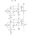
- Fig. 8 is a circuit diagram showing a second embodiment of the present invention employed in two input OR circuits.
- Inputs of transistors T 1A and T 2A are bases thereof, and collectors thereof are connected via a resistor to a power source V CC .
- the collectors thereof are also connected to the base of a transistor T 5A whose collector is connected to the power source V CC .
- the emitter of transistor T 5A is connected via a resistor R 3A to a power source V T and also to an output terminal OUT.,.
- the emitter of a transistor T 6A whose collector is connected to the power source V CC is connected via a resistor R 4A to the emitter of transistor T 5A .
- the emitter of transistor T 3A whose collector is connected to the power source V CC is connected to emitters of transistors T 1A and T 2A and is also connected via a transistor T 4A and a resistor R 2A to a power source VEE.
- a power source V BB To the base of transistor T 3A is connected a power source V BB while to the base of transistor T 4A a power source V CS is-connected.
- the power source V CC serves as a power source for supplying operating current
- the power source V T as a terminal power source
- the power source V BB as a power source for supplying reference voltage
- the power source V CS as a power source for applying constant bias voltage to the transistor T 4A'
- the transistor T 6A and resistor R 4A operate similarly to the diode D and resistor R PU shown in Fig. 6. Namely, voltage applied to a test terminal TEST is turned ON and thevoltage of power source V CC is consequently applied to one terminal of resistor R 4A' A circuit connected to an output terminal OUT 2 , is the same in arrangement as that just described and connected to the output terminal OUT 1 .
- the bases of the transistors T 6A a nd T 6B in these circuits, these circuits being connected to the output terminals OUT-, and OUT 2 , respectively, are connected to the test terminal TEST.
- the The circuit shown in Fig. 8 is substantially/same as that shown in Fig. 6.except that current flowing into the test terminal TEST is different in value.
- the current flowing to the resistor flows from the test terminal T in Fig. 6, but the value of the current flowing in the second embodiment shown in Fig. 8 may be enough.if it reaches about 1 per current amplifying ratio of transistor T 6A , because the ON/OFF action of. the transistor is employed.
- V CC is OV or ground voltage
- the resistor R 3A is 2K Ohm, and R 4A 3K Ohm.
- H level -V OH is - 0.8V and L level V OL -1.2V.
- current I R3L * flowing through R 3A is.
- V BE (T 6A ) represents the voltage between the emitter and base of transistor T 6A and is about 0.8V.
- collector current Ic of transistor T 4A is 0.3mA, and that h FE of transistor at the subsequent stage is 100, base current I B at the subsequent stage is:
- Fig. 9 is a circuit diagram showing a third embodiment of the present invention.
- Resistors R EE and R T are used as pull-down means for the emitter-follower in the first embodiment shown in Fig. 6, but transistors Q L ', Q L " and resistors R L ', R L " are employed in the third embodiment.
- the principle according to which the circuit is operated is the same as that in the first embodiment shown in Fig. 6.
- Bias voltage V x is applied to the bases of transistors Q L , and Q L " in this case.
- Both of resistors R EE and R T in Fig. 6 are replaced by transistors Q L ', Q L " and resistors R L ', R L " in Fig.
- resistors R EE and R T may be used together with any one of transistors Q L ', Q L " and the corresponding resistor R Ll or R L " in some cases.
- the resistor R EE may be used together with the transistor Q L " and resistor R L "
- the resistor R T may be used together with the transistor Q Ll and resistor R L '.
- Fig. 10 is a circuit diagram showing a fourth embodiment of the present-invention.
- the test terminal T must be connected via the resistor to the power source V T or V EE .
- the resistor is arranged inside the circuit in the case of the fourth embodiment shown in Fig. 10, thus enabling the operator to use the circuit with the test terminal opened.
- the incorrect dynamic function of a circuit which will follow malfunction at a time of normal use can be detected by a function test in which is employed a repetition frequency lower than the operating frequency employed for normal use.
Landscapes
- Engineering & Computer Science (AREA)
- Physics & Mathematics (AREA)
- General Engineering & Computer Science (AREA)
- Computer Hardware Design (AREA)
- Computing Systems (AREA)
- Mathematical Physics (AREA)
- Power Engineering (AREA)
- General Physics & Mathematics (AREA)
- Logic Circuits (AREA)
- Testing Or Measuring Of Semiconductors Or The Like (AREA)
- Bipolar Transistors (AREA)
- Tests Of Electronic Circuits (AREA)
Applications Claiming Priority (2)
| Application Number | Priority Date | Filing Date | Title |
|---|---|---|---|
| JP184563/80 | 1980-12-25 | ||
| JP55184563A JPS57107637A (en) | 1980-12-25 | 1980-12-25 | Ecl integrated circuit |
Publications (3)
| Publication Number | Publication Date |
|---|---|
| EP0055571A2 true EP0055571A2 (fr) | 1982-07-07 |
| EP0055571A3 EP0055571A3 (en) | 1982-12-01 |
| EP0055571B1 EP0055571B1 (fr) | 1985-03-20 |
Family
ID=16155390
Family Applications (1)
| Application Number | Title | Priority Date | Filing Date |
|---|---|---|---|
| EP81305983A Expired EP0055571B1 (fr) | 1980-12-25 | 1981-12-21 | Circuit intégré du type ECL |
Country Status (5)
| Country | Link |
|---|---|
| US (1) | US4410816A (fr) |
| EP (1) | EP0055571B1 (fr) |
| JP (1) | JPS57107637A (fr) |
| DE (1) | DE3169482D1 (fr) |
| IE (1) | IE53052B1 (fr) |
Cited By (3)
| Publication number | Priority date | Publication date | Assignee | Title |
|---|---|---|---|---|
| EP0218794A1 (fr) * | 1985-07-29 | 1987-04-22 | International Business Machines Corporation | Circuit d'essai pour un interrupteur de type cascade différentiel pour tension |
| EP0369921A3 (fr) * | 1988-11-14 | 1991-10-23 | International Business Machines Corporation | Identification de défauts dans les circuits de logique à émetteurs couplés |
| EP0479515A3 (fr) * | 1990-10-01 | 1994-10-12 | Motorola Inc | Circuit pour détecter des défauts. |
Families Citing this family (13)
| Publication number | Priority date | Publication date | Assignee | Title |
|---|---|---|---|---|
| JPS57162838A (en) * | 1981-03-31 | 1982-10-06 | Fujitsu Ltd | Emitter coupling type logical circuit |
| JPS6065557A (ja) * | 1983-09-21 | 1985-04-15 | Fujitsu Ltd | 集積回路装置 |
| US4719418A (en) * | 1985-02-19 | 1988-01-12 | International Business Machines Corporation | Defect leakage screen system |
| JPS62146014A (ja) * | 1985-12-20 | 1987-06-30 | Nec Corp | エミツタ結合論理回路 |
| US4692641A (en) * | 1986-02-13 | 1987-09-08 | Burr-Brown Corporation | Level shifting circuitry for serial-to-parallel converter |
| US4682058A (en) * | 1986-07-03 | 1987-07-21 | Unisys Corporation | Three-state logic circuit for wire-ORing to a data bus |
| US4967151A (en) * | 1988-08-17 | 1990-10-30 | International Business Machines Corporation | Method and apparatus for detecting faults in differential current switching logic circuits |
| US4942358A (en) * | 1988-11-02 | 1990-07-17 | Motorola, Inc. | Integrated circuit option identification circuit and method |
| US5742179A (en) * | 1994-01-27 | 1998-04-21 | Dyna Logic Corporation | High speed programmable logic architecture |
| US5614844A (en) * | 1994-01-27 | 1997-03-25 | Dyna Logic Corporation | High speed programmable logic architecture |
| US5463332A (en) * | 1994-07-22 | 1995-10-31 | National Semiconductor Corporation | Multiple differential input ECL or/nor gate |
| US6246259B1 (en) | 1998-02-23 | 2001-06-12 | Xilinx, Inc. | High-speed programmable logic architecture having active CMOS device drivers |
| JP4447515B2 (ja) | 2005-06-08 | 2010-04-07 | トヨタ紡織株式会社 | 車両用シートの操作レバー配置構造 |
Family Cites Families (3)
| Publication number | Priority date | Publication date | Assignee | Title |
|---|---|---|---|---|
| US3430071A (en) * | 1965-04-05 | 1969-02-25 | Rca Corp | Logic circuit |
| US4074188A (en) * | 1975-08-01 | 1978-02-14 | Testline Instruments, Inc. | Low impedance fault detection system and method |
| JPS5931892B2 (ja) * | 1976-11-19 | 1984-08-04 | 日本電気株式会社 | 半導体集積回路 |
-
1980
- 1980-12-25 JP JP55184563A patent/JPS57107637A/ja active Granted
-
1981
- 1981-12-04 US US06/327,692 patent/US4410816A/en not_active Expired - Fee Related
- 1981-12-21 DE DE8181305983T patent/DE3169482D1/de not_active Expired
- 1981-12-21 EP EP81305983A patent/EP0055571B1/fr not_active Expired
- 1981-12-23 IE IE3065/81A patent/IE53052B1/en unknown
Cited By (3)
| Publication number | Priority date | Publication date | Assignee | Title |
|---|---|---|---|---|
| EP0218794A1 (fr) * | 1985-07-29 | 1987-04-22 | International Business Machines Corporation | Circuit d'essai pour un interrupteur de type cascade différentiel pour tension |
| EP0369921A3 (fr) * | 1988-11-14 | 1991-10-23 | International Business Machines Corporation | Identification de défauts dans les circuits de logique à émetteurs couplés |
| EP0479515A3 (fr) * | 1990-10-01 | 1994-10-12 | Motorola Inc | Circuit pour détecter des défauts. |
Also Published As
| Publication number | Publication date |
|---|---|
| EP0055571A3 (en) | 1982-12-01 |
| JPH0357651B2 (fr) | 1991-09-02 |
| JPS57107637A (en) | 1982-07-05 |
| US4410816A (en) | 1983-10-18 |
| IE813065L (en) | 1982-06-25 |
| EP0055571B1 (fr) | 1985-03-20 |
| DE3169482D1 (en) | 1985-04-25 |
| IE53052B1 (en) | 1988-05-25 |
Similar Documents
| Publication | Publication Date | Title |
|---|---|---|
| EP0055571B1 (fr) | Circuit intégré du type ECL | |
| US4527079A (en) | Integrated circuit device accepting inputs and providing outputs at the levels of different logic families | |
| KR950005016B1 (ko) | 논리회로 및 그것을 사용한 반도체 집적회로장치 | |
| KR100236876B1 (ko) | 신호의 스윙을 저감하는 cmos 회로 | |
| KR890004886B1 (ko) | 래치회로 | |
| EP0194134A2 (fr) | Circuit intégré à semi-conducteur | |
| CN112243569A (zh) | 半导体集成电路装置及电平位移电路 | |
| US5783947A (en) | Semiconductor integrated circuit | |
| EP0216756B1 (fr) | Circuit integre acceptant des signaux d'entree et produisant des signaux de sortie correspondant aux niveaux de differentes familles de logiques | |
| US6762632B1 (en) | Reset driver circuits and methods | |
| US6275055B1 (en) | Semiconductor integrated circuit | |
| KR100310883B1 (ko) | 입력회로 | |
| WO2009029284A1 (fr) | Circuit à paire différentielle | |
| KR930009151B1 (ko) | 화합물 반도체 논리회로와 바이폴라 트랜지스터회로 사이에 설치된 인터페이스 회로 | |
| EP0450453B1 (fr) | Circuit d'entrée BICMOS pour détecter des signaux hors du domaine ECL | |
| EP0448263A2 (fr) | Dispositif de circuit intégré à semi-conducteur ayant un circuit de test | |
| EP0366294B1 (fr) | Circuit de conversion de niveaux TTL-ECL | |
| EP0350943B1 (fr) | Circuit intégré semi-conducteur comprenant un circuit tampon de sortie | |
| CN117856767B (zh) | 一种施密特触发器 | |
| EP0616224A2 (fr) | Dispositif semi-conducteur et son procédé de déverminage | |
| KR0135017B1 (ko) | 저전력 출력 버퍼회로 | |
| JP2826504B2 (ja) | 半導体集積回路 | |
| JP3105808B2 (ja) | 半導体装置およびこの半導体装置のモード設定方法 | |
| JP2590346B2 (ja) | 半導体装置 | |
| JPS6144372A (ja) | 論理lsiの試験装置 |
Legal Events
| Date | Code | Title | Description |
|---|---|---|---|
| PUAI | Public reference made under article 153(3) epc to a published international application that has entered the european phase |
Free format text: ORIGINAL CODE: 0009012 |
|
| AK | Designated contracting states |
Designated state(s): DE FR GB NL |
|
| PUAL | Search report despatched |
Free format text: ORIGINAL CODE: 0009013 |
|
| AK | Designated contracting states |
Designated state(s): DE FR GB NL |
|
| 17P | Request for examination filed |
Effective date: 19821124 |
|
| GRAA | (expected) grant |
Free format text: ORIGINAL CODE: 0009210 |
|
| AK | Designated contracting states |
Designated state(s): DE FR GB NL |
|
| REF | Corresponds to: |
Ref document number: 3169482 Country of ref document: DE Date of ref document: 19850425 |
|
| ET | Fr: translation filed | ||
| PLBE | No opposition filed within time limit |
Free format text: ORIGINAL CODE: 0009261 |
|
| STAA | Information on the status of an ep patent application or granted ep patent |
Free format text: STATUS: NO OPPOSITION FILED WITHIN TIME LIMIT |
|
| 26N | No opposition filed | ||
| PGFP | Annual fee paid to national office [announced via postgrant information from national office to epo] |
Ref country code: NL Payment date: 19871231 Year of fee payment: 7 |
|
| PG25 | Lapsed in a contracting state [announced via postgrant information from national office to epo] |
Ref country code: GB Effective date: 19881221 |
|
| PG25 | Lapsed in a contracting state [announced via postgrant information from national office to epo] |
Ref country code: NL Effective date: 19890701 |
|
| NLV4 | Nl: lapsed or anulled due to non-payment of the annual fee | ||
| GBPC | Gb: european patent ceased through non-payment of renewal fee | ||
| PG25 | Lapsed in a contracting state [announced via postgrant information from national office to epo] |
Ref country code: FR Free format text: LAPSE BECAUSE OF NON-PAYMENT OF DUE FEES Effective date: 19890831 |
|
| PG25 | Lapsed in a contracting state [announced via postgrant information from national office to epo] |
Ref country code: DE Effective date: 19890901 |
|
| REG | Reference to a national code |
Ref country code: FR Ref legal event code: ST |