EP0055601A2 - Pufferschaltung - Google Patents
Pufferschaltung Download PDFInfo
- Publication number
- EP0055601A2 EP0055601A2 EP81306073A EP81306073A EP0055601A2 EP 0055601 A2 EP0055601 A2 EP 0055601A2 EP 81306073 A EP81306073 A EP 81306073A EP 81306073 A EP81306073 A EP 81306073A EP 0055601 A2 EP0055601 A2 EP 0055601A2
- Authority
- EP
- European Patent Office
- Prior art keywords
- transistor
- fet
- buffer circuit
- gate
- potential
- Prior art date
- Legal status (The legal status is an assumption and is not a legal conclusion. Google has not performed a legal analysis and makes no representation as to the accuracy of the status listed.)
- Granted
Links
Images


Classifications
-
- H—ELECTRICITY
- H03—ELECTRONIC CIRCUITRY
- H03K—PULSE TECHNIQUE
- H03K19/00—Logic circuits, i.e. having at least two inputs acting on one output; Inverting circuits
- H03K19/01—Modifications for accelerating switching
- H03K19/017—Modifications for accelerating switching in field-effect transistor circuits
- H03K19/01707—Modifications for accelerating switching in field-effect transistor circuits in asynchronous circuits
- H03K19/01714—Modifications for accelerating switching in field-effect transistor circuits in asynchronous circuits by bootstrapping, i.e. by positive feed-back
-
- H—ELECTRICITY
- H03—ELECTRONIC CIRCUITRY
- H03K—PULSE TECHNIQUE
- H03K5/00—Manipulating of pulses not covered by one of the other main groups of this subclass
- H03K5/01—Shaping pulses
- H03K5/02—Shaping pulses by amplifying
- H03K5/023—Shaping pulses by amplifying using field effect transistors
Definitions
- the present invention relates to a buffer circuit.
- the buffer circuit of the present invention is used as, for example, an inverter circuit which employs FETs.
- the standby mode method in which zero or only a minimum current flows in portions of the static memory circuit in the standby mode.
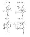
- the prior art buffer circuit of Fig. 1A comprises a depletion type FET 32 and an enhancement type FET 33.
- the input signal S such as a chip-select signal, is supplied to the gate 1 of FET 33 and the output signal S is produced at the point 6 at which the source and the gate of FET 32 and the drain of FET 33 are connected.
- the current flows through V cc , FET 32, FET 33 and V ss with the result that power down, i.e. the reduction of power dissipation, in the standby mode is not achieved.
- the prior art buffer circuit of Fig. 1B comprises enhancement type FETs 32 and 33, a capacitor 4 for bootstrap action and a diode connection FET 36.
- the prior art buffer circuit of Fig. 1C comprises an enhancement type FET 33, the gate of which receives an input signal S in , and another enhancement type FET 32, the gate of which receives the inverted signal S in of the signal S in .
- the potential of the output signal S out is reduced by the amount of V th , which is the threshold voltage of FET 32, with the result that the desired level of the high potential of the ouput signal S out cannot be attained.
- the prior art buffer circuit of Fig. 1D comprises FETs 31, 32 and 33, a capacitor 4 and an inverter 51.
- the input signal S. is supplied to the source of FET 31 and the input terminal of the inverter 51.
- the gate of FET 32 is connected to the drain of FET 31 and one electrode of the capacitor 4 while the gate of FET 33 is connected to the output terminal of the inverter 51.
- the circuit of F ig.
- Such a short duration pulse P may occur in the following cases. That is, for example, in the case where either the fall of the trailing edge of a first input signal of a two-input NAND gate circuit is too late or the rise of the leading edge of a second input signal of the two-input NAND gate circuit is too early. Also, for example, in the case where, as is usual in static memory circuits, the width of the signal pulse is.not selected to a predetermined amount in order to realize the simplification of the structure and the operation of the device.
- a buffer circuit comprising a first transistor, the source or the drain of which receives an input signal, a second transistor, the gate of which is connected to the drain or the source of said first transistor, said second transistor being adapted to carry out the bootstrap function, a third transistor which is connected in series with said second transistor, a signal which has the reverse phase of the phase of said input signal and is slightly delayed from said input signal being supplied to the gate of said third transistor, and an inverter connected to the output point at which said second and said third transistors are connected in series, said inverter inverting the potential of said output point and supplying said inverted potential to the gate of said first transistor.
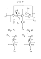
- FIG. 4 A buffer circuit in accordance with an embodiment of the present invention is illustrated in Fig. 4._
- the circuit of Fig. 4 comprises an input terminal 1, a first FET 31, a second FET 32, a third FET 33, a fourth FET 34, a fifth FET 35, a capacitor 4 for bootstrap effect, a first inverter 51, a second inverter 52, and an output terminal 6.
- FET 31, FET 32 and FET 33 are FETs of the enhancement type.
- FET 33 turns ON and hence low potential is produced at the output terminal 6.
- FET 33 turns OFF and hence high potential is produced at the output terminal.
- a high potential is applied to the gate of FET 32 due to the bootstrap effect of the capacitor 4 and FET 32 attains the completely conductive state.
- high potential of the output signal S out at the output terminal 6 can attain the potential V cc
- a signal S 51 which has the reverse phase of the phase of the input signal S in and is slightly delayed from the input signal S in , is supplied.
- the output signal S out is applied to the input terminal of the second inverter 52.
- the output signal S52 is the inverted signal of the signal S out .
- the signal S 52 is applied to the gate of the first FET 31.
- the fourth FET 34 is connected between the power source V cc and the gate circuit of the second FET 32.
- the fourth FET 34 operates to precharge the gate circuit of the second FET 32 when the power supply to the buffer circuit of Fig. 6 is switched on.
- the fifth FET 35 operates to supply charges to the output terminal 6 in order to prevent the potential of the output terminal 6 from being reduced due to a junction leakage.
- Figs. 7 and 8 The operation of the buffer circuit of Fig. 4 is illustrated in Figs. 7 and 8.
- the normal operation of the buffer circuit of Fig. 4 is illustrated in Fig. 7.
- Fig. 8 The operation of the buffer circuit of Fig. 4 in the case where a short duration pulse P occurs in the input signal S in is illustrated in Fig. 8.
- Fig. 8 (1) even when a short duration pulse P occurs in the input signal S in at the time t3 (Fig. 8, (1)), the charge at the gate circuit of the second FET 32 is not discharged and the potential of the gate circuit of the second FET 32 is maintained at a constant potential (Fig. 8, (2)), because the first transistor FET 31 is in the OFF state due to the low S 52 signal applied to the gate of the first FET 31.
- the potential S 51 varies from low level to high level and again to low level for a short period (Fig. 8, (3)).
- the FET 33 turns OFF and the potential Sout rises immediately to the potential V cc due to the normal bootstrap effect (Fig. 8, (4)).
- the short pulse P which occurs in the input signal S in does not exert a substantial influence on the waveform of the output signal S out (Fig. 8, (4)).
- Fig. ID there occurs hardly any power dissipation in the standby mode in the circuit of Fig. 4 in the case where a chip-select signal is used as an input signal.
- the inverter 51 comprises FET 511 and 512 connected in series.
- the input signal is supplied to the gate of FET 512.
- the output signal is produced at the terminal where the source and the gate of FET 511 and the drain of FET 512 are connected.
- the inverter 52 comprises FET 521 and 522 connected in series.
- the input signal is supplied to the gate of FET 522.
- the output signal is produced at the terminal where the source and the gate of FET 521 and the drain of.FET 522 are connected.
- the second input signal S 51 is the signal which is obtained by means of an inversion action on the first input signal S in of the inverter 51 and has a delay with respect to the input signal S in
- FET 34 and FET 35 are provided in the circuit of Fig. 4, it is possible to constitute embodiments of the present invention without FET 34 and FET 35.
Landscapes
- Physics & Mathematics (AREA)
- Engineering & Computer Science (AREA)
- Computer Hardware Design (AREA)
- Computing Systems (AREA)
- General Engineering & Computer Science (AREA)
- Mathematical Physics (AREA)
- Nonlinear Science (AREA)
- Logic Circuits (AREA)
- Electronic Switches (AREA)
Applications Claiming Priority (2)
| Application Number | Priority Date | Filing Date | Title |
|---|---|---|---|
| JP55183076A JPS609370B2 (ja) | 1980-12-24 | 1980-12-24 | バッファ回路 |
| JP183076/80 | 1980-12-24 |
Publications (3)
| Publication Number | Publication Date |
|---|---|
| EP0055601A2 true EP0055601A2 (de) | 1982-07-07 |
| EP0055601A3 EP0055601A3 (en) | 1982-08-04 |
| EP0055601B1 EP0055601B1 (de) | 1985-06-19 |
Family
ID=16129329
Family Applications (1)
| Application Number | Title | Priority Date | Filing Date |
|---|---|---|---|
| EP81306073A Expired EP0055601B1 (de) | 1980-12-24 | 1981-12-23 | Pufferschaltung |
Country Status (5)
| Country | Link |
|---|---|
| US (1) | US4449066A (de) |
| EP (1) | EP0055601B1 (de) |
| JP (1) | JPS609370B2 (de) |
| DE (1) | DE3171077D1 (de) |
| IE (1) | IE52383B1 (de) |
Cited By (4)
| Publication number | Priority date | Publication date | Assignee | Title |
|---|---|---|---|---|
| EP0101947A1 (de) * | 1982-07-28 | 1984-03-07 | Nec Corporation | Treiberschaltung |
| EP0137620A3 (en) * | 1983-08-17 | 1986-03-26 | American Telephone And Telegraph Company | Improvements in or relating to integrated circuits |
| DE4324651A1 (de) * | 1992-12-17 | 1994-06-23 | Mitsubishi Electric Corp | Boosting-Schaltung zum Betrieb in einem weiten Versorungsspannungsbereich sowie Halbleiterspeicher und integrierte Halbleiterschaltungsvorrichtung, die diese Schaltung benutzen |
| US8659532B2 (en) | 2001-04-27 | 2014-02-25 | Semiconductor Energy Laboratory Co., Ltd. | Semiconductor device |
Families Citing this family (19)
| Publication number | Priority date | Publication date | Assignee | Title |
|---|---|---|---|---|
| US4725746A (en) * | 1981-10-20 | 1988-02-16 | Kabushiki Kaisha Toshiba | MOSFET buffer circuit with an improved bootstrapping circuit |
| JPS58185091A (ja) * | 1982-04-24 | 1983-10-28 | Toshiba Corp | 昇圧電圧出力回路および昇圧電圧出力回路を備えたアドレスデコ−ド回路 |
| US4496852A (en) * | 1982-11-15 | 1985-01-29 | International Business Machines Corporation | Low power clock generator |
| US4617476A (en) * | 1984-10-16 | 1986-10-14 | Zilog, Inc. | High speed clocked, latched, and bootstrapped buffer |
| IT1185851B (it) * | 1985-08-02 | 1987-11-18 | Sgs Microelettronica Spa | Circuito di pilotaggio con boctstrap in tecnologia n-mos per carichi capacitivi |
| US4804870A (en) * | 1987-08-07 | 1989-02-14 | Signetics Corporation | Non-inverting, low power, high speed bootstrapped buffer |
| JPH01161963A (ja) * | 1987-12-17 | 1989-06-26 | Seiki Kogyo Kk | 書画像読取装置 |
| US5084634A (en) * | 1990-10-24 | 1992-01-28 | Burr-Brown Corporation | Dynamic input sampling switch for CDACS |
| US5359828A (en) * | 1993-09-30 | 1994-11-01 | Day John E | Post assembly |
| US6486816B2 (en) * | 2001-04-03 | 2002-11-26 | Texas Instruments Incorporated | CDAC operation at low supply voltages |
| KR100432652B1 (ko) * | 2002-08-01 | 2004-05-22 | 삼성에스디아이 주식회사 | 레벨 시프터 및 평판 표시 장치 |
| US7304502B2 (en) * | 2004-06-28 | 2007-12-04 | Samsung Sdi Co., Ltd | Level shifter and flat panel display comprising the same |
| TWI309922B (en) * | 2006-02-14 | 2009-05-11 | Au Optronics Corp | Bootstrap inverter circuit |
| KR101539667B1 (ko) * | 2008-06-18 | 2015-07-28 | 삼성전자주식회사 | 인버터 소자 및 그 동작 방법 |
| JP5672910B2 (ja) * | 2010-09-29 | 2015-02-18 | 大日本印刷株式会社 | 論理否定型電子回路 |
| JP2012078839A (ja) * | 2011-11-07 | 2012-04-19 | Semiconductor Energy Lab Co Ltd | 表示装置の駆動回路 |
| US9385718B1 (en) | 2013-10-18 | 2016-07-05 | Altera Corporation | Input-output buffer circuit with a gate bias generator |
| JP6628837B2 (ja) * | 2018-06-15 | 2020-01-15 | 株式会社半導体エネルギー研究所 | 電子機器 |
| EP3670354B1 (de) * | 2018-12-17 | 2022-05-11 | Goodrich Lighting Systems GmbH | Leuchtanordnung |
Family Cites Families (5)
| Publication number | Priority date | Publication date | Assignee | Title |
|---|---|---|---|---|
| US3906254A (en) * | 1974-08-05 | 1975-09-16 | Ibm | Complementary FET pulse level converter |
| DE2639555C2 (de) * | 1975-09-04 | 1985-07-04 | Plessey Overseas Ltd., Ilford, Essex | Elektrische integrierte Schaltung |
| US4080539A (en) * | 1976-11-10 | 1978-03-21 | Rca Corporation | Level shift circuit |
| GB1573771A (en) * | 1977-09-26 | 1980-08-28 | Philips Electronic Associated | Buffer circuit |
| US4307308A (en) * | 1979-11-19 | 1981-12-22 | Gte Laboratories Incorporated | Digital signal conversion circuit |
-
1980
- 1980-12-24 JP JP55183076A patent/JPS609370B2/ja not_active Expired
-
1981
- 1981-12-16 US US06/331,287 patent/US4449066A/en not_active Expired - Fee Related
- 1981-12-23 EP EP81306073A patent/EP0055601B1/de not_active Expired
- 1981-12-23 DE DE8181306073T patent/DE3171077D1/de not_active Expired
- 1981-12-23 IE IE3069/81A patent/IE52383B1/en not_active IP Right Cessation
Cited By (5)
| Publication number | Priority date | Publication date | Assignee | Title |
|---|---|---|---|---|
| EP0101947A1 (de) * | 1982-07-28 | 1984-03-07 | Nec Corporation | Treiberschaltung |
| EP0137620A3 (en) * | 1983-08-17 | 1986-03-26 | American Telephone And Telegraph Company | Improvements in or relating to integrated circuits |
| DE4324651A1 (de) * | 1992-12-17 | 1994-06-23 | Mitsubishi Electric Corp | Boosting-Schaltung zum Betrieb in einem weiten Versorungsspannungsbereich sowie Halbleiterspeicher und integrierte Halbleiterschaltungsvorrichtung, die diese Schaltung benutzen |
| US8659532B2 (en) | 2001-04-27 | 2014-02-25 | Semiconductor Energy Laboratory Co., Ltd. | Semiconductor device |
| US9136385B2 (en) | 2001-04-27 | 2015-09-15 | Semiconductor Energy Laboratory Co., Ltd. | Semiconductor device |
Also Published As
| Publication number | Publication date |
|---|---|
| IE813069L (en) | 1982-06-24 |
| IE52383B1 (en) | 1987-10-14 |
| JPS57106227A (en) | 1982-07-02 |
| JPS609370B2 (ja) | 1985-03-09 |
| DE3171077D1 (en) | 1985-07-25 |
| US4449066A (en) | 1984-05-15 |
| EP0055601A3 (en) | 1982-08-04 |
| EP0055601B1 (de) | 1985-06-19 |
Similar Documents
| Publication | Publication Date | Title |
|---|---|---|
| EP0055601A2 (de) | Pufferschaltung | |
| US4071783A (en) | Enhancement/depletion mode field effect transistor driver | |
| US5521547A (en) | Boost voltage generating circuit | |
| US5936443A (en) | Power-on reset signal generator for semiconductor device | |
| US5514994A (en) | Bootstrap circuit | |
| US4542310A (en) | CMOS bootstrapped pull up circuit | |
| US4574203A (en) | Clock generating circuit providing a boosted clock signal | |
| US4565932A (en) | High voltage circuit for use in programming memory circuits (EEPROMs) | |
| US4038567A (en) | Memory input signal buffer circuit | |
| US5184030A (en) | Back bias generating circuit | |
| US4276487A (en) | FET driver circuit with short switching times | |
| US3937983A (en) | Mos buffer circuit | |
| US4622479A (en) | Bootstrapped driver circuit for high speed applications | |
| US4894559A (en) | Buffer circuit operable with reduced power consumption | |
| EP0032017B1 (de) | Bootstrapschaltung | |
| US4587441A (en) | Interface circuit for signal generators with two non-overlapping phases | |
| US4239991A (en) | Clock voltage generator for semiconductor memory | |
| EP0063357B1 (de) | Treiberschaltung | |
| US4352996A (en) | IGFET Clock generator circuit employing MOS boatstrap capacitive drive | |
| US4468576A (en) | Inverter circuit having transistors operable in a shallow saturation region for avoiding fluctuation of electrical characteristics | |
| US4540898A (en) | Clocked buffer circuit using a self-bootstrapping transistor | |
| JP2000021179A (ja) | ブースト回路及びこれを用いた半導体装置 | |
| JP2527050B2 (ja) | 半導体メモリ用センスアンプ回路 | |
| US4611134A (en) | Bootstrap driving circuit | |
| JPH03283182A (ja) | 半導体昇圧回路 |
Legal Events
| Date | Code | Title | Description |
|---|---|---|---|
| PUAI | Public reference made under article 153(3) epc to a published international application that has entered the european phase |
Free format text: ORIGINAL CODE: 0009012 |
|
| PUAL | Search report despatched |
Free format text: ORIGINAL CODE: 0009013 |
|
| AK | Designated contracting states |
Designated state(s): DE FR GB NL |
|
| AK | Designated contracting states |
Designated state(s): DE FR GB NL |
|
| 17P | Request for examination filed |
Effective date: 19830124 |
|
| GRAA | (expected) grant |
Free format text: ORIGINAL CODE: 0009210 |
|
| AK | Designated contracting states |
Designated state(s): DE FR GB NL |
|
| REF | Corresponds to: |
Ref document number: 3171077 Country of ref document: DE Date of ref document: 19850725 |
|
| ET | Fr: translation filed | ||
| PLBE | No opposition filed within time limit |
Free format text: ORIGINAL CODE: 0009261 |
|
| STAA | Information on the status of an ep patent application or granted ep patent |
Free format text: STATUS: NO OPPOSITION FILED WITHIN TIME LIMIT |
|
| 26N | No opposition filed | ||
| PGFP | Annual fee paid to national office [announced via postgrant information from national office to epo] |
Ref country code: GB Payment date: 19921013 Year of fee payment: 12 |
|
| PGFP | Annual fee paid to national office [announced via postgrant information from national office to epo] |
Ref country code: FR Payment date: 19921221 Year of fee payment: 12 |
|
| PGFP | Annual fee paid to national office [announced via postgrant information from national office to epo] |
Ref country code: NL Payment date: 19921231 Year of fee payment: 12 |
|
| PGFP | Annual fee paid to national office [announced via postgrant information from national office to epo] |
Ref country code: DE Payment date: 19930226 Year of fee payment: 12 |
|
| PG25 | Lapsed in a contracting state [announced via postgrant information from national office to epo] |
Ref country code: GB Effective date: 19931223 |
|
| PG25 | Lapsed in a contracting state [announced via postgrant information from national office to epo] |
Ref country code: NL Effective date: 19940701 |
|
| NLV4 | Nl: lapsed or anulled due to non-payment of the annual fee | ||
| GBPC | Gb: european patent ceased through non-payment of renewal fee |
Effective date: 19931223 |
|
| PG25 | Lapsed in a contracting state [announced via postgrant information from national office to epo] |
Ref country code: FR Effective date: 19940831 |
|
| PG25 | Lapsed in a contracting state [announced via postgrant information from national office to epo] |
Ref country code: DE Effective date: 19940901 |
|
| REG | Reference to a national code |
Ref country code: FR Ref legal event code: ST |