EP0055672A1 - Annährungs- bzw. Anwesenheitsdetektorgerät des Zwei-Klemmen-Typs mit einer Versorgungsschaltung für gleichgerichteten Wechselstrom und einer Laststeuerung mit Schaltthyristoren - Google Patents
Annährungs- bzw. Anwesenheitsdetektorgerät des Zwei-Klemmen-Typs mit einer Versorgungsschaltung für gleichgerichteten Wechselstrom und einer Laststeuerung mit Schaltthyristoren Download PDFInfo
- Publication number
- EP0055672A1 EP0055672A1 EP81402075A EP81402075A EP0055672A1 EP 0055672 A1 EP0055672 A1 EP 0055672A1 EP 81402075 A EP81402075 A EP 81402075A EP 81402075 A EP81402075 A EP 81402075A EP 0055672 A1 EP0055672 A1 EP 0055672A1
- Authority
- EP
- European Patent Office
- Prior art keywords
- thyristor
- transistor
- semiconductor component
- series
- zener diode
- Prior art date
- Legal status (The legal status is an assumption and is not a legal conclusion. Google has not performed a legal analysis and makes no representation as to the accuracy of the status listed.)
- Granted
Links
- 239000004065 semiconductor Substances 0.000 claims abstract description 18
- 239000003990 capacitor Substances 0.000 claims abstract description 17
- 229920006395 saturated elastomer Polymers 0.000 claims abstract description 10
- 239000002699 waste material Substances 0.000 claims description 8
- 230000000903 blocking effect Effects 0.000 claims description 5
- 230000010287 polarization Effects 0.000 claims description 3
- 239000004020 conductor Substances 0.000 description 10
- 239000008186 active pharmaceutical agent Substances 0.000 description 3
- 230000000694 effects Effects 0.000 description 2
- 230000006378 damage Effects 0.000 description 1
- 238000010586 diagram Methods 0.000 description 1
- 238000005516 engineering process Methods 0.000 description 1
- 230000001939 inductive effect Effects 0.000 description 1
- 238000000034 method Methods 0.000 description 1
- 230000001681 protective effect Effects 0.000 description 1
- 238000009877 rendering Methods 0.000 description 1
- 238000009738 saturating Methods 0.000 description 1
Images
Classifications
-
- H—ELECTRICITY
- H03—ELECTRONIC CIRCUITRY
- H03K—PULSE TECHNIQUE
- H03K17/00—Electronic switching or gating, i.e. not by contact-making and –breaking
- H03K17/08—Modifications for protecting switching circuit against overcurrent or overvoltage
- H03K17/082—Modifications for protecting switching circuit against overcurrent or overvoltage by feedback from the output to the control circuit
- H03K17/0824—Modifications for protecting switching circuit against overcurrent or overvoltage by feedback from the output to the control circuit in thyristor switches
Definitions
- the invention relates to detector devices of the two-terminal type, supplied with alternating current and comprising a sensor associated with a control circuit, which are connected in series with the load to be controlled, and more particularly to supply devices, control of the output current and of protection against overloads or short-circuits, which such devices comprise.
- control of the load is frequently carried out by making at least one thyristor conductive when the sensor delivers a control signal, which causes the circulation in the load, through the circuit, of a current, called current of output, of sufficient intensity to control the load.
- These devices generally comprise, in addition to the sensor and the control circuit, means for rectifying the current used to power the device, a resistor, in series with the sensor-control circuit assembly and which is used to power the latter when the load is at rest, and a Zener diode, connected to the terminals of this together and in series with the thyristor in order to define a reference voltage.
- a disadvantage of the devices of the prior art lies in the fact that when the thyristor is made conductive, the resumption of the control thereof can only be done when the current flowing through it is close to zero. This does not ensure protection of the circuit when an overload or a short circuit occurs while a command command of the load is supplied by the sensor, and the thyristor is therefore conductive.
- the invention proposes to eliminate this drawback by providing the device with protective means mounted in series with the thyristor in order to control the current flowing through it, said means comprising a high gain semiconductor component (T 3 ) mounted in series with the thyristor, comprising an input (D) and a power output (S) and at least one control input (G), a transistor (T 2 ) connected in parallel between said control input (G) and the output of said semiconductor component (T 3 ) in such a way that said normally unsaturated transistor (T 2) becomes saturated when an overload or a short-circuit of load occurs and when saturation of said transistor (T 2 ) causes the blocking of the semiconductor component (T 3 ) and consequently the current in the thyristor (TH I ) is limited by R 7 and R 8 .
- the invention also proposes to use a second thyristor mounted in series with the protection means and in parallel on the thyristor unit and the Zener diode.
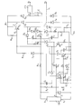
- the assembly shown in the single figure is supplied with alternating voltage via two supply terminals e l , e 2 connected to a full-wave rectifier bridge with diodes D 4 -D 7 by two supply conductors respectively v 1 and v 2 , on one of which is connected in series a load CH which can be for example a relay.
- the rectifier bridge supplies at its terminals a rectified voltage supplying the rest of the assembly via two supply conductors V DD (positive polarity) and V SS (negative polarity).
- a charge control sensor-circuit assembly comprising for example a photo-transistor having two positive supply terminals b 1 and negative b 2 and an output s.
- the negative terminal b 2 is directly connected to V SS , the positive terminal b 1 being connected to V DD via a resistor R 31, a Zener diode Z 1 being connected in parallel on the terminals b 1 b 2 and having its anode connected to the conductor of negative polarity and its cathode connected to the positive supply terminal.
- the output s is connected to the base of a transistor T l , for example of the NPN type, the emitter of which is connected to V SS and the collector is connected to V DD via a resistor R 2 , a bias resistor R 1 being mounted between the base of this transistor T 1 and V SS .
- the collector of transistor T 1 is connected to the trigger of a first thyristor TH 1 , the cathode of which is connected to V SS via and in the order in which they are cited with a light-emitting diode LED mounted with the same polarity. that the thyristor, used to signal the state at rest or in charge of CH, of a Zener diode Z 2 , mounted in opposition to the thyristor, with a resistance R 5 and a resistance R 11 .
- the anode of the thyristor TH 1 is connected to the emitter of a transistor, for example of the NPN, T 2 type, the base of which is polarized by a bridge of resistors R 7 and R 6 .
- Resistor R 7 is directly connected to V DD ; resistor R 6 is mounted in parallel on the base-emitter junction of transistor T 21 a delay capacitor C 2 is also mounted in parallel on this base-emitter junction.
- the collector of T 2 is connected to the gate of a transistor T 3 advantageously of the MOS type.
- the transistor T 3 is connected in series with a second thyristor TH 2 between the two supply conductors V DD and V SS , its train being connected to V DD and its source being connected both to the anode of TH 2 and to that of TH 1 ; the trigger of TH 2 is connected to the anode of Z 2 .
- the gate of transistor T 3 is biased through a resistor R 8 mounted between its gate and the conductor V DD and by means of a resistor R 10 connected in series with a first diode D 1 and a second diode D 2 mounted in the same direction, the anode of D 2 being connected to the cathode of Z 2 .
- the cathode of D 2 is also connected to the terminal b 1 via a resistor R 4 ; a capacitor C 1 serves as a supply tank for the CAP assembly and is mounted in parallel on the assembly constituted by the diode D 2 , the Zener diode Z 2 and the resistor R 5 .
- a resistor R 9 and a filter capacitor C 3 are connected in series between the two supply conductors V DD and V SS .
- a nonlinear resistor E is mounted between the AC power supply conductors v I and v 2 downstream of the load CH.
- a voltage V DS appears between the drain and the source of transistor T 3 ; this voltage is insufficient in the absence of overload, to bring the transistor T 2 in its saturated state, the values of the resistances, of bias of the transistor T 2 , R 6 and R 7 being chosen for this purpose.
- the thyristor TH 2 becomes non-conductive, and when the load current begins to increase again, the sequence: thyristor TH 1 conductor, charge of C l , thyristor TH 2 conductor, described above, is reproduced. This process has the effect of significantly reducing the average value of the waste voltage.
- the blocking of the transistor T 2 will be obtained, either by saturating the transistor T l , or by defusing the thyristor TH 1 , or finally by disconnecting one of the supply wires from the device.
- T 1 , T 2 associated with R 6 , R 7 , R 81 R 10 , C 1 and D1 therefore effectively protects the device in the event of an overload or short circuit when the load is ordered.
- the use of a MOS transistor makes it possible to produce a load control circuit consuming only a negligible current vis-à-vis the current necessary to control the load, therefore not disturbing the operation thereof.
- the gate current necessary to control the MOS transistor is of the order of a hundred nanoamperes (100 to 200 nA), while the current passing through the channel can reach intensities of the order of an ampere, which allows for a control and protection circuit in which the currents flowing are of very low intensity, therefore consuming a low energy, which is an advantage in this kind of device.
- the value of the resistor R 11 is chosen so that the potential difference across its terminals is high enough to cause the thyristor TH 2 to start when it is crossed by a current whose value is close of the admissible limit by the two components C 1 and DEL, the thyristor TH 2 deriving the current as described previously.
- the non-linear resistance E allows the protection of the device against overvoltages of inductive origin which can appear at the terminals of the load during the blocking of the transistor T 3 , when the load comprises inductances.
- the arrangement described above therefore makes it possible to limit the waste voltage in series with the load by the commissioning of a second thyristor, the current passing through the thyristors and the load being controlled by means of the control of the MOS transistor. .
- the use of this type of transistor in the circuit has the advantage of providing a control and protection circuit, which requires only very low current for its operation, which therefore does not risk influencing the operation of load.
- This arrangement also has the advantage of protecting the components for which the admissible current is lower than that for which the protection is designed, in the event of ignition on a load short circuit, by the commissioning of the second thyristor, this which has the effect of diverting the current, which could have destroyed them, through the latter.
- the assembly described may be subject to variant embodiments, without departing from the invention.
- it may include only one thyristor TH 1 , the thyristor TH 2 as well as the components R 5 , R 11 , C 1 , D 1 and R 10 then being deleted.
- Such an assembly will have the disadvantage of having a higher waste voltage than that obtained in the assembly of the figure.
- the protection of the assembly by reducing the current flowing in the assembly when it reached a certain threshold during an overload or a short-circuit of load is obtained thanks to the saturation of the transistor T 2 which causes the blocking of the transistor T 3 and thus reduces the current passing through the thyristor TH 1 to the value of saturation current of T 2 .
- the transistor T 3 of MOS technology can be replaced by a high-gain power Darlington circuit.
Landscapes
- Electronic Switches (AREA)
Applications Claiming Priority (2)
| Application Number | Priority Date | Filing Date | Title |
|---|---|---|---|
| FR8027870 | 1980-12-31 | ||
| FR8027870A FR2497423A1 (fr) | 1980-12-31 | 1980-12-31 | Appareil detecteur du type a deux bornes, comportant un circuit d'alimentation en courant alternatif redresse et de commande d'une charge a l'aide de thyristors de commutation |
Publications (2)
| Publication Number | Publication Date |
|---|---|
| EP0055672A1 true EP0055672A1 (de) | 1982-07-07 |
| EP0055672B1 EP0055672B1 (de) | 1985-02-13 |
Family
ID=9249678
Family Applications (1)
| Application Number | Title | Priority Date | Filing Date |
|---|---|---|---|
| EP81402075A Expired EP0055672B1 (de) | 1980-12-31 | 1981-12-24 | Annährungs- bzw. Anwesenheitsdetektorgerät des Zwei-Klemmen-Typs mit einer Versorgungsschaltung für gleichgerichteten Wechselstrom und einer Laststeuerung mit Schaltthyristoren |
Country Status (3)
| Country | Link |
|---|---|
| EP (1) | EP0055672B1 (de) |
| DE (1) | DE3168980D1 (de) |
| FR (1) | FR2497423A1 (de) |
Cited By (1)
| Publication number | Priority date | Publication date | Assignee | Title |
|---|---|---|---|---|
| JPS63501539A (ja) * | 1985-09-24 | 1988-06-09 | スクウエア− デイ− カンパニ− | 低リ−ク交流近接スイッチ回路 |
Citations (5)
| Publication number | Priority date | Publication date | Assignee | Title |
|---|---|---|---|---|
| FR2234711A1 (de) * | 1973-06-22 | 1975-01-17 | Buck Robert | |
| FR2348605A1 (fr) * | 1976-04-15 | 1977-11-10 | Buck Robert | Dispositif electronique de commutation perfectionne |
| DE2750992A1 (de) * | 1977-11-15 | 1979-05-17 | Hiss Eckart | Thyristor sicherheitsanordnung |
| DE2845553A1 (de) * | 1978-10-17 | 1980-04-24 | Licentia Gmbh | Schalter mit steuerbaren halbleiterventilen |
| FR2445075A1 (fr) * | 1978-12-20 | 1980-07-18 | Western Electric Co | Circuit de commutation de puissance |
Family Cites Families (1)
| Publication number | Priority date | Publication date | Assignee | Title |
|---|---|---|---|---|
| FR2457604A1 (fr) * | 1979-05-25 | 1980-12-19 | Telemecanique Electrique | Detecteur photo-electrique de la presence d'un objet, du type a deux fils |
-
1980
- 1980-12-31 FR FR8027870A patent/FR2497423A1/fr active Granted
-
1981
- 1981-12-24 DE DE8181402075T patent/DE3168980D1/de not_active Expired
- 1981-12-24 EP EP81402075A patent/EP0055672B1/de not_active Expired
Patent Citations (5)
| Publication number | Priority date | Publication date | Assignee | Title |
|---|---|---|---|---|
| FR2234711A1 (de) * | 1973-06-22 | 1975-01-17 | Buck Robert | |
| FR2348605A1 (fr) * | 1976-04-15 | 1977-11-10 | Buck Robert | Dispositif electronique de commutation perfectionne |
| DE2750992A1 (de) * | 1977-11-15 | 1979-05-17 | Hiss Eckart | Thyristor sicherheitsanordnung |
| DE2845553A1 (de) * | 1978-10-17 | 1980-04-24 | Licentia Gmbh | Schalter mit steuerbaren halbleiterventilen |
| FR2445075A1 (fr) * | 1978-12-20 | 1980-07-18 | Western Electric Co | Circuit de commutation de puissance |
Cited By (1)
| Publication number | Priority date | Publication date | Assignee | Title |
|---|---|---|---|---|
| JPS63501539A (ja) * | 1985-09-24 | 1988-06-09 | スクウエア− デイ− カンパニ− | 低リ−ク交流近接スイッチ回路 |
Also Published As
| Publication number | Publication date |
|---|---|
| DE3168980D1 (en) | 1985-03-28 |
| FR2497423B1 (de) | 1984-05-18 |
| EP0055672B1 (de) | 1985-02-13 |
| FR2497423A1 (fr) | 1982-07-02 |
Similar Documents
| Publication | Publication Date | Title |
|---|---|---|
| EP0055673B1 (de) | Mit gleichgerichtetem Wechselstrom bei einer über einen grossen Bereich schwankenden Spannung gespeistes Annäherungs- bzw. Anwesenheitsdetektorgerät mit Laststeuerung durch Schalthyristoren | |
| FR2567340A1 (fr) | Relais a semi-conducteur protege contre les surcharges de courant | |
| FR2693853A1 (fr) | Circuit de protection d'un composant de puissance contre des surtensions directes. | |
| FR2484740A1 (fr) | Circuit de protection pour un transistor de commutation et son procede de realisation | |
| FR2661574A1 (fr) | Circuit de relais a semiconducteurs a seuil de declenchement de surcharge compense en temperature. | |
| EP0635923A1 (de) | Schutzschaltung gegen Überspannungen hoher Energie mit geregelter Spannungsbegrenzung | |
| FR2547133A1 (fr) | Circuit destine a prevenir une dissipation excessive d'energie dans les dispositifs commutateurs de puissance | |
| FR2572600A1 (fr) | Stabilisateur electronique de tension, utilisable en particulier dans l'automobile, avec protection contre les surtensions transitoires de polarite opposee a celle du generateur | |
| CA1194588A (fr) | Circuit d'alimentation d'un contact de commande et son application a la commande d'une temporisation de repos d'un relais | |
| FR2619262A1 (fr) | Dispositif de protection d'un equipement contre les surtensions induites sur une ligne lui etant raccordee | |
| EP0055672B1 (de) | Annährungs- bzw. Anwesenheitsdetektorgerät des Zwei-Klemmen-Typs mit einer Versorgungsschaltung für gleichgerichteten Wechselstrom und einer Laststeuerung mit Schaltthyristoren | |
| FR2531580A1 (fr) | Circuit de protection contre la mise en court-circuit de l'enroulement d'excitation pour un alternateur a basse tension equipe d'un regulateur de tension, en particulier pour la construction automobile | |
| FR2556909A1 (fr) | Dispositif d'interface pour un poste telephonique | |
| EP0843412B1 (de) | Anwesenheitsdetektor mit einer stabilisierten Stromquelle | |
| FR3016751A1 (fr) | Dispositif de protection d'un circuit contre des surtensions et organe d'alimentation electrique comprenant un tel dispositif | |
| EP0180487A1 (de) | Leistungsschaltung und diese enthaltende Auslösevorrichtung | |
| FR2625381A1 (fr) | Procede et dispositif de protection d'un organe electronique de commande de l'alimentation electrique d'une charge | |
| FR2503954A1 (fr) | Procede de decoupage essentiellement sinusoidal d'une tension continue avec regulation et dispositif pour sa mise en oeuvre | |
| FR2630869A1 (fr) | Dispositif de transmission isolee d'un signal par optocoupleur | |
| FR2627920A1 (fr) | Circuit limiteur d'intensite pour installation telephonique | |
| FR2648963A1 (fr) | Dispositif de protection d'une source de tension contre des courts-circuits | |
| FR2493560A1 (fr) | Circuit d'alimentation a deux fils pour un element de detection | |
| EP0461054A1 (de) | Verfahren und Vorrichtung zur Überstrombegrenzung in einem elektrischen Schaltkreis | |
| FR2570562A1 (fr) | Commutateur electronique | |
| EP0457397B1 (de) | Schaltungsanordnung zur Regelung des Leitungsstroms in einem Telefonapparat |
Legal Events
| Date | Code | Title | Description |
|---|---|---|---|
| PUAI | Public reference made under article 153(3) epc to a published international application that has entered the european phase |
Free format text: ORIGINAL CODE: 0009012 |
|
| 17P | Request for examination filed |
Effective date: 19811229 |
|
| AK | Designated contracting states |
Designated state(s): CH DE GB IT LI SE |
|
| ITF | It: translation for a ep patent filed | ||
| RAP1 | Party data changed (applicant data changed or rights of an application transferred) |
Owner name: LA TELEMECANIQUE ELECTRIQUE |
|
| GRAA | (expected) grant |
Free format text: ORIGINAL CODE: 0009210 |
|
| AK | Designated contracting states |
Designated state(s): CH DE GB IT LI SE |
|
| REF | Corresponds to: |
Ref document number: 3168980 Country of ref document: DE Date of ref document: 19850328 |
|
| PLBE | No opposition filed within time limit |
Free format text: ORIGINAL CODE: 0009261 |
|
| STAA | Information on the status of an ep patent application or granted ep patent |
Free format text: STATUS: NO OPPOSITION FILED WITHIN TIME LIMIT |
|
| 26N | No opposition filed | ||
| PGFP | Annual fee paid to national office [announced via postgrant information from national office to epo] |
Ref country code: SE Payment date: 19921218 Year of fee payment: 12 |
|
| ITTA | It: last paid annual fee | ||
| PG25 | Lapsed in a contracting state [announced via postgrant information from national office to epo] |
Ref country code: SE Effective date: 19931225 |
|
| EUG | Se: european patent has lapsed |
Ref document number: 81402075.6 Effective date: 19940710 |
|
| PGFP | Annual fee paid to national office [announced via postgrant information from national office to epo] |
Ref country code: DE Payment date: 19971205 Year of fee payment: 17 |
|
| PGFP | Annual fee paid to national office [announced via postgrant information from national office to epo] |
Ref country code: GB Payment date: 19981218 Year of fee payment: 18 |
|
| PGFP | Annual fee paid to national office [announced via postgrant information from national office to epo] |
Ref country code: CH Payment date: 19981221 Year of fee payment: 18 |
|
| PG25 | Lapsed in a contracting state [announced via postgrant information from national office to epo] |
Ref country code: DE Free format text: LAPSE BECAUSE OF NON-PAYMENT OF DUE FEES Effective date: 19991001 |
|
| PG25 | Lapsed in a contracting state [announced via postgrant information from national office to epo] |
Ref country code: GB Free format text: LAPSE BECAUSE OF NON-PAYMENT OF DUE FEES Effective date: 19991224 |
|
| PG25 | Lapsed in a contracting state [announced via postgrant information from national office to epo] |
Ref country code: LI Free format text: LAPSE BECAUSE OF NON-PAYMENT OF DUE FEES Effective date: 19991231 Ref country code: CH Free format text: LAPSE BECAUSE OF NON-PAYMENT OF DUE FEES Effective date: 19991231 |
|
| GBPC | Gb: european patent ceased through non-payment of renewal fee |
Effective date: 19991224 |