EP0055932A1 - Electrode de grille Schottky pour dispositif à semiconducteur composé et son procédé de fabrication - Google Patents
Electrode de grille Schottky pour dispositif à semiconducteur composé et son procédé de fabrication Download PDFInfo
- Publication number
- EP0055932A1 EP0055932A1 EP81306151A EP81306151A EP0055932A1 EP 0055932 A1 EP0055932 A1 EP 0055932A1 EP 81306151 A EP81306151 A EP 81306151A EP 81306151 A EP81306151 A EP 81306151A EP 0055932 A1 EP0055932 A1 EP 0055932A1
- Authority
- EP
- European Patent Office
- Prior art keywords
- gate electrode
- schottky gate
- semiconductor device
- compound semiconductor
- schottky
- Prior art date
- Legal status (The legal status is an assumption and is not a legal conclusion. Google has not performed a legal analysis and makes no representation as to the accuracy of the status listed.)
- Granted
Links
Images


Classifications
-
- H—ELECTRICITY
- H10—SEMICONDUCTOR DEVICES; ELECTRIC SOLID-STATE DEVICES NOT OTHERWISE PROVIDED FOR
- H10D—INORGANIC ELECTRIC SEMICONDUCTOR DEVICES
- H10D30/00—Field-effect transistors [FET]
- H10D30/01—Manufacture or treatment
- H10D30/061—Manufacture or treatment of FETs having Schottky gates
- H10D30/0612—Manufacture or treatment of FETs having Schottky gates of lateral single-gate Schottky FETs
- H10D30/0616—Manufacture or treatment of FETs having Schottky gates of lateral single-gate Schottky FETs using processes wherein the final gate is made before the completion of the source and drain regions, e.g. gate-first processes
-
- H—ELECTRICITY
- H10—SEMICONDUCTOR DEVICES; ELECTRIC SOLID-STATE DEVICES NOT OTHERWISE PROVIDED FOR
- H10D—INORGANIC ELECTRIC SEMICONDUCTOR DEVICES
- H10D30/00—Field-effect transistors [FET]
- H10D30/60—Insulated-gate field-effect transistors [IGFET]
- H10D30/67—Thin-film transistors [TFT]
- H10D30/6729—Thin-film transistors [TFT] characterised by the electrodes
- H10D30/6737—Thin-film transistors [TFT] characterised by the electrodes characterised by the electrode materials
- H10D30/6738—Schottky barrier electrodes
-
- H—ELECTRICITY
- H10—SEMICONDUCTOR DEVICES; ELECTRIC SOLID-STATE DEVICES NOT OTHERWISE PROVIDED FOR
- H10D—INORGANIC ELECTRIC SEMICONDUCTOR DEVICES
- H10D30/00—Field-effect transistors [FET]
- H10D30/60—Insulated-gate field-effect transistors [IGFET]
- H10D30/67—Thin-film transistors [TFT]
- H10D30/674—Thin-film transistors [TFT] characterised by the active materials
- H10D30/675—Group III-V materials, Group II-VI materials, Group IV-VI materials, selenium or tellurium
-
- H—ELECTRICITY
- H10—SEMICONDUCTOR DEVICES; ELECTRIC SOLID-STATE DEVICES NOT OTHERWISE PROVIDED FOR
- H10D—INORGANIC ELECTRIC SEMICONDUCTOR DEVICES
- H10D30/00—Field-effect transistors [FET]
- H10D30/80—FETs having rectifying junction gate electrodes
-
- H—ELECTRICITY
- H10—SEMICONDUCTOR DEVICES; ELECTRIC SOLID-STATE DEVICES NOT OTHERWISE PROVIDED FOR
- H10D—INORGANIC ELECTRIC SEMICONDUCTOR DEVICES
- H10D30/00—Field-effect transistors [FET]
- H10D30/80—FETs having rectifying junction gate electrodes
- H10D30/87—FETs having Schottky gate electrodes, e.g. metal-semiconductor FETs [MESFET]
-
- H—ELECTRICITY
- H10—SEMICONDUCTOR DEVICES; ELECTRIC SOLID-STATE DEVICES NOT OTHERWISE PROVIDED FOR
- H10D—INORGANIC ELECTRIC SEMICONDUCTOR DEVICES
- H10D62/00—Semiconductor bodies, or regions thereof, of devices having potential barriers
- H10D62/80—Semiconductor bodies, or regions thereof, of devices having potential barriers characterised by the materials
- H10D62/85—Semiconductor bodies, or regions thereof, of devices having potential barriers characterised by the materials being Group III-V materials, e.g. GaAs
-
- H—ELECTRICITY
- H10—SEMICONDUCTOR DEVICES; ELECTRIC SOLID-STATE DEVICES NOT OTHERWISE PROVIDED FOR
- H10D—INORGANIC ELECTRIC SEMICONDUCTOR DEVICES
- H10D64/00—Electrodes of devices having potential barriers
- H10D64/60—Electrodes characterised by their materials
- H10D64/64—Electrodes comprising a Schottky barrier to a semiconductor
Definitions
- the present invention relates to a semiconductor device using a compound semiconductor, such as a Schottky gate field effect transistor, and a method for the manufacture of the same.
- metals such as aluminum(Al), gold(Au), titanium(Ti), molybdenum(Mo), tungsten(W), tantalum(Ta) and so forth have been employed, for example, for a gate electrode of GaAs Schottky gate field effect ransistors.
- the electrical properties of the gate electrode such as, for example, the barrier height, the ideality factor and the reverse breakdown voltage are degraded, making the transistor operation impossible.
- this alloy cannot withstand, for example, 800°C heat treatment, either, resulting in a loss or degrad of the barrier to make the operation unstable.
- the gate electrode may sometimes be corroded to increase its resistivity or flake off.
- regions in which to introduce an impurity can be formed by the so-called self alignment method using the gate electrode as a mask, that is, source and drain regions can be positioned relative to the gate electrode through self alignment.
- a Schottky contact herein mentioned includes those in which an electrode metal makes direct contact with a semi- conductor substrate to provide rectifying characteristics, in which the electrode metal makes direct contact and causes alloying or sintering therebetween to yield the rectifying characteristics, and in which the electrode metal is disposed on the semiconductor substrate through an insulating film such as a natural oxide film on the substrate surface and the rectifying characteristics are developed by a tunnel phenomenon (a tunnel current) in the insulating film.
- the n type layer 3 may also be formed by the epitaxial growth method on the seiconductor substrate 1 instead of using such a selective ion implantation method as described above.
- The,impurity concentration in each of the n type regions 6 and 7 thus formed was 1x10 18 cm -3 at its peak and the impurity concentration in the n type layer 3 was 1x10 17 cm -3 similarly at its peak.
- the surface of the GaAs portion is etched away about 100 A prior to the formation of the electrodes 8 and 9.
- the etchant therefor may be KOH+H 2 0 2 .
- the impurity concentration distribution is the Gaussion distribution as shown in Fig. 7.
- the peak depth (R ) of the distribution is, for example, 0.15 ⁇ m and if the impurity concentration at the peak is 1 ⁇ 10 18 cm -3 , then the impurity concentration at the surface is approximately 1x10 17 cm -3 , providing a breakdown voltage of higher than 5 V.
- themethod 6 is basically employed but may also be combined with any of the other methods mentioned above, as required.
- data on the Schottky withstand voltage for the GaAs n type region are as follows:
- the Schottky gate electrode can be positioned by self alignment, that is, the formation of the Schottky gate electrode can be followed by heat treatment for its activation of ion implanted ions.
- the following table shows comparison of Ti/W and Ti/W silicide alloys.
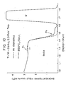
- Fig. 8 is a graph showing the relationship between the barrier height ⁇ B and the annealing temperature, the ordinate representing the barrier height ⁇ B (V) and the abscissa the annealing temperature (°C).
- the solid line shows the characteristics of the Ti/W silicide alloy and the broken line- the characteristics of the Ti/W alloy.
- the barrier height in the case of the Ti/W silicide alloy is more stable against heat-treatment than in the case of the Ti/W alloy.
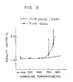
- Fig. 9 is a graph showing the relationship between the ideality factor n if and the annealing temperature, the ordinate representing the ideality factor n if and the abscissa the annealing temperature (°C).
- the solid line indicates the characteristics of the Ti/W silicide alloy and the broken line the characteristics of the Ti/W alloy.
- the ideality factor n if of the Ti/W silicide alloy slightly increases with the annealing temperature but this increase is so negligibly small that the ideality factor n if can be regarded as almost constant as compared with the ideality factor n if of the Ti/W alloy.
- Figs. 10 and 11 are graphs showing the results of examination of reaction between substances through the backscattering method using 4 He with an accelerating energy of 2.0 MeV, the ordinate represents the count of 4 He back scattered and the abscissa the energy of 4 He backscattered.
- Fig. 10 indicates the case of the Ti/W alloy being used, the solid line showing the spectrum obtained in the case where the Ti/W alloy deposited was held as it was and the broken line the spectrum obtained after annealing in a hydrogen (H 2 ) atmosphere at 850°C for 15 minutes.
- Fig. 11 shows the case of the Ti/W silicide alloy being used. There is no difference in spectrum between the case of the T i/ W silicide alloy deposited being held as it was and the case of the alloy being annealed in a hydrogen (H 2 ) atmosphere at 850°C for an hour.
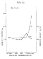
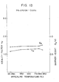
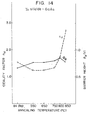
- Figs. 12 to 15 are graphical representations of the data given the above tables.
- the light-hand ordinate represents the ideality factor n if
- the right-hand ordinate the barrier height 0 B and the abscissa the annealing temperature
- the solid line showing the barrier height ⁇ B and the broken line the ideality factor n if .
- Fig. 12 shows the case of molybdenum
- Fig. 13 the case of MoSi
- Fig. 14 the case of T aSi and F ig. 15 the case of WSi.
- tantalum and tungsten no data are obtainable as explained above, and hence graphical showings are meaningless.
- the Schottky contact is retained between the ion-implanted region and a semiconductor layer.
- Fig. 16 is a perspective view showing a model used for obtaining the abovesaid data.
- reference numeral 11 indicates a GaAs substrate having a carrier concentration of about 2x10 17 cm ; 12 designates a Schottky gate electrode measuring 100x150 ⁇ m and 2000 A thick; and 13 identifies an electrode formed of AuGe/Au, the thicknesses of the AuGe and ° Au layers being 200 A and 2000 A, respectively.
- the electrode 13 was heat-treated at 450°C for 2 minutes.
- the I-V characteristic is measured applying a voltage across the electrodes 12 and 13.
- the present invention by using the refractory metal silicide for the Schottky gate electrode, positioning of source and drain regions can be effected by self alignment relative to the gate electrode. Accordingly, the present invention permits miniaturization of semiconductor devices employing the Schottky gate electrode, and hence it is of great utility when employed for fabrication of a semiconductor integrated circuit using a plurality of such semiconductor devices. Furthermore, the gate electrode structure according to the present invention can also be employed as a gate electrode of a high electron mobility transistor (HEMT).
- HEMT high electron mobility transistor
- the composition of the alloyed film is not limited specifically to a stoichiometric alloy composition but may also be different from its stoichiometric value.
Landscapes
- Junction Field-Effect Transistors (AREA)
- Electrodes Of Semiconductors (AREA)
Applications Claiming Priority (2)
| Application Number | Priority Date | Filing Date | Title |
|---|---|---|---|
| JP55189544A JPS57113289A (en) | 1980-12-30 | 1980-12-30 | Semiconductor device and its manufacture |
| JP189544/80 | 1980-12-30 |
Publications (2)
| Publication Number | Publication Date |
|---|---|
| EP0055932A1 true EP0055932A1 (fr) | 1982-07-14 |
| EP0055932B1 EP0055932B1 (fr) | 1985-09-11 |
Family
ID=16243081
Family Applications (1)
| Application Number | Title | Priority Date | Filing Date |
|---|---|---|---|
| EP81306151A Expired EP0055932B1 (fr) | 1980-12-30 | 1981-12-24 | Electrode de grille Schottky pour dispositif à semiconducteur composé et son procédé de fabrication |
Country Status (4)
| Country | Link |
|---|---|
| US (1) | US4566021A (fr) |
| EP (1) | EP0055932B1 (fr) |
| JP (1) | JPS57113289A (fr) |
| DE (1) | DE3172279D1 (fr) |
Cited By (1)
| Publication number | Priority date | Publication date | Assignee | Title |
|---|---|---|---|---|
| FR2571548A1 (fr) * | 1984-10-09 | 1986-04-11 | Thomson Csf | Dispositif semiconducteur comportant un contact schottky, et procede de realisation d'un tel dispositif |
Families Citing this family (23)
| Publication number | Priority date | Publication date | Assignee | Title |
|---|---|---|---|---|
| US5536967A (en) * | 1980-12-30 | 1996-07-16 | Fujitsu Limited | Semiconductor device including Schottky gate of silicide and method for the manufacture of the same |
| JPS59141272A (ja) * | 1983-02-02 | 1984-08-13 | Matsushita Electric Ind Co Ltd | 半導体装置の製造方法 |
| JPS6012776A (ja) * | 1983-03-15 | 1985-01-23 | アイテイ−テイ−・インダストリ−ズ・インコ−ポレ−テツド | 半導体装置 |
| JPS6081861A (ja) * | 1983-10-11 | 1985-05-09 | Matsushita Electric Ind Co Ltd | シヨツトキ−障壁半導体装置 |
| JPS6088477A (ja) * | 1983-10-21 | 1985-05-18 | Nec Corp | 半導体装置の製造方法 |
| US5273918A (en) * | 1984-01-26 | 1993-12-28 | Temic Telefunken Microelectronic Gmbh | Process for the manufacture of a junction field effect transistor |
| JPS61108174A (ja) * | 1984-11-01 | 1986-05-26 | Matsushita Electric Ind Co Ltd | 電界効果トランジスタの製造方法 |
| JPS61206243A (ja) * | 1985-03-08 | 1986-09-12 | Mitsubishi Electric Corp | 高融点金属電極・配線膜を用いた半導体装置 |
| EP0206274B1 (fr) * | 1985-06-21 | 1991-10-23 | Honeywell Inc. | Structure IC complémentaire à haute transconductance |
| US5140387A (en) * | 1985-11-08 | 1992-08-18 | Lockheed Missiles & Space Company, Inc. | Semiconductor device in which gate region is precisely aligned with source and drain regions |
| JPS6346779A (ja) * | 1986-08-15 | 1988-02-27 | Nec Corp | 半導体装置 |
| JPH01120818A (ja) * | 1987-09-23 | 1989-05-12 | Siemens Ag | 低伝達抵抗オーム接触の形成方法 |
| KR930007440B1 (ko) * | 1989-02-02 | 1993-08-10 | 마쓰시다 덴끼 산고오 가부시기가이샤 | 고융점 금속 규소화물 박막을 가진 반도체 장치의 제조 방법 |
| JPH0249436A (ja) * | 1989-03-18 | 1990-02-19 | Fujitsu Ltd | 半導体装置の製造方法 |
| JPH063814B2 (ja) * | 1989-03-18 | 1994-01-12 | 富士通株式会社 | 半導体装置の製造方法 |
| JPH0249437A (ja) * | 1989-03-18 | 1990-02-19 | Fujitsu Ltd | 半導体装置の製造方法 |
| JPH0249438A (ja) * | 1989-03-18 | 1990-02-19 | Fujitsu Ltd | 半導体装置の製造方法 |
| US7084423B2 (en) | 2002-08-12 | 2006-08-01 | Acorn Technologies, Inc. | Method for depinning the Fermi level of a semiconductor at an electrical junction and devices incorporating such junctions |
| US6833556B2 (en) | 2002-08-12 | 2004-12-21 | Acorn Technologies, Inc. | Insulated gate field effect transistor having passivated schottky barriers to the channel |
| JP5171232B2 (ja) | 2006-12-15 | 2013-03-27 | 株式会社半導体エネルギー研究所 | 半導体装置の作製方法 |
| US10038063B2 (en) | 2014-06-10 | 2018-07-31 | International Business Machines Corporation | Tunable breakdown voltage RF FET devices |
| US9620611B1 (en) | 2016-06-17 | 2017-04-11 | Acorn Technology, Inc. | MIS contact structure with metal oxide conductor |
| WO2018094205A1 (fr) | 2016-11-18 | 2018-05-24 | Acorn Technologies, Inc. | Transistor à nanofils à source et drain induits par des contacts électriques avec une hauteur de barrière de schottky négative |
Citations (1)
| Publication number | Priority date | Publication date | Assignee | Title |
|---|---|---|---|---|
| GB2040564A (en) * | 1979-01-08 | 1980-08-28 | American Micro Syst | Method of fabricating MOSFETs |
Family Cites Families (6)
| Publication number | Priority date | Publication date | Assignee | Title |
|---|---|---|---|---|
| FR1570259A (fr) * | 1967-07-01 | 1969-06-06 | ||
| IT973289B (it) * | 1972-03-30 | 1974-06-10 | Bosch Gmbh Robert | Procedimento per la registrazione di informazioni e dispositivo cir cuitale per l esecuzione del proce dimento |
| JPS5226042B2 (fr) * | 1973-05-28 | 1977-07-12 | ||
| US4263605A (en) * | 1979-01-04 | 1981-04-21 | The United States Of America As Represented By The Secretary Of The Navy | Ion-implanted, improved ohmic contacts for GaAs semiconductor devices |
| JPS55108763A (en) * | 1979-01-24 | 1980-08-21 | Toshiba Corp | Schottky barrier compound semiconductor device |
| JPS56140667A (en) * | 1980-04-04 | 1981-11-04 | Nec Corp | Semiconductor device |
-
1980
- 1980-12-30 JP JP55189544A patent/JPS57113289A/ja active Granted
-
1981
- 1981-12-24 EP EP81306151A patent/EP0055932B1/fr not_active Expired
- 1981-12-24 DE DE8181306151T patent/DE3172279D1/de not_active Expired
-
1985
- 1985-04-10 US US06/721,144 patent/US4566021A/en not_active Expired - Lifetime
Patent Citations (1)
| Publication number | Priority date | Publication date | Assignee | Title |
|---|---|---|---|---|
| GB2040564A (en) * | 1979-01-08 | 1980-08-28 | American Micro Syst | Method of fabricating MOSFETs |
Non-Patent Citations (3)
| Title |
|---|
| IBM Technical Disclosure Bulletin Vol. 22, No. 10, March 1980 New York L. BERENBAUM et al. "Metal Silicides for Schottky Barrier Diode Applications" pages 4521 to 4522 * |
| International Journal of Electronics Vol. 48, No. 6, June 1980 Basingstoke P.M. BATEV et al. "Schottky Barrier at a Mo-GaAs Contact" pages 511 to 517 * |
| Journal of the Electrochemical Society Vol. 127, No. 2, February 1980 Princeton F. MOHAMMADI et al. "Properties of Sputtered Tungsten Silicide for MOS Integrated Circuit Applications" pages 450 to 454 * page 450, first paragraph to page 451, third paragraph * * |
Cited By (2)
| Publication number | Priority date | Publication date | Assignee | Title |
|---|---|---|---|---|
| FR2571548A1 (fr) * | 1984-10-09 | 1986-04-11 | Thomson Csf | Dispositif semiconducteur comportant un contact schottky, et procede de realisation d'un tel dispositif |
| EP0181246A1 (fr) * | 1984-10-09 | 1986-05-14 | Thomson-Csf | Dispositif semiconducteur comportant un contact Schottky, et procédé de réalisation d'un tel dispositif |
Also Published As
| Publication number | Publication date |
|---|---|
| DE3172279D1 (en) | 1985-10-17 |
| EP0055932B1 (fr) | 1985-09-11 |
| JPS57113289A (en) | 1982-07-14 |
| US4566021A (en) | 1986-01-21 |
| JPH0219975B2 (fr) | 1990-05-07 |
Similar Documents
| Publication | Publication Date | Title |
|---|---|---|
| EP0055932B1 (fr) | Electrode de grille Schottky pour dispositif à semiconducteur composé et son procédé de fabrication | |
| KR920002090B1 (ko) | 전계효과 트랜지스터의 제조방법 | |
| US4232327A (en) | Extended drain self-aligned silicon gate MOSFET | |
| US4343082A (en) | Method of making contact electrodes to silicon gate, and source and drain regions, of a semiconductor device | |
| US4713358A (en) | Method of fabricating recessed gate static induction transistors | |
| JP3184320B2 (ja) | ダイヤモンド電界効果トランジスタ | |
| EP0168125A1 (fr) | Couches de câblage dans des dispositifs semi-conducteurs | |
| US4735913A (en) | Self-aligned fabrication process for GaAs MESFET devices | |
| US4318216A (en) | Extended drain self-aligned silicon gate MOSFET | |
| US4107835A (en) | Fabrication of semiconductive devices | |
| US3660735A (en) | Complementary metal insulator silicon transistor pairs | |
| US4577396A (en) | Method of forming electrical contact to a semiconductor substrate via a metallic silicide or silicon alloy layer formed in the substrate | |
| US4156879A (en) | Passivated V-gate GaAs field-effect transistor | |
| JPH05102072A (ja) | ケイ化物層からなる半導体デバイスおよびそのデバイスの製造方法 | |
| US5882961A (en) | Method of manufacturing semiconductor device with reduced charge trapping | |
| US5536967A (en) | Semiconductor device including Schottky gate of silicide and method for the manufacture of the same | |
| USRE32613E (en) | Method of making contact electrodes to silicon gate, and source and drain regions, of a semiconductor device | |
| US5200349A (en) | Semiconductor device including schotky gate of silicide and method for the manufacture of the same | |
| US4905061A (en) | Schottky gate field effect transistor | |
| US20020102800A1 (en) | Method for the manufacture of a semiconductor device with a field-effect transistor | |
| JPH0235462B2 (fr) | ||
| US4701422A (en) | Method of adjusting threshold voltage subsequent to fabrication of transistor | |
| JPS5837967A (ja) | Mis型半導体装置の製造方法 | |
| EP0057605B1 (fr) | Transistor à effet de champ à grille Schottky et son procédé de fabrication | |
| US4536223A (en) | Method of lowering contact resistance of implanted contact regions |
Legal Events
| Date | Code | Title | Description |
|---|---|---|---|
| PUAI | Public reference made under article 153(3) epc to a published international application that has entered the european phase |
Free format text: ORIGINAL CODE: 0009012 |
|
| AK | Designated contracting states |
Designated state(s): DE FR GB NL |
|
| 17P | Request for examination filed |
Effective date: 19830105 |
|
| GRAA | (expected) grant |
Free format text: ORIGINAL CODE: 0009210 |
|
| AK | Designated contracting states |
Designated state(s): DE FR GB NL |
|
| REF | Corresponds to: |
Ref document number: 3172279 Country of ref document: DE Date of ref document: 19851017 |
|
| ET | Fr: translation filed | ||
| PLBE | No opposition filed within time limit |
Free format text: ORIGINAL CODE: 0009261 |
|
| STAA | Information on the status of an ep patent application or granted ep patent |
Free format text: STATUS: NO OPPOSITION FILED WITHIN TIME LIMIT |
|
| 26N | No opposition filed | ||
| PGFP | Annual fee paid to national office [announced via postgrant information from national office to epo] |
Ref country code: FR Payment date: 20001212 Year of fee payment: 20 |
|
| PGFP | Annual fee paid to national office [announced via postgrant information from national office to epo] |
Ref country code: DE Payment date: 20001218 Year of fee payment: 20 |
|
| PGFP | Annual fee paid to national office [announced via postgrant information from national office to epo] |
Ref country code: GB Payment date: 20001220 Year of fee payment: 20 |
|
| PGFP | Annual fee paid to national office [announced via postgrant information from national office to epo] |
Ref country code: NL Payment date: 20001231 Year of fee payment: 20 |
|
| PG25 | Lapsed in a contracting state [announced via postgrant information from national office to epo] |
Ref country code: GB Free format text: LAPSE BECAUSE OF EXPIRATION OF PROTECTION Effective date: 20011223 |
|
| PG25 | Lapsed in a contracting state [announced via postgrant information from national office to epo] |
Ref country code: NL Free format text: LAPSE BECAUSE OF EXPIRATION OF PROTECTION Effective date: 20011224 |
|
| REG | Reference to a national code |
Ref country code: GB Ref legal event code: PE20 Effective date: 20011223 |
|
| NLV7 | Nl: ceased due to reaching the maximum lifetime of a patent |
Effective date: 20011224 |