EP0055982A2 - Procédé et appareillage pour revêtir des matériaux semi-conducteurs - Google Patents
Procédé et appareillage pour revêtir des matériaux semi-conducteurs Download PDFInfo
- Publication number
- EP0055982A2 EP0055982A2 EP82100011A EP82100011A EP0055982A2 EP 0055982 A2 EP0055982 A2 EP 0055982A2 EP 82100011 A EP82100011 A EP 82100011A EP 82100011 A EP82100011 A EP 82100011A EP 0055982 A2 EP0055982 A2 EP 0055982A2
- Authority
- EP
- European Patent Office
- Prior art keywords
- applicator
- current
- coating
- support means
- potential
- Prior art date
- Legal status (The legal status is an assumption and is not a legal conclusion. Google has not performed a legal analysis and makes no representation as to the accuracy of the status listed.)
- Granted
Links
Images

Classifications
-
- G—PHYSICS
- G03—PHOTOGRAPHY; CINEMATOGRAPHY; ANALOGOUS TECHNIQUES USING WAVES OTHER THAN OPTICAL WAVES; ELECTROGRAPHY; HOLOGRAPHY
- G03C—PHOTOSENSITIVE MATERIALS FOR PHOTOGRAPHIC PURPOSES; PHOTOGRAPHIC PROCESSES, e.g. CINE, X-RAY, COLOUR, STEREO-PHOTOGRAPHIC PROCESSES; AUXILIARY PROCESSES IN PHOTOGRAPHY
- G03C1/00—Photosensitive materials
- G03C1/74—Applying photosensitive compositions to the base; Drying processes therefor
-
- B—PERFORMING OPERATIONS; TRANSPORTING
- B05—SPRAYING OR ATOMISING IN GENERAL; APPLYING FLUENT MATERIALS TO SURFACES, IN GENERAL
- B05D—PROCESSES FOR APPLYING FLUENT MATERIALS TO SURFACES, IN GENERAL
- B05D3/00—Pretreatment of surfaces to which liquids or other fluent materials are to be applied; After-treatment of applied coatings, e.g. intermediate treating of an applied coating preparatory to subsequent applications of liquids or other fluent materials
- B05D3/14—Pretreatment of surfaces to which liquids or other fluent materials are to be applied; After-treatment of applied coatings, e.g. intermediate treating of an applied coating preparatory to subsequent applications of liquids or other fluent materials by electrical means
-
- G—PHYSICS
- G03—PHOTOGRAPHY; CINEMATOGRAPHY; ANALOGOUS TECHNIQUES USING WAVES OTHER THAN OPTICAL WAVES; ELECTROGRAPHY; HOLOGRAPHY
- G03C—PHOTOSENSITIVE MATERIALS FOR PHOTOGRAPHIC PURPOSES; PHOTOGRAPHIC PROCESSES, e.g. CINE, X-RAY, COLOUR, STEREO-PHOTOGRAPHIC PROCESSES; AUXILIARY PROCESSES IN PHOTOGRAPHY
- G03C1/00—Photosensitive materials
- G03C1/76—Photosensitive materials characterised by the base or auxiliary layers
- G03C1/91—Photosensitive materials characterised by the base or auxiliary layers characterised by subbing layers or subbing means
- G03C1/915—Photosensitive materials characterised by the base or auxiliary layers characterised by subbing layers or subbing means using mechanical or physical means therefor, e.g. corona
Definitions
- the present invention relates to means for coating semiconductive materials with electrostatically assisted coating apparatus, in general, and to such apparatus for coating a moving web of such materials, in 'particular.
- a nonuniform thickness coating applied to a moving web of said material will require considerably more drying time for drying the thicker portions of a nonuniform coating than will be required for drying the thinner portions of said nonuniform coating.
- a temperature gradient that is optimum for drying said thicker coating portions is often excessive for optimum drying of said thinner coating portions. Drying time is usually the major factor limiting maximum production rates of many coated products.
- many properties of photographic film, for example, such as sensitivity to light, color saturation, etc. can be adversely affected when constructed with nonuniformly coated sheet materials.
- One of the most effective coating thickness control apparatus in present day use in the coating industry utilizes electrostatics to uniformly deposit coating materials on products to be coated.
- a web or sheet of material to be coated is passed between en electrically conductive support or backing roller and a coating applicator from which coating material flows onto a surface of said web.
- An electrostatic field is established across the gap between the coating applicator and the backing roller by a high voltage power supply whose output terminals are normally connected between said applicator and said roller.
- the electrostatic field causes a coating, of uniform thickness, to be deposited on the web surface to be coated, and permits larger coating gaps to be employed between said coating applicator and the material to be coated. While the voltage magnitude established between said applicator and said roller is less than that required to generate corona, said magnitude often exceeds 3KV DC.
- electrostatically assisted coating apparatus employing voltages in the vicinity of 3KV or more is relatively effective when coating dielectric materials or materials that have a relatively high electrical resistance.
- electrostatically assisted coating apparatus employing voltages in the vicinity of 3KV or more
- excessive heat-generating current levels could result because of the lower electrical resistance of such materials, and this excessive heat would have a detrimental effect on the quality of such materials.
- the greater the conductivity of the semiconductive materials the greater the magnitude of harmful heat-producing current that would be generated for any given level of electrostatic assist.
- a method and device that will coat semiconductive materials with electrostatically assisted coating apparatus at higher electrostatic assist potentials without producing heat-generating current levels that could damage such materials. Excessive heat levels are precluded and higher coating gap potential can be achieved when electrostatically assisted coating apparatus is employed to coat semiconductive materials, by passing an auxiliary current through said semiconductive materials during the coating process in the same region and in a direction opposite . to that of the current produced by the electrostatically assisted coating apparatus such that the difference between the said current produced by said electrostatically assisted coating apparatus and the said auxiliary current is less than or equal to a predetermined value.
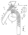
- FIG. 1 generally indicates web coating apparatus employing electrostatic coating-gap assist apparatus constructed in accordance with the teachings of the prior art.
- web support or backing roller 12 is cylindrically shaped, is electrically conductive and is mounted for rotation about backing roller axis 14.
- Coating applicator 16 is mounted in a fixed position with respect to backing roller 12 and is spaced from said roller 12 by distance or gap 18.
- High voltage supply 20 having a DC voltage across its output terminals that is often in the neighborhood of several thousand volts, has said output terminals connected between backing roller 12 and applicator 16 through paths 22 and 24, respectively. Because the coating fluid applied by-applicator 16 maintains said applicator 16 at or near ground potential through a conduit (not shown) supplying coating fluid to-said applicator 16, the high voltage terminal of power supply.20 is connected to said roller 12 and the low voltage terminal of said supply 20 is connected to said grounded applicator 16.
- electrostatic field 26 is produced in coating gap 18 between high potential backing roller 12 and grounded applicator 16.
- insulative or dielectric web material 28 is moved in direction 30 through gap 18 by drive means (not shown), said web 28 is electrostatically charged by orienting its dipoles (such as dipoles 31) by means of said electrostatic field 26.
- the electrostatic charge produced on web 28 by electrostatic field 26 causes fluid 32 following from applicator 16 into coating gap 18 to be attracted toward and uniformly deposited on said moving web 28.
- coating material 32 An extremely important factor in the web coating process is the maintenance of a proper amount of coating material 32 in gap 18 for proper web-coating purposes.
- This portion of coating material 32 is sometimes referred to as a coating fluid bead and is designated numeral 34 in prior art Fig. 1.
- the surface of web 28 that is to be coated moves faster than the rate at which coating fluid 32 moves onto said web 28 surface.
- the faster moving web 28 pulls and thereby stretches said fluid 32 causing the thickness of coating fluid 32 to be reduced to a desired level-
- the electrostatic field 26 changes properties of coating fluid 32 such surface tension allowing fluid 32 to be stretched to a greater degree and over a larger gap between web 28 and applicator 16 without losing or breaking bead 34 than would be possible if electrostatic gap-assisting field 26 were not present.
- gap 18 in Fig. 1 must be large enough to accommodate such things as web splices or foreign matter so that said splices or matter do not come into contact with applicator 16 and thereby adversely affect web coating thickness and/or surface quality.
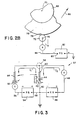
- FIG. 2A schematically depicts electrical circuit analog 37 of the electrostatic coating-gap assist apparatus that is schematically illustrated in said Fig. 2A.
- web support or backing roller 38 is cylindrically shaped, is electrically conductive and is mounted for rotation about backing roller axis 40.
- Coating applicator 42 is mounted in a fixed position with respect to backing roller 38 and is spaced from said roller 38 by distance or gap 44.
- Primary high voltage supply 46 having a DC voltage across its output terminals that is often in the neighborhood of several thousand volts, has said output terminals connected between backing roller 38 and applicator 42 through paths 48 and 50, respectively.
- the high voltage terminal of power supply 46 is necessarily connected to said roller 38 and the low voltage terminal of said supply 46 is connected to said grounded applicator 42.
- Conductive bristle brush 52 is mounted in a fixed position with respect to and has the free ends of its bristles pointed toward and spaced from said grounded backing roller 38.
- DC power supply 54 has its high voltage output terminal connected to one end of each of the bristles of said conductive bristle brush 52 through path 56 and has its low voltage output terminal connected to applicator 42 through paths 58 and 50.
- Portion 60 of semiconductive web 62 ⁇ is supported in gap 44 in a spaced relation from applicator 42 by web backing roller or support means 38.
- Portion 64 of said web 62 is supported by said backing roller 38 such that outer surface 66 of said web portion 64 is in direct physical contact with the free ends of the conductive bristles of brush 52.
- the function of brush 52 is to provide a moving or sliding electrical contact between surface 66 of web-portion 64 and the high voltage output terminal of auxiliary power supply 54 through path 56 and said brush 52.
- Other moving contact arrangements may be substituted for that provided by brush 52.
- One such moving contact arrangement may take the form of that shown in Fig. 2B.
- electrically conductive web support or backing roller 68 of cylindrical shape is mounted for rotation about backing roller axis 70.
- Conductive rubber roller 72 is mounted for rotation about axis 74 and is spaced from web support roller 68.
- a portion of web 76 is supported between rollers 68 and 72 such that one surface of web 76 is in contact with roller 68 and another or the outer surface 78 of web 76 is in contact with conductive rubber roller 72.
- High voltage output terminal 80 of auxiliary DC power supply 82 is connected to surface 78 of web 76 through conductive rubber roller 72 that is connected to said terminal 80 through conductive path 84.
- Another less desirable arrangement may take the form of an electrically conductive path between the high voltage terminal of power supply 54 and backing roller 38 in Fig. 2A that includes a resistor whose resistance value is equivalent to the electrical resistance of portion 64 of semi- conductive web 62 that is presented to said power supply 54.
- An advantage of this arrangement is that said equivalent resistor can be selected such that it-has a larger wattage or heat rating than portion 64 of said web 62.
- auxiliary power supply 54 Current I 1 flows from the low voltage terminal of auxiliary power supply 54 to grounded applicator 42 through conductive paths 58 and 50, across gap 44, through portion 60 of semiconductive web 62 in a direction opposite to current I 2 that is flowing from power supply 46, through conductive support or backing roller 38, through portion 64 of semiconductive web 62 and than back to the high potential side of power supply 54 through the sliding contact provided by brush 52, and electrically conductive path 56.
- the magnitude of current I 1 to be supplied to portion 60 of semiconductive web 62 by auxiliary power supply 54 is primarily though indirectly determined by the conductivity of semiconductive material 62.
- the effective current passing through portion 60 of web 62 should be zero which means current I 1 from auxiliary power supply 54 should be exactly equal in magnitude and opposite in direction to current I 2 flowing from primary power supply 46, a magnitude that is primarily determined by web 62 conductivity.
- the magnitude of current I 1 is empiracally determined by such things as the desired electrical potential level on backing roller 38 and/or 60 of web 62 by differential current I 2 minus I 1 .
- Current I 2 is dependent upon the conductivity of web 62 and the magnitude of current I 1 is adjusted until it approximates current I 2 .
- the heat generated by a differential current (I2-I1) of up to 5ma is acceptable.
- coating fluid 90 from coating applicator 42 is uniformlydepos- ited on semiconductive web 62 with the aid of the assisting forces provided by electrostatic field 88.
- a low electrical impedance in coating gap 44 in the semiconductive material coating apparatus of Fig. 2A will normally cause the potential on backing roller 38 in said Fig. 2A to be maintained at a level that is substantially below that necessary for effective coating-gap assist.
- the electrical impedance of gap 44 is increased thereby enabling higher gap assisting electrical potentials to be employed in, for example, said backing roller 38.
- electrostatic field 88 in coating gap 44 of Fig. 2A and the coating assisting forces produced by said field 88 are primarily dependent upon the voltage across and not the current through said gap 44. Therefore, when auxiliary current I 1 is passed through portion 60 of semiconductive web 62 in a direction opposite to that of primary power supply current I 2 in order to neutralize the effects that would otherwise be produced in web 62 by said current I 2 if .it were not so neutralized by said current I 1 , a desired voltage differential in the vicinity of 3KV DC or more can be maintained across gap'44 in order to generate a coating assisting electrostatic field in said gap 44, and without causing excessive current-related heat to be produced in semiconductive web 62.
- semiconductive material employed herein when describing the preferred embodiment of the present invention encompasses an extremely wide range of material resistances.
- Semiconductive materials are normally considered those that have an electrical resistance greater than that of a pure conductor but less than 1 x 10 10 ohms. However, the actual ohmic value of the material to be coated is not the controlling factor.
- the primary considerations are the desired voltage level across the coating gap and/or the level of heat that would be produced in the semiconductive material for any given level of coating gap voltage. The lower the semiconductive material resistance the higher the magnitude of current-related heat that will be produced without an auxiliary current and the higher must be the magnitude of said auxiliary current to neutralize the effects of such heat.
- Power supplies 46 and 54 have been described above in the preferred embodiment of the present invention as two separate power supplies. However, a single power supply capable of supplying the currents and voltages provided by power supplies 46 and 54 may also be utilized.
- roller 38 and said applicator 42 are sometimes referred to herein as electrodes.
- electrostatic field means one species of electric field.
Landscapes
- Chemical & Material Sciences (AREA)
- Engineering & Computer Science (AREA)
- Materials Engineering (AREA)
- Physics & Mathematics (AREA)
- General Physics & Mathematics (AREA)
- Application Of Or Painting With Fluid Materials (AREA)
- Coating Apparatus (AREA)
- Encapsulation Of And Coatings For Semiconductor Or Solid State Devices (AREA)
Applications Claiming Priority (2)
| Application Number | Priority Date | Filing Date | Title |
|---|---|---|---|
| US06/222,333 US4489672A (en) | 1981-01-05 | 1981-01-05 | Apparatus for coating semiconductive material |
| US222333 | 1998-12-29 |
Publications (3)
| Publication Number | Publication Date |
|---|---|
| EP0055982A2 true EP0055982A2 (fr) | 1982-07-14 |
| EP0055982A3 EP0055982A3 (en) | 1983-02-02 |
| EP0055982B1 EP0055982B1 (fr) | 1986-11-12 |
Family
ID=22831783
Family Applications (1)
| Application Number | Title | Priority Date | Filing Date |
|---|---|---|---|
| EP82100011A Expired EP0055982B1 (fr) | 1981-01-05 | 1982-01-04 | Procédé et appareillage pour revêtir des matériaux semi-conducteurs |
Country Status (5)
| Country | Link |
|---|---|
| US (1) | US4489672A (fr) |
| EP (1) | EP0055982B1 (fr) |
| JP (1) | JPS57184466A (fr) |
| CA (1) | CA1197090A (fr) |
| DE (1) | DE3274199D1 (fr) |
Cited By (1)
| Publication number | Priority date | Publication date | Assignee | Title |
|---|---|---|---|---|
| EP0055983B1 (fr) * | 1981-01-05 | 1987-05-06 | Polaroid Corporation | Aire de revêtement assistée électrostatiquement |
Families Citing this family (7)
| Publication number | Priority date | Publication date | Assignee | Title |
|---|---|---|---|---|
| US5152838A (en) * | 1989-01-17 | 1992-10-06 | Polaroid Corporation | Coating fluid drying apparatus |
| US5609553A (en) * | 1992-11-09 | 1997-03-11 | American Roller Company | Ceramic roller for ESA printing and coating |
| JPH0655051U (ja) * | 1992-12-14 | 1994-07-26 | 石川島播磨重工業株式会社 | 冷水塔 |
| US6146685A (en) * | 1998-11-05 | 2000-11-14 | Delsys Pharmaceutical Corporation | Method of deposition a dry powder and dispensing device |
| US20030136342A1 (en) * | 2000-03-14 | 2003-07-24 | Benjamin Mendez-Gallon | Application device |
| US6368675B1 (en) | 2000-04-06 | 2002-04-09 | 3M Innovative Properties Company | Electrostatically assisted coating method and apparatus with focused electrode field |
| US6475572B2 (en) | 2000-04-06 | 2002-11-05 | 3M Innovative Properties Company | Electrostatically assisted coating method with focused web-borne charges |
Family Cites Families (13)
| Publication number | Priority date | Publication date | Assignee | Title |
|---|---|---|---|---|
| US2052131A (en) * | 1933-10-10 | 1936-08-25 | Us Rubber Co | Spreading, extruding, or like operations |
| US2774921A (en) * | 1953-04-23 | 1956-12-18 | Haloid Co | Apparatus for electrostatically charging insulating image surfaces for electrophotography |
| BE561953A (fr) * | 1956-11-01 | |||
| NL295722A (fr) * | 1962-07-31 | |||
| US3335026A (en) * | 1963-07-16 | 1967-08-08 | Gevaert Photo Prod Nv | Method for coating liquid compositions employing electrostatic field |
| US3484275A (en) * | 1965-05-17 | 1969-12-16 | Scott Paper Co | Electrostatic deposition of compositions on sheet materials utilizing pre-existing friction induced electrostatic charges on said sheet materials |
| JPS497050B1 (fr) * | 1965-12-23 | 1974-02-18 | ||
| US3474292A (en) * | 1966-03-01 | 1969-10-21 | Du Pont | Method of reducing electrostatic charges on film structures |
| US3702258A (en) * | 1969-03-05 | 1972-11-07 | Eastman Kodak Co | Web treatment method |
| US3671806A (en) * | 1970-11-20 | 1972-06-20 | Eastman Kodak Co | Method of and apparatus for applying an electrical charge to a moving sheet of flexible material |
| US3729648A (en) * | 1971-09-30 | 1973-04-24 | Eastman Kodak Co | Method and apparatus for treating a web |
| US4088093A (en) * | 1976-04-13 | 1978-05-09 | Continental Can Company, Inc. | Web coating and powder feed |
| US4402035A (en) * | 1980-09-02 | 1983-08-30 | Polaroid Corporation | Low voltage electrostatic charge regulating apparatus |
-
1981
- 1981-01-05 US US06/222,333 patent/US4489672A/en not_active Expired - Fee Related
-
1982
- 1982-01-04 CA CA000393506A patent/CA1197090A/fr not_active Expired
- 1982-01-04 DE DE8282100011T patent/DE3274199D1/de not_active Expired
- 1982-01-04 EP EP82100011A patent/EP0055982B1/fr not_active Expired
- 1982-01-05 JP JP57000546A patent/JPS57184466A/ja active Granted
Cited By (1)
| Publication number | Priority date | Publication date | Assignee | Title |
|---|---|---|---|---|
| EP0055983B1 (fr) * | 1981-01-05 | 1987-05-06 | Polaroid Corporation | Aire de revêtement assistée électrostatiquement |
Also Published As
| Publication number | Publication date |
|---|---|
| JPH0245335B2 (fr) | 1990-10-09 |
| DE3274199D1 (en) | 1987-01-02 |
| EP0055982B1 (fr) | 1986-11-12 |
| EP0055982A3 (en) | 1983-02-02 |
| JPS57184466A (en) | 1982-11-13 |
| US4489672A (en) | 1984-12-25 |
| CA1197090A (fr) | 1985-11-26 |
Similar Documents
| Publication | Publication Date | Title |
|---|---|---|
| EP0055983B1 (fr) | Aire de revêtement assistée électrostatiquement | |
| US4517143A (en) | Method and apparatus for uniformly charging a moving web | |
| US4826703A (en) | Method and apparatus for electrically controlling coating layer dimensions | |
| US3702258A (en) | Web treatment method | |
| US4513683A (en) | Coating uniformity improvement apparatus | |
| CA1087934A (fr) | Appareil de poudrage en continu et alimentateur en poudre | |
| US2952559A (en) | Method of coating a liquid photographic emulsion on the surface of a support | |
| US3863108A (en) | Electrostatic charge controller | |
| US4486808A (en) | Apparatus for controlling random charges on a moving web | |
| EP1870169B1 (fr) | Systeme de revetement de feuille d'isolation electrique et procede de production de feuille d'isolation electrique recouverte d'un film | |
| US4489672A (en) | Apparatus for coating semiconductive material | |
| US3285167A (en) | Electrostatic printing system with controlled powder feed | |
| US3729648A (en) | Method and apparatus for treating a web | |
| US3462286A (en) | Method of coating webs with photographic emulsions or other liquid compositions utilizing an electric field | |
| US3554161A (en) | Developing apparatus | |
| JPH0561151A (ja) | 塗布方法 | |
| GB1325580A (en) | Method and apparatus for increasing the charge density on the surface of non-conductive materials in industrial processes | |
| US3697303A (en) | Process for coating the surface of a material | |
| US3757163A (en) | Web treatment apparatus and methods | |
| EP0055985B1 (fr) | Technique pour augmenter l'uniformité d'un revêtement | |
| US4825334A (en) | High potential brush polarizer | |
| JP4396084B2 (ja) | 電気絶縁性シートの製造方法 | |
| JPS6229887B2 (fr) | ||
| JP2001046924A (ja) | 静電植毛並に静電塗装を施す静電加工室 | |
| US6242051B1 (en) | Coating method using electrostatic assist |
Legal Events
| Date | Code | Title | Description |
|---|---|---|---|
| PUAI | Public reference made under article 153(3) epc to a published international application that has entered the european phase |
Free format text: ORIGINAL CODE: 0009012 |
|
| AK | Designated contracting states |
Designated state(s): DE FR GB |
|
| PUAL | Search report despatched |
Free format text: ORIGINAL CODE: 0009013 |
|
| AK | Designated contracting states |
Designated state(s): DE FR GB |
|
| 17P | Request for examination filed |
Effective date: 19830909 |
|
| GRAA | (expected) grant |
Free format text: ORIGINAL CODE: 0009210 |
|
| AK | Designated contracting states |
Kind code of ref document: B1 Designated state(s): DE FR GB |
|
| REF | Corresponds to: |
Ref document number: 3274199 Country of ref document: DE Date of ref document: 19870102 |
|
| ET | Fr: translation filed | ||
| PLBE | No opposition filed within time limit |
Free format text: ORIGINAL CODE: 0009261 |
|
| STAA | Information on the status of an ep patent application or granted ep patent |
Free format text: STATUS: NO OPPOSITION FILED WITHIN TIME LIMIT |
|
| 26N | No opposition filed | ||
| PGFP | Annual fee paid to national office [announced via postgrant information from national office to epo] |
Ref country code: FR Payment date: 19901210 Year of fee payment: 10 |
|
| PGFP | Annual fee paid to national office [announced via postgrant information from national office to epo] |
Ref country code: GB Payment date: 19901212 Year of fee payment: 10 |
|
| PGFP | Annual fee paid to national office [announced via postgrant information from national office to epo] |
Ref country code: DE Payment date: 19901231 Year of fee payment: 10 |
|
| PG25 | Lapsed in a contracting state [announced via postgrant information from national office to epo] |
Ref country code: GB Effective date: 19920104 |
|
| GBPC | Gb: european patent ceased through non-payment of renewal fee | ||
| PG25 | Lapsed in a contracting state [announced via postgrant information from national office to epo] |
Ref country code: FR Effective date: 19920930 |
|
| PG25 | Lapsed in a contracting state [announced via postgrant information from national office to epo] |
Ref country code: DE Effective date: 19921001 |
|
| REG | Reference to a national code |
Ref country code: FR Ref legal event code: ST |