EP0056593B1 - Dispositif de commutation pour le réglage de l'alimentation d'un appareil utilisateur - Google Patents
Dispositif de commutation pour le réglage de l'alimentation d'un appareil utilisateur Download PDFInfo
- Publication number
- EP0056593B1 EP0056593B1 EP82100113A EP82100113A EP0056593B1 EP 0056593 B1 EP0056593 B1 EP 0056593B1 EP 82100113 A EP82100113 A EP 82100113A EP 82100113 A EP82100113 A EP 82100113A EP 0056593 B1 EP0056593 B1 EP 0056593B1
- Authority
- EP
- European Patent Office
- Prior art keywords
- transistor
- voltage
- resistor
- transformer
- parallel
- Prior art date
- Legal status (The legal status is an assumption and is not a legal conclusion. Google has not performed a legal analysis and makes no representation as to the accuracy of the status listed.)
- Expired
Links
Images
Classifications
-
- H—ELECTRICITY
- H02—GENERATION; CONVERSION OR DISTRIBUTION OF ELECTRIC POWER
- H02M—APPARATUS FOR CONVERSION BETWEEN AC AND AC, BETWEEN AC AND DC, OR BETWEEN DC AND DC, AND FOR USE WITH MAINS OR SIMILAR POWER SUPPLY SYSTEMS; CONVERSION OF DC OR AC INPUT POWER INTO SURGE OUTPUT POWER; CONTROL OR REGULATION THEREOF
- H02M3/00—Conversion of DC power input into DC power output
- H02M3/22—Conversion of DC power input into DC power output with intermediate conversion into AC
- H02M3/24—Conversion of DC power input into DC power output with intermediate conversion into AC by static converters
- H02M3/28—Conversion of DC power input into DC power output with intermediate conversion into AC by static converters using discharge tubes with control electrode or semiconductor devices with control electrode to produce the intermediate AC
- H02M3/325—Conversion of DC power input into DC power output with intermediate conversion into AC by static converters using discharge tubes with control electrode or semiconductor devices with control electrode to produce the intermediate AC using devices of a triode or a transistor type requiring continuous application of a control signal
- H02M3/335—Conversion of DC power input into DC power output with intermediate conversion into AC by static converters using discharge tubes with control electrode or semiconductor devices with control electrode to produce the intermediate AC using devices of a triode or a transistor type requiring continuous application of a control signal using semiconductor devices only
- H02M3/33507—Conversion of DC power input into DC power output with intermediate conversion into AC by static converters using discharge tubes with control electrode or semiconductor devices with control electrode to produce the intermediate AC using devices of a triode or a transistor type requiring continuous application of a control signal using semiconductor devices only with automatic control of the output voltage or current, e.g. flyback converters
-
- H—ELECTRICITY
- H02—GENERATION; CONVERSION OR DISTRIBUTION OF ELECTRIC POWER
- H02J—ELECTRIC POWER NETWORKS; CIRCUIT ARRANGEMENTS OR SYSTEMS FOR SUPPLYING OR DISTRIBUTING ELECTRIC POWER; SYSTEMS FOR STORING ELECTRIC ENERGY
- H02J7/00—Circuit arrangements for charging or discharging batteries or for supplying loads from batteries
- H02J7/02—Circuit arrangements for charging or discharging batteries or for supplying loads from batteries for charging batteries from AC mains by converters
-
- H—ELECTRICITY
- H02—GENERATION; CONVERSION OR DISTRIBUTION OF ELECTRIC POWER
- H02J—ELECTRIC POWER NETWORKS; CIRCUIT ARRANGEMENTS OR SYSTEMS FOR SUPPLYING OR DISTRIBUTING ELECTRIC POWER; SYSTEMS FOR STORING ELECTRIC ENERGY
- H02J2207/00—Details of circuit arrangements for charging or discharging batteries or supplying loads from batteries
- H02J2207/20—Charging or discharging characterised by the power electronics converter
Definitions
- the invention relates to a circuit arrangement for the controlled supply of a consumer consisting of an accumulator and a DC motor from a DC voltage source of different voltage.
- a voltage transformation which can be carried out capacitively or inductively, is required to adapt the small devices or accumulators to the different voltages.
- a transistor converter circuit is already known, with the aid of which a charging current for an accumulator and, on the other hand, a higher direct current for driving a motor can be generated from an AC mains voltage (DE-OS 2 014 377, US Pat. No. 3,568,038 ).
- a high-frequency flow converter with a saturable core is provided, which is connected to the rectified mains voltage on the primary side and supplies the desired currents on the secondary side.
- the known circuit can only be operated at a certain mains voltage, so it does not automatically adapt to different voltages. Since the core of the converter saturates, the efficiency is low and thermal problems arise.
- a transistor converter circuit in which the primary winding of a transformer is connected in series with the switching path of a first transistor and a DC voltage source.
- the base of the transistor is connected both to a connection of the secondary winding of the transformer and to a switching path connection of a second transistor.
- the base of the second transistor is connected via a Zener diode to the smoothed output voltage, which is tapped via a diode from the other winding connection of the secondary winding of the transformer.
- a tap of the secondary winding of the transformer is connected to a voltage divider with a first and a second resistor, with which a diode is connected in series.
- the oscillation of the transistor converter is initiated in that a small current flows through the first resistor of the voltage divider and via the tap of the secondary winding of the transformer into the base of the most transistor.
- the switching-on process of the first transistor is supported by the positive feedback coupling of the transistor, so that the collector current of the first transistor increases until the base current falls as a result of the saturation of the transformer and the first transistor switches off due to the positive feedback coupling.
- the first transistor is switched on, the energy stored in the transformer flows via the secondary diode into an output capacitor If the current flowing into the output capacitor drops to zero, the current flow in the windings of the transformer breaks down and the switching-on process of the first transistor is initiated again .
- the known transistor converter is however not suitable for charging a rechargeable battery in a stabilized charging current or for operating a DC motor with constant operation; Voltage for the DC motor when operating on DC voltage sources with very different voltage levels.
- a flyback converter for constant voltage supply of in particular integrated circuits or microcomputers b 4 is known, which is optionally available with an alternating voltage of 110 V or 220 V can be operated.
- the blocking converter has in series with the primary winding of a transformer the switching path of a first trai sistor and an emitter resistor.
- a second transistor is connected on the collector side to the base of the first transistor and is connected to the emitter resistor with its E base. Via a winding, a diode and a photo transistor, which is part of an optocoupler, the base of the second transistor is additionally proportional to the input voltage Control signal applied.
- the photodiode of the 0 1 tokopplers is also connected via a Zene diode to the smoothed output voltage of the flyback converter.
- This known arrangement serves to provide multiple, kol possible stante different output voltages E voltage level available.
- a DC voltage converter which contains a Sperrwandl E with a transformer, the switching path ad d frequency of the flyback converter determine the switching path of the primary winding, the transistor is switched.
- a transistor controlling the output voltage is provided, the base of which is connected via a Zenerdioc to the smoothed output voltage of the barrier converter is connected.
- a connection is additionally provided between the base of the transistor determining the oscillation frequency of the flyback converter via a resistor to the smoothed output voltage.
- the known circuit arrangement is intended and suitable exclusively for delivering a constant output voltage with variable input voltages.
- the object of the present invention is to provide a circuit arrangement for the controlled supply of a consumer consisting of a rechargeable battery and a direct current motor from input voltage sources of different voltages using a flyback converter, which stabilizes the charging current during charging operation of the rechargeable battery and a constant operating voltage for the operation of the direct current motor DC motor guaranteed.
- this object is achieved by combining the features a) to g) of claim 1.
- the solution according to the invention ensures during charging that the charging current in the accumulator is stabilized, while a constant operating voltage for the DC motor is ensured when the DC motor is operated from the supply voltage source.
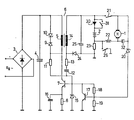
- the circuit arrangement shown in the drawing makes it possible either to charge an accumulator 2 at different input voltages U N or to operate a DC motor 1 which can be connected in parallel.
- One in a wide range of e.g. B. 110 volts to 240 volts changeable AC mains voltage U is fed via a rectifier bridge circuit 3 to the DC voltage terminals of the rectifier bridge circuit 3 input capacitor 4 connected in parallel, both the one DC voltage connection of the rectifier bridge circuit 3 and the one connection of the Input capacitor 4 is connected to ground.
- the series connection of a primary winding 5 of a transformer 6 with the collector-emitter path of a switching transistor 7 is connected in parallel with the DC voltage terminals of the rectifier bridge circuit 3 and the input capacitor 4, the emitter of the switching transistor 7 being connected to ground via a first resistor 8.
- a diode 9 and a third zener diode 10 are provided with opposite polarity in the forward direction.
- the anode of the diode 9 is connected both to the primary winding 5 of the transformer 6 and to a third resistor 11, which is connected to the secondary winding 14 of the transformer 6 via a second capacitor 12 and a fourth resistor 13.
- a second zener diode 15 is additionally connected to the second capacitor 12 and the third resistor 11, which lies parallel to the base-emitter path of the switching transistor 7 and is connected to ground on the anode side.
- the emitter of the switching transistor 7 is also grounded via a fourth capacitor 16.
- the emitter of the control transistor 17 is also connected to ground potential.
- the base of the control transistor 17 is also connected to the anode of a first Zener diode 20, the cathode of which is connected directly to one connection of the DC motor 1 and via a first capacitor 32 to the other connection of the DC motor 1.
- a light-emitting diode 30 In series with the rechargeable battery 2 and the second resistor 23 there is a light-emitting diode 30 with a cathode-side connection to the rechargeable battery 2 and an anode-side connection to the other connection terminal of the secondary winding 14 of the transformer 6 as the charge control lamp.
- This light-emitting diode 30 can be short-circuited by means of a third switch 31 connected in parallel.
- a first switch 21 is provided between the first connection of the DC motor 1 and the accumulator 2, while the second connection of the DC motor 1 is connected via a choke 22 to the connection of the accumulator 2 to the second resistor 23.
- a second switch 26 is provided in parallel with the second resistor 23, with which the choke coil 22 can be connected to ground with its end connected to the accumulator 2.
- the operating state in which the switches 21 and 26 are closed must be distinguished from the operating state in which the switches 21 and 26 are open.
- the DC motor 1 is operated with a constant voltage from the supplying AC voltage network, while in the open state the battery 2 is charged with a stabilized charging current from the supplying AC voltage network.
- the circuit arrangement with closed switches 21 and 26 should be considered. If a variable mains alternating voltage U N is applied to the rectifier bridge circuit 3, the rectified voltage is supplied to the parallel-connected input capacitor 4 via the DC voltage terminals of the rectifier bridge circuit 3. The second capacitor 12 is then charged via the third resistor 11, as a result of which the voltage at the base of the switching transistor 7 rises until it becomes conductive. Since the primary winding 5 of the transformer 6 represents an inductance, the current through the switching transistor 7 increases linearly when the switching transistor 7 is conductive. This current causes a corresponding voltage drop across the first resistor 8.
- the second zener diode 15 connected to the base of the switching transistor 7 and connected to ground on the anode side becomes conductive when the sum of the voltage drop caused by the primary current at the first resistor 8 and the base-emitter voltage of the switching transistor 7 becomes the zener voltage of the second zener diode 15 has reached. Once the breakdown voltage of the second zener diode 15 has been reached, the current through the transistor cannot increase further. The switching transistor 7 is switched off while the voltage on the secondary winding 14 of the transformer 6 changes its polarity.
- the diode 24 becomes conductive so that it charges the third capacitor 25, as a result of which the energy stored in the transformer 6 is discharged via the diode 24 into the consumer consisting of the parallel connection of the accumulator 2 and the direct current motor 1.
- the light-emitting diode 30 can be displayed whether the battery 2 is being charged. If the accumulator 2 is not charged, the switches 31, 21, 26 are all closed, i.e. the light-emitting diode 30 is short-circuited and does not light up.
Landscapes
- Engineering & Computer Science (AREA)
- Power Engineering (AREA)
- Dc-Dc Converters (AREA)
- Heat-Pump Type And Storage Water Heaters (AREA)
- Supplying Of Containers To The Packaging Station (AREA)
- Beans For Foods Or Fodder (AREA)
Claims (3)
Priority Applications (1)
| Application Number | Priority Date | Filing Date | Title |
|---|---|---|---|
| AT82100113T ATE20292T1 (de) | 1981-01-17 | 1982-01-09 | Schaltungsanordnung zur geregelten speisung eines verbrauchers. |
Applications Claiming Priority (2)
| Application Number | Priority Date | Filing Date | Title |
|---|---|---|---|
| DE3101375 | 1981-01-17 | ||
| DE3101375A DE3101375C2 (de) | 1981-01-17 | 1981-01-17 | Schaltungsanordnung zur geregelten Speisung eines Verbrauchers |
Publications (2)
| Publication Number | Publication Date |
|---|---|
| EP0056593A1 EP0056593A1 (fr) | 1982-07-28 |
| EP0056593B1 true EP0056593B1 (fr) | 1986-06-04 |
Family
ID=6122814
Family Applications (1)
| Application Number | Title | Priority Date | Filing Date |
|---|---|---|---|
| EP82100113A Expired EP0056593B1 (fr) | 1981-01-17 | 1982-01-09 | Dispositif de commutation pour le réglage de l'alimentation d'un appareil utilisateur |
Country Status (5)
| Country | Link |
|---|---|
| US (1) | US4441147A (fr) |
| EP (1) | EP0056593B1 (fr) |
| JP (1) | JPS57139828A (fr) |
| AT (1) | ATE20292T1 (fr) |
| DE (2) | DE3101375C2 (fr) |
Families Citing this family (15)
| Publication number | Priority date | Publication date | Assignee | Title |
|---|---|---|---|---|
| DE3218594A1 (de) * | 1982-05-17 | 1983-12-22 | Braun Ag, 6000 Frankfurt | Elektronisches schaltnetzteil |
| AT387875B (de) * | 1983-03-31 | 1989-03-28 | Schrack Elektronik Ag | Schaltungsanordnung zum betreiben einer last |
| DE3323747A1 (de) * | 1983-07-01 | 1985-01-03 | Braun Ag, 6000 Frankfurt | Elektronisches schaltnetzteil |
| DE3334732A1 (de) * | 1983-09-24 | 1985-04-11 | Braun Ag, 6000 Frankfurt | Elektronisches schaltnetzteil mit einem querdrosselwandler |
| US4682079A (en) * | 1984-10-04 | 1987-07-21 | Hallmark Cards, Inc. | Light string ornament circuitry |
| NL8500154A (nl) * | 1985-01-22 | 1986-08-18 | Koninkl Philips Electronics Nv | Zelf-oscillerende voedingsschakeling. |
| NL8503088A (nl) * | 1985-11-11 | 1987-06-01 | Philips Nv | Voedingsschakeling. |
| DE3545324A1 (de) * | 1985-12-20 | 1987-06-25 | Braun Ag | Elektronisches schaltnetzteil |
| DE3803906A1 (de) * | 1988-02-09 | 1989-08-17 | Braun Ag | Verfahren und schaltungsanordnung zur bestimmung der ladezeit eines akkumulators |
| JP2000184698A (ja) * | 1998-12-09 | 2000-06-30 | Murata Mfg Co Ltd | スイッチング電源 |
| CA2306531C (fr) * | 1999-10-15 | 2011-07-12 | Wayne Ernest Conrad | Methode et appareil de transmission de puissance a un systeme mecanique ou electrique |
| DE10017528A1 (de) * | 2000-04-10 | 2001-10-18 | Mettler Toledo Gmbh | Waage mit dichtender Arretierung |
| CA2306291A1 (fr) | 2000-04-20 | 2001-10-20 | Wayne Ernest Conrad | Technique et appareil pour augmenter la vitesse et reduire la consommation de carburant ¬donc, augmenter l'autonomie (la distance franchissable)| des aeronefs, des navires de surface, des sous-marins, des missiles et des torpilles et/ou pour en modifier la signature acoustique |
| US8120363B2 (en) | 2008-11-24 | 2012-02-21 | Cummins Power Generation Ip, Inc. | Voltage drop compensation for an electric power storage device charging system |
| US10015434B2 (en) * | 2016-04-22 | 2018-07-03 | Shenzhen Skyworth-Rgb Electronic Co., Ltd | Switched-mode power supply for outputting a steady voltage and current and television including the same |
Citations (1)
| Publication number | Priority date | Publication date | Assignee | Title |
|---|---|---|---|---|
| US4048219A (en) * | 1974-04-17 | 1977-09-13 | The United States Of America As Represented By The Secretary Of The Navy | Acetals derived from negatively substituted aldehydes and polynitro- or halonitroethanols |
Family Cites Families (11)
| Publication number | Priority date | Publication date | Assignee | Title |
|---|---|---|---|---|
| US3568038A (en) * | 1969-03-28 | 1971-03-02 | Schick Electric Inc | Transistor inverter circuit |
| US3702961A (en) * | 1971-03-19 | 1972-11-14 | Atomic Energy Commission | Demand regulated dc to dc power supply |
| DE2457664C2 (de) * | 1974-12-06 | 1985-04-04 | Robert Bosch Gmbh, 7000 Stuttgart | Elektrische Schaltungsanordnung zur Erzeugung einer stabilen Ausgangsspannung |
| JPS52114915A (en) * | 1976-03-23 | 1977-09-27 | Ricoh Co Ltd | Dc-dc converter |
| JPS5364745A (en) * | 1976-11-20 | 1978-06-09 | Toko Inc | Switching power supply |
| US4155081A (en) * | 1977-10-25 | 1979-05-15 | Honeywell Inc. | Rechargeable battery backup power source for an ionization smoke detector device |
| DE2948054C3 (de) * | 1979-11-29 | 1988-11-10 | Braun Ag, 6000 Frankfurt | Schaltungsanordnung zur geregelten Speisung eines Verbrauchers |
| EP0030026B2 (fr) * | 1979-11-29 | 1989-01-25 | Klaus Becker | Agencement de circuit pour l'alimentation stabilisée d'un utilisateur |
| DE2949421A1 (de) * | 1979-12-08 | 1981-07-02 | Braun Ag, 6000 Frankfurt | Schaltungsanordnung zum laden einer batterie |
| US4316242A (en) * | 1980-09-04 | 1982-02-16 | General Electric Company | Wide input range, transient-immune regulated flyback switching power supply |
| US4376263A (en) * | 1980-11-06 | 1983-03-08 | Braun Aktiengesellschaft | Battery charging circuit |
-
1981
- 1981-01-17 DE DE3101375A patent/DE3101375C2/de not_active Expired
-
1982
- 1982-01-09 EP EP82100113A patent/EP0056593B1/fr not_active Expired
- 1982-01-09 AT AT82100113T patent/ATE20292T1/de active
- 1982-01-09 DE DE8282100113T patent/DE3271408D1/de not_active Expired
- 1982-01-11 JP JP57001861A patent/JPS57139828A/ja active Pending
- 1982-01-11 US US06/338,745 patent/US4441147A/en not_active Expired - Fee Related
Patent Citations (1)
| Publication number | Priority date | Publication date | Assignee | Title |
|---|---|---|---|---|
| US4048219A (en) * | 1974-04-17 | 1977-09-13 | The United States Of America As Represented By The Secretary Of The Navy | Acetals derived from negatively substituted aldehydes and polynitro- or halonitroethanols |
Also Published As
| Publication number | Publication date |
|---|---|
| JPS57139828A (en) | 1982-08-30 |
| US4441147A (en) | 1984-04-03 |
| ATE20292T1 (de) | 1986-06-15 |
| DE3101375C2 (de) | 1983-03-31 |
| DE3101375A1 (de) | 1982-08-05 |
| EP0056593A1 (fr) | 1982-07-28 |
| DE3271408D1 (en) | 1986-07-10 |
Similar Documents
| Publication | Publication Date | Title |
|---|---|---|
| EP0095072B1 (fr) | Dispositif d'alimentation à commutation électronique | |
| EP0056593B1 (fr) | Dispositif de commutation pour le réglage de l'alimentation d'un appareil utilisateur | |
| DE2827693A1 (de) | Wechselrichter und dessen verwendung in einem batterieladegeraet | |
| DE60024195T2 (de) | Stromversorgungseinheit | |
| EP0226128B2 (fr) | Alimentation à découpage électronique | |
| DE3310678C2 (de) | Schaltung zur Regelung der Ausgangsspannung eines elektronischen Schaltnetzteiles | |
| DE69607145T2 (de) | Stromversorgungsschaltung | |
| DE3630421C2 (fr) | ||
| DE4208911B4 (de) | Spannungsversorgung | |
| EP0057910B2 (fr) | Circuit pour l'alimentation régulée d'un utilisateur | |
| DE69602422T2 (de) | Stromversorgungsschaltung | |
| EP0593518B1 (fr) | Unite electronique d'alimentation en energie fournie par le reseau electrique | |
| EP0030276A1 (fr) | Agencement de circuit pour la charge d'une batterie | |
| DE69706625T2 (de) | Schaltnetzteil mit kompensation für eingangsspannungsänderung | |
| EP0262739B1 (fr) | Convertisseur de courant continu à découpage | |
| DE2402182B2 (de) | Ladegerät für Akkumulatoren | |
| EP0152913B1 (fr) | Circuit pour un convertisseur à récupération | |
| DE3103863C2 (de) | Schaltungsanordnung zur Speisung eines Gleichstromverbrauchers mit konstantem Strom aus Eingangsgleichspannungsquellen unterschiedlicher Spannung | |
| EP0320605B1 (fr) | Alimentation électronique à découpage avec un convertisseur à inductance | |
| DE3311737C2 (de) | Elektronisches Schaltnetzteil | |
| DE3347930A1 (de) | Schaltungsanordnung fuer ein sperrwandler-schaltnetzteil | |
| DE2305971A1 (de) | Verfahren und vorrichtung zur ladung einer elektrischen batterie | |
| DE3616189A1 (de) | Selbstanlaufende speiseeinrichtung, insbesondere fuer eisenbahnfahrzeuge | |
| DE4116434A1 (de) | Sperrwandler mit nur einer primaerseitigen uebertrager-hilfswicklung | |
| DE3300285A1 (de) | Elektronisches schaltnetzteil |
Legal Events
| Date | Code | Title | Description |
|---|---|---|---|
| PUAI | Public reference made under article 153(3) epc to a published international application that has entered the european phase |
Free format text: ORIGINAL CODE: 0009012 |
|
| AK | Designated contracting states |
Designated state(s): AT BE CH DE FR GB IT LU NL SE |
|
| 17P | Request for examination filed |
Effective date: 19820811 |
|
| ITF | It: translation for a ep patent filed | ||
| GRAA | (expected) grant |
Free format text: ORIGINAL CODE: 0009210 |
|
| AK | Designated contracting states |
Kind code of ref document: B1 Designated state(s): AT BE CH DE FR GB IT LI LU NL SE |
|
| REF | Corresponds to: |
Ref document number: 20292 Country of ref document: AT Date of ref document: 19860615 Kind code of ref document: T |
|
| REF | Corresponds to: |
Ref document number: 3271408 Country of ref document: DE Date of ref document: 19860710 |
|
| ET | Fr: translation filed | ||
| PGFP | Annual fee paid to national office [announced via postgrant information from national office to epo] |
Ref country code: AT Payment date: 19861231 Year of fee payment: 6 |
|
| PG25 | Lapsed in a contracting state [announced via postgrant information from national office to epo] |
Ref country code: LU Free format text: LAPSE BECAUSE OF NON-PAYMENT OF DUE FEES Effective date: 19870131 |
|
| PGFP | Annual fee paid to national office [announced via postgrant information from national office to epo] |
Ref country code: NL Payment date: 19870131 Year of fee payment: 6 |
|
| PLBI | Opposition filed |
Free format text: ORIGINAL CODE: 0009260 |
|
| 26 | Opposition filed |
Opponent name: N.V. PHILIPS' GLOEILAMPENFABRIEKEN Effective date: 19870302 |
|
| NLR1 | Nl: opposition has been filed with the epo |
Opponent name: N.V. PHILIPS'GLOEILAMPENFABRIEKEN |
|
| PG25 | Lapsed in a contracting state [announced via postgrant information from national office to epo] |
Ref country code: BE Effective date: 19890131 |
|
| RDAG | Patent revoked |
Free format text: ORIGINAL CODE: 0009271 |
|
| STAA | Information on the status of an ep patent application or granted ep patent |
Free format text: STATUS: PATENT REVOKED |
|
| GBPR | Gb: patent revoked under art. 102 of the ep convention designating the uk as contracting state | ||
| 27W | Patent revoked |
Effective date: 19890210 |
|
| REG | Reference to a national code |
Ref country code: CH Ref legal event code: PL |
|
| BERE | Be: lapsed |
Owner name: BRAUN A.G. Effective date: 19890131 |
|
| NLR2 | Nl: decision of opposition | ||
| EUG | Se: european patent has lapsed |
Ref document number: 82100113.8 |