EP0056839B1 - Convertisseur d'image à l'état solide sensible à rayonnement - Google Patents
Convertisseur d'image à l'état solide sensible à rayonnement Download PDFInfo
- Publication number
- EP0056839B1 EP0056839B1 EP81107644A EP81107644A EP0056839B1 EP 0056839 B1 EP0056839 B1 EP 0056839B1 EP 81107644 A EP81107644 A EP 81107644A EP 81107644 A EP81107644 A EP 81107644A EP 0056839 B1 EP0056839 B1 EP 0056839B1
- Authority
- EP
- European Patent Office
- Prior art keywords
- solid
- state image
- image converter
- fets
- radiation sensitive
- Prior art date
- Legal status (The legal status is an assumption and is not a legal conclusion. Google has not performed a legal analysis and makes no representation as to the accuracy of the status listed.)
- Expired
Links
Images

Classifications
-
- H—ELECTRICITY
- H04—ELECTRIC COMMUNICATION TECHNIQUE
- H04N—PICTORIAL COMMUNICATION, e.g. TELEVISION
- H04N5/00—Details of television systems
- H04N5/30—Transforming light or analogous information into electric information
- H04N5/32—Transforming X-rays
Definitions
- the invention relates to a radiation-sensitive solid-state image converter with a number of FETs, which has a substrate with diffused-in working electrodes, on which an insulating layer is applied, which carries conductive gate electrodes in the area of the working electrodes, which are covered by a radiation-sensitive layer on which a transparent conductive electrode is applied, as well as with switching means for optionally non-destructive reading or deleting the charges of the FET and with a clock generator for connection to a video amplifier.
- Such devices convert optical images into television images. They enable a simple, space-saving and weight-saving construction of a television recording device.
- Such a solid-state image converter which has field-effect transistors (FET) as picture elements.
- FET field-effect transistors
- two zones of the other conductivity type, which form the working electrodes of an FET are diffused into a semiconductor substrate of one conductivity type.
- the gate channel of the FET is between the zones.
- a thin insulating layer is applied over the substrate.
- the insulating layer is covered with a conductive gate electrode.
- This charge on the gate electrode changes the conductivity of the gate channel of the FET. If the working electrodes are connected to a voltage, a current flows which is fed to a video amplifier. If several of these FETs are arranged in a matrix and they are connected to the video amplifier one after the other, a television signal is obtained. Once all the information has been read out, an erase voltage is applied to each of the gate electrodes via erase switches so that the charge can flow off and the FET can be erased. After opening the erase switch, the gate electrodes can be recharged by incidence of light. It turns out to be disadvantageous here that a switch must be provided to delete each FET, so that the structure of the integrated circuit proves to be undesirably complex.
- the invention is based on the object of creating a solid-state image converter of the type mentioned at the outset, which is distinguished by a simple structure and in which the packing density of the radiation-sensitive FET can be increased.
- the object is achieved according to the invention in that the gate electrodes of the FET are connected to ground via a protective diode and to one of the working electrodes of the FET via a further protective diode, and in that the switching means are connected to the transparent electrode.
- This structure and the wiring of the solid-state image converter mean that all FETs are read and deleted simultaneously. Since the individual switching means for deleting the gate electrodes of the FET are eliminated, each picture element takes up little space.
- the field of application can be expanded if the radiation-sensitive layer consists of an X-ray-sensitive semiconductor with an internal photo effect.
- a good efficiency in the conversion of X-ray images is achieved if the X-ray sensitive semiconductor is amorphous selenium.
- Simple control is achieved if the solid-state image converter has a two-dimensional FET matrix.
- the sensitivity particularly in the case of X-rays, can be further increased if a voltage source for generating a high suction voltage can be connected to the transparent electrode during the exposure of the radiation-sensitive FET and if the suction voltage can be changed slightly by switching means for reading and deleting the stored information.
- the semiconductor layer has a multi-part structure. Smaller, easier to manufacture transducers can be used advantageously if the semiconductor layer of the solid-state image transducer consists of several disks.
- the clock generator has a simple construction if a horizontal and a vertical shift register are provided which are driven by the clock generator and if the FET are in series with two switching elements which are driven by the shift registers and connected to the video amplifier are.
- the quality of the television picture at low illuminance levels can be further increased if the solid-state image converter is followed by an image memory in which the pixel information of a recording for a television picture is summed up over several time cycles. It has proven to be expedient if the solid-state image converter is used in an X-ray diagnostic device as a television recording device.
- FIG. 2 shows an X-ray sensitive television recording device which replaces the X-ray image intensifier 4 and the television camera 5 and consists of a layer support 10 in which a silicon wafer 11 with integrated circuit technology is arranged.
- a layer of an X-ray transparent material is applied in front of it, which acts as a conductive electrode 13.
- the x-rays are incident on the solid-state image converter 10 to 13 in the direction of the arrows 14.
- a changeable DC voltage source 15 is connected to the electrode 13 in order to generate the high suction voltage compared to the conventional semiconductor technology.
- the integrated output region of the silicon wafer 11 is connected to a video amplifier 16, which amplifies the electrical output signals of the solid-state image converter 10 to 13.
- the video signals are digitized in a downstream analog-to-digital converter (A / D converter) 17 and read into an image memory 18.
- the output of the image memory 18 is connected to a processing circuit 19, one output of which is fed back to the image memory 18 and the other output of which is connected to a digital-to-analog converter (D / A converter) 20. Its analog output signal is fed to the monitor 7, on which the television picture is displayed.
- the clock generator 8 is connected to the silicon wafer 11 of the solid-state image memory 10 to 13, to the image memory 18 and to the processing circuit 19 and controls the timing of the signal processing.
- the incident X-rays generate a charge image corresponding to the X-ray image in the solid-state image converter 10 to 13. This causes an output signal which is read into the image memory 18 in an amplified manner.
- the charge image in the solid-state image converter 10 to 13 is not deleted, but is scanned several times in order to be able to compensate for low output signals caused by low dose values.
- the output signals are summed in the image memory 18 over a plurality of sampling periods, so that the noise of the electrical components is reduced. After the summation has been completed, the saved image can be read out.
- the digital video signal corresponding to the image is processed in the processing circuit 19.
- imperfections for example missing picture elements, which are caused by defective semiconductor elements, can be eliminated by interpolating the information from neighboring picture elements.
- Differences in sensitivity or background structures can be compensated for by means of an empty image (without a recording object) stored in the processing circuit 19 (without a recording object) which is subtracted from the images stored in the image memory 18, so that the solid-state image converter 10 to 13 is calibrated.
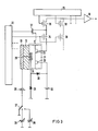
- the mode of operation of the solid-state image converter 10 to 13 is explained in more detail with reference to a semiconductor element in FIG. 3.
- the solid-state image converter 10 to 13 is cut and shown broken off.
- the silicon wafer 11 has a substrate 21 of a conductivity type, into which a drain zone 22 and a source zone 23 are diffused, which are of the opposite conductivity type.
- An insulating layer 24 of a dielectric, for example silicon dioxide, is located on the substrate 21.
- the conductive gate electrode 25 is located in the layer 24 over the space forming the channel of the field effect transistor between the drain zone 22 and the source zone 23.
- the semiconductor layer 12 and the conductive electrode 13 are located on this silicon wafer 11 the variable DC voltage source 15 is connected. It has a voltage source 26, which in this case is shown as the primary element. This voltage source 26 is connected to ground via a changeover switch 27. For reading or erasing, variable voltage sources 28 and 29 are connected in series with voltage source 26.
- the source zone 23 is connected to a voltage source 30, which supplies the operating voltage for this integrated circuit.
- the gate electrode 25 is connected to the cathode of a protective diode 31, the anode of which is connected to ground, and to the anode of a protective diode 32, the cathode of which is connected to the positive pole of the voltage source 30.
- the drain zone 22 is connected to the video amplifier 16 via a field effect transistor 34 controlled by a vertical shift register 33 and via a field effect transistor 36 controlled by a horizontal shift register 35.
- the semiconductor element shown is in the second row of the first column of the matrix.
- the gate electrode of a field effect transistor 37 is connected to a further output of the vertical shift register 33, the drain electrode of which is connected to the source electrode of the field effect transistor 36.
- This field effect transistor 37 switches through the semiconductor element (not shown) in the first column and first line. Further outputs of the vertical shift register 33, shown in broken lines, are provided for driving the field-effect transistors, not shown, which are connected upstream of the remaining semiconductor elements.
- the second output of the horizontal shift register 35 is connected to the gate electrode of a field effect transistor 38, the drain electrode of which is connected to the input of the video amplifier 16.
- the field effect transistor 38 is in series with a field effect transistor 39, the gate electrode of which is connected to the output of the vertical shift register 33 connected to the field effect transistor 34 and the source electrode of which is also connected to a semiconductor element (not shown) which is in the second row and second column.
- the further outputs of the horizontal shift register 35 which are indicated by dashed lines, are provided for driving the field effect transistors assigned to the columns of the matrix.
- Each of the semiconductor elements can thus be connected to the video amplifier 16 by means of two field effect transistors, which are controlled by the shift registers 33 and 35.
- a field effect transistor is assigned to each semiconductor element and is controlled by the vertical shift register 33.
- a further field effect transistor is provided for each column and is controlled by the horizontal shift register 35. This means that for an m x n matrix with m columns and n rows (n + 1) x m field effect transistors are required.
- the output signal of the vertical shift register 33 determines the row of the matrix of the semiconductor elements and the output signal of the horizontal shift register 35 determines the column.
- a suction voltage which can be, for example, ⁇ 2 kV, is applied to the conductive electrode 13 for processing by the voltage source 26. Since the gate electrode 25 is connected to ground via the protective diode 31, a potential difference builds up in the semiconductor layer 12. Then the voltage source 28 is switched on via the changeover switch 27, which has, for example, a voltage of half the operating voltage (5 V) of the integrated circuit. This also increases the potential of the gate electrode 25 to + 5 V. During the exposure, X-rays fall on the semiconductor layer 12, so that its resistance decreases and the gate electrode 25 assumes a more negative potential.
- the information can be read out immediately by switching the semiconductor elements on video amplifier 16 alternately, as already described.
- the switch 27 switches to the voltage source 29, which may have a voltage of + 20 V, for example.
- the potential of the gate electrode 25 is raised and limited to the operating voltage by the protective diode 32, as a result of which the image information is deleted.
- the changeover switch 27 is again brought into the position shown, so that the semiconductor element is prepared for the next exposure.
- This potential switching enables non-destructive reading over several scans.
- a matrix of semiconductor elements it is also possible to use only one row or column which is shifted over the entire receiving area. This reduces the size of the silicon substrate, so that such a solid-state image converter can be manufactured more easily.
- the solid-state image converter 10 to 13 is made up of several, the outlay and the failures during production can be reduced. Since somewhat larger distances must be expected at the joints, the missing pixels can be approximately replaced by the processing circuit.
Landscapes
- Engineering & Computer Science (AREA)
- Multimedia (AREA)
- Signal Processing (AREA)
- Measurement Of Radiation (AREA)
- Transforming Light Signals Into Electric Signals (AREA)
- Solid State Image Pick-Up Elements (AREA)
Claims (10)
Applications Claiming Priority (2)
| Application Number | Priority Date | Filing Date | Title |
|---|---|---|---|
| DE3101504 | 1981-01-19 | ||
| DE19813101504 DE3101504A1 (de) | 1981-01-19 | 1981-01-19 | Roentgendiagnostikeinrichtung mit einer roentgenstrahlenempfindlichen fernsehaufnahmeeinrichtung |
Publications (3)
| Publication Number | Publication Date |
|---|---|
| EP0056839A2 EP0056839A2 (fr) | 1982-08-04 |
| EP0056839A3 EP0056839A3 (en) | 1982-10-27 |
| EP0056839B1 true EP0056839B1 (fr) | 1985-03-13 |
Family
ID=6122878
Family Applications (1)
| Application Number | Title | Priority Date | Filing Date |
|---|---|---|---|
| EP81107644A Expired EP0056839B1 (fr) | 1981-01-19 | 1981-09-25 | Convertisseur d'image à l'état solide sensible à rayonnement |
Country Status (2)
| Country | Link |
|---|---|
| EP (1) | EP0056839B1 (fr) |
| DE (2) | DE3101504A1 (fr) |
Families Citing this family (6)
| Publication number | Priority date | Publication date | Assignee | Title |
|---|---|---|---|---|
| US4689487A (en) * | 1984-09-03 | 1987-08-25 | Kabushiki Kaisha Toshiba | Radiographic image detection apparatus |
| DE3503698A1 (de) * | 1985-02-04 | 1986-08-07 | Siemens AG, 1000 Berlin und 8000 München | Anordnung zum herstellen von roentgenbildern durch computer-radiographie |
| DE3825704A1 (de) * | 1988-07-28 | 1990-02-01 | Siemens Ag | Roentgenstrahlenempfindlicher festkoerperbildwandler |
| DE3901837A1 (de) * | 1989-01-23 | 1990-07-26 | H J Dr Besch | Bildgebender strahlendetektor mit pulsintegration |
| GB2289983B (en) * | 1994-06-01 | 1996-10-16 | Simage Oy | Imaging devices,systems and methods |
| US6035013A (en) * | 1994-06-01 | 2000-03-07 | Simage O.Y. | Radiographic imaging devices, systems and methods |
Family Cites Families (2)
| Publication number | Priority date | Publication date | Assignee | Title |
|---|---|---|---|---|
| JPS5850030B2 (ja) * | 1979-03-08 | 1983-11-08 | 日本放送協会 | 光電変換装置およびそれを用いた固体撮像板 |
| US4245158A (en) * | 1979-03-26 | 1981-01-13 | American Science And Engineering, Inc. | Soft x-ray spectrometric imaging system |
-
1981
- 1981-01-19 DE DE19813101504 patent/DE3101504A1/de not_active Withdrawn
- 1981-09-25 DE DE8181107644T patent/DE3169268D1/de not_active Expired
- 1981-09-25 EP EP81107644A patent/EP0056839B1/fr not_active Expired
Also Published As
| Publication number | Publication date |
|---|---|
| DE3169268D1 (en) | 1985-04-18 |
| EP0056839A3 (en) | 1982-10-27 |
| EP0056839A2 (fr) | 1982-08-04 |
| DE3101504A1 (de) | 1982-08-26 |
Similar Documents
| Publication | Publication Date | Title |
|---|---|---|
| DE69723136T2 (de) | Photoelektrische Wandler-Vorrichtung und photoelektrisches Wandler-System zur Benutzung der Vorrichtung | |
| DE3008858C2 (de) | Fotoelektrische Halbleiteranordnung | |
| DE69635303T2 (de) | Röntgenstrahlungs-bildsensor | |
| DE3531448C2 (fr) | ||
| DE3320661C2 (fr) | ||
| DE69635333T2 (de) | Gerät zur Aufnahme von Röntgenbildern | |
| DE69433993T2 (de) | Photoelektrischer Umwandler, sein Steuerverfahren und System mit diesem photoelektrischen Umwandler | |
| DE69505375T2 (de) | Vorrichtung, system und methoden zur aufnahme von bildern | |
| DE3546212C2 (fr) | ||
| DE69731419T2 (de) | Photoelektrische Umwandlungsvorrichtung und Ansteuermethode dafür | |
| DE69424805T2 (de) | Bildwandlersystem | |
| DE68907017T2 (de) | Photoempfindliche vorrichtung mit signalverstaerkung im bereich der photoempfindlichen punkte. | |
| DE69801059T2 (de) | Vorrichtung zur strahlungsbildaufnahme | |
| DE2912884A1 (de) | Photomessfuehlereinrichtung und diese verwendendes bildabtastsystem | |
| DE3345215C2 (de) | Festkörper-Bildaufnahmewandler | |
| DE3312264A1 (de) | Vorrichtung zur aufnahme von roentgenbildern | |
| DE1289549B (de) | Bildwandlersystem | |
| DE3345176C2 (de) | Festkörper-Bildsensor | |
| EP0004584B1 (fr) | Dispositif pour la mesure de la distance ou de la vitesse d'un objet, utilisation de ce dispositif et procédés d'utilisation | |
| DE69320709T2 (de) | Photoelektrischer Wandler und Steuerverfahren dafür | |
| DE1524758A1 (de) | Speicher-Photodetektor | |
| EP0056839B1 (fr) | Convertisseur d'image à l'état solide sensible à rayonnement | |
| DE3521917A1 (de) | Festkoerper-bildsensor | |
| DE2901735A1 (de) | Festkoerperabbildungsvorrichtung | |
| DE3506066A1 (de) | Festkoerper-abbildungsvorrichtung |
Legal Events
| Date | Code | Title | Description |
|---|---|---|---|
| PUAI | Public reference made under article 153(3) epc to a published international application that has entered the european phase |
Free format text: ORIGINAL CODE: 0009012 |
|
| 17P | Request for examination filed |
Effective date: 19810925 |
|
| AK | Designated contracting states |
Designated state(s): DE FR |
|
| PUAL | Search report despatched |
Free format text: ORIGINAL CODE: 0009013 |
|
| AK | Designated contracting states |
Designated state(s): DE FR |
|
| GRAA | (expected) grant |
Free format text: ORIGINAL CODE: 0009210 |
|
| AK | Designated contracting states |
Designated state(s): DE FR |
|
| REF | Corresponds to: |
Ref document number: 3169268 Country of ref document: DE Date of ref document: 19850418 |
|
| ET | Fr: translation filed | ||
| PLBE | No opposition filed within time limit |
Free format text: ORIGINAL CODE: 0009261 |
|
| STAA | Information on the status of an ep patent application or granted ep patent |
Free format text: STATUS: NO OPPOSITION FILED WITHIN TIME LIMIT |
|
| 26N | No opposition filed | ||
| PGFP | Annual fee paid to national office [announced via postgrant information from national office to epo] |
Ref country code: FR Payment date: 19890928 Year of fee payment: 9 |
|
| PGFP | Annual fee paid to national office [announced via postgrant information from national office to epo] |
Ref country code: DE Payment date: 19891127 Year of fee payment: 9 |
|
| PG25 | Lapsed in a contracting state [announced via postgrant information from national office to epo] |
Ref country code: FR Effective date: 19910530 |
|
| PG25 | Lapsed in a contracting state [announced via postgrant information from national office to epo] |
Ref country code: DE Effective date: 19910601 |
|
| REG | Reference to a national code |
Ref country code: FR Ref legal event code: ST |