EP0057117A2 - Leuchtdichtesignal-Begrenzereinrichtung - Google Patents
Leuchtdichtesignal-Begrenzereinrichtung Download PDFInfo
- Publication number
- EP0057117A2 EP0057117A2 EP82400031A EP82400031A EP0057117A2 EP 0057117 A2 EP0057117 A2 EP 0057117A2 EP 82400031 A EP82400031 A EP 82400031A EP 82400031 A EP82400031 A EP 82400031A EP 0057117 A2 EP0057117 A2 EP 0057117A2
- Authority
- EP
- European Patent Office
- Prior art keywords
- luminance signal
- signal
- clipping
- threshold
- value
- Prior art date
- Legal status (The legal status is an assumption and is not a legal conclusion. Google has not performed a legal analysis and makes no representation as to the accuracy of the status listed.)
- Granted
Links
Images
Classifications
-
- H—ELECTRICITY
- H03—ELECTRONIC CIRCUITRY
- H03G—CONTROL OF AMPLIFICATION
- H03G11/00—Limiting amplitude; Limiting rate of change of amplitude
- H03G11/02—Limiting amplitude; Limiting rate of change of amplitude by means of diodes
-
- H—ELECTRICITY
- H04—ELECTRIC COMMUNICATION TECHNIQUE
- H04N—PICTORIAL COMMUNICATION, e.g. TELEVISION
- H04N9/00—Details of colour television systems
- H04N9/64—Circuits for processing colour signals
-
- H—ELECTRICITY
- H04—ELECTRIC COMMUNICATION TECHNIQUE
- H04N—PICTORIAL COMMUNICATION, e.g. TELEVISION
- H04N5/00—Details of television systems
- H04N5/14—Picture signal circuitry for video frequency region
- H04N5/16—Circuitry for reinsertion of DC and slowly varying components of signal; Circuitry for preservation of black or white level
-
- H—ELECTRICITY
- H04—ELECTRIC COMMUNICATION TECHNIQUE
- H04N—PICTORIAL COMMUNICATION, e.g. TELEVISION
- H04N5/00—Details of television systems
- H04N5/38—Transmitter circuitry for the transmission of television signals according to analogue transmission standards
Definitions
- the present invention relates to a device for limiting a luminance signal intended in particular to protect the power stages of a television transmitter (monochrome or colors) against overloads in the event of positive modulation, and to avoid disturbing the transmission of the sound in FM, in case of negative modulation.
- a chrominance signal consisting of a modulated subcarrier, is added to the luminance signal. It must be transmitted without being altered by the limiter. This is achieved by a bandpass filter bypassing the limiter.
- US Pat. No. 3,393,369 describes a limiting device comprising a first operational amplifier provided with two feedback loops, a first loop defining a first voltage gain value, and a second loop defining a second value, practically zero. , when the signal exceeds an adjustable threshold.
- This second loop comprises in series a diode and a second operational amplifier. When the signal exceeds the fixed threshold the diode is released and provides a strong feedback current at the input of the first operational amplifier, its gain is then practically zero, the signal restored by its output is clipped.
- the object of the invention is to perform clipping with a very low non-linearity zone, by using only one operational amplifier.
- a filter transmitting the chrominance signal.
- a device for limiting a luminance signal which can be used in particular in a television transmitter, comprises means for clipping the luminance signal above a determined threshold value, means for adjusting the value of this threshold, and is characterized in that it comprises amplification means whose gain increases when the signal amplitude reaches the clipping threshold.
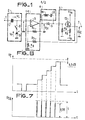
- means 2 for adjusting the limitation threshold receive, on the input terminal 1 of the device, a voltage composed of the addition of a luminance signal, and of a chrominance signal if it is color television ( Figure 2). These signals are transmitted by a capacitor C at the output of the means 2. This is connected by a switch 8 to the negative terminal of a generator 9 of direct voltage V p negative with respect to the reference potential.
- the switch 8 is controlled in synchronism with the luminance signal, so that it closes for the duration of the black plateau, T in FIG. 2.
- the capacitor is therefore charged at a voltage V equal to the voltage of the black level, minus the voltage V.
- the luminance signal V applied to the output of the means 2 thus has a black plateau voltage V N adjustable by acting on the value of V. If V changes in value the whole luminance signal is shifted.
- This signal is applied to the input of the amplification means 14 consisting of an operational amplifier 3 and of the resistors R 3 , R 4 and R 1 .
- the input terminal of the means 14 is the non-inverting input (+) of the operational amplifier 3.
- the inverting input (-) of the amplifier 3 is connected on the one hand to the output 7 of the device by the resistor R 3 to form a first feedback loop, on the other hand to the output of the amplifier 3 by resistance R 1 to form a second feedback loop.
- this input is connected to the reference potential by the resistor R 4 .
- the output of the amplifier 3 constitutes the output of the means 14. This is connected through a diode 5, in the cathode-anode direction, to the input of an amplifier 6.
- the latter has unity gain. It consists of an NPN transistor, mounted as a common collector. The base of the transistor constitutes the input of the amplifier and is connected to the reference potential by a resistor R 2 . The collector is connected directly to the positive terminal of the power supply (+ V A ).
- the transmitter is connected, through a resistor R 5 , to the terminal (-V A ) of a negative supply with respect to the reference potential. It constitutes the output of amplifier 6 and of the entire device.
- Diode 5 and resistor R 2 constitute a clipper.
- the anode potential of diode 5 is close to OV by neglecting the voltage created by the bias current of the base of the transistor (13) in the resistor R 2 .
- the diode 5 is blocked. The luminance signal is no longer transmitted. So that the chrominance signal is not affected, the diode is shunted by a bandpass filter 4, consisting of an inductor 11 and a capacitor 12, tuned to the frequency of the chrominance subcarrier .
- This gain is the same for the luminance signal and the chrominance signal.
- diode 5 is blocked because the signal has a greater amplitude or because the whole signal has been shifted to a higher potential by acting on the value of the voltage V p as explained above .
- the luminance signal is no longer transmitted to the amplifier 6.
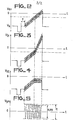
- the chrominance signal passes through the filter 4. It is amplified as in the first case. Because of the isolation caused by the diode, the luminance signal at output 7 no longer changes, it remains at a constant level to which the chrominance signal is added ( Figure 4).
- the second feedback loop is no longer active for the luminance signal. Resistor R J sees at output 7 a DC voltage generator with low internal resistance. Everything happens as if R 3 is in parallel with R 4 .
- the voltage gain, for the luminance signal seen at the output of amplifier 3, is then:
- R is chosen for example such that so
- the luminance signal is amplified about ten times greater than in the first case.
- the output impedance is of low value, but the presence of the amplifier 6 is not essential, it is within the reach of the skilled person to simplify the device by eliminating the transistor 13 and resistance R 5 .
- the output of the device is then constituted by the point common to the diode 5 and to the resistor R 2 .
- the me ires carried out on such a device show that the distortion rate of n, -linearity is less than 1% when the limitation threshold is adjusted to 0.3dB above the peak of the luminance signal.
- V I luminance signal
- FIG. 7 the same signal, after differentiation, V Id , to show and compare the amplitudes of the different levels.
- the differential gain distortion rate affecting the V SP subcarrier remains less than 1% beyond the limitation (FIG 5).
- the invention is not limited to the embodiment described and shown, in particular it is within the reach of ordinary skill in the art to adjust the level of clipping differently.
- the generator 9 can be connected otherwise.
- the switch 8 is directly connected to the reference terminal of the power supplies and the generator 9 is put in series with the resistor R 2 .
- By acting on the voltage supplied by this generator it is possible to modify the voltage present, at rest on the anode of diode 5, and thus adjust the level of limitation of the amplitude of the luminance signal.
- amplifier 6 it is within the reach of those skilled in the art to produce amplifier 6 differently, for example with a PNP transistor; or invert the diode 5 to limit negative luminance signals.
Landscapes
- Engineering & Computer Science (AREA)
- Multimedia (AREA)
- Signal Processing (AREA)
- Processing Of Color Television Signals (AREA)
- Television Receiver Circuits (AREA)
- Variable-Direction Aerials And Aerial Arrays (AREA)
- Details Of Aerials (AREA)
- Burglar Alarm Systems (AREA)
- Picture Signal Circuits (AREA)
Priority Applications (1)
| Application Number | Priority Date | Filing Date | Title |
|---|---|---|---|
| AT82400031T ATE13123T1 (de) | 1981-01-23 | 1982-01-08 | Leuchtdichtesignal-begrenzereinrichtung. |
Applications Claiming Priority (2)
| Application Number | Priority Date | Filing Date | Title |
|---|---|---|---|
| FR8101290 | 1981-01-23 | ||
| FR8101290A FR2498859A1 (fr) | 1981-01-23 | 1981-01-23 | Dispositif de limitation du signal de luminance et emetteur de television comportant un tel dispositif |
Publications (3)
| Publication Number | Publication Date |
|---|---|
| EP0057117A2 true EP0057117A2 (de) | 1982-08-04 |
| EP0057117A3 EP0057117A3 (en) | 1982-08-25 |
| EP0057117B1 EP0057117B1 (de) | 1985-05-02 |
Family
ID=9254456
Family Applications (1)
| Application Number | Title | Priority Date | Filing Date |
|---|---|---|---|
| EP82400031A Expired EP0057117B1 (de) | 1981-01-23 | 1982-01-08 | Leuchtdichtesignal-Begrenzereinrichtung |
Country Status (6)
| Country | Link |
|---|---|
| EP (1) | EP0057117B1 (de) |
| AT (1) | ATE13123T1 (de) |
| CA (1) | CA1196089A (de) |
| DE (1) | DE3263320D1 (de) |
| ES (1) | ES8302394A1 (de) |
| FR (1) | FR2498859A1 (de) |
Cited By (1)
| Publication number | Priority date | Publication date | Assignee | Title |
|---|---|---|---|---|
| EP2498052A3 (de) * | 2011-03-08 | 2014-08-06 | Honeywell International Inc. | Hochlinearer Signalverarbeitungsverstärker |
Family Cites Families (2)
| Publication number | Priority date | Publication date | Assignee | Title |
|---|---|---|---|---|
| US3393369A (en) * | 1965-10-22 | 1968-07-16 | Electronic Associates | Feedback limiter circuit having voltage gain amplifier |
| DE2048045A1 (de) * | 1970-09-30 | 1972-04-06 | Rohde & Schwarz | Schaltung zum Begrenzen des frequenzmässig unterhalb des Chrominanzanteiles liegenden Luminanzanteiles eines Farbfernsehsignales auf einen vorbestimmten Soll-Weisswert |
-
1981
- 1981-01-23 FR FR8101290A patent/FR2498859A1/fr active Granted
-
1982
- 1982-01-08 EP EP82400031A patent/EP0057117B1/de not_active Expired
- 1982-01-08 AT AT82400031T patent/ATE13123T1/de not_active IP Right Cessation
- 1982-01-08 DE DE8282400031T patent/DE3263320D1/de not_active Expired
- 1982-01-21 CA CA000394592A patent/CA1196089A/fr not_active Expired
- 1982-01-22 ES ES508974A patent/ES8302394A1/es not_active Expired
Cited By (1)
| Publication number | Priority date | Publication date | Assignee | Title |
|---|---|---|---|---|
| EP2498052A3 (de) * | 2011-03-08 | 2014-08-06 | Honeywell International Inc. | Hochlinearer Signalverarbeitungsverstärker |
Also Published As
| Publication number | Publication date |
|---|---|
| EP0057117B1 (de) | 1985-05-02 |
| ES508974A0 (es) | 1982-12-16 |
| ES8302394A1 (es) | 1982-12-16 |
| FR2498859A1 (fr) | 1982-07-30 |
| CA1196089A (fr) | 1985-10-29 |
| DE3263320D1 (en) | 1985-06-05 |
| EP0057117A3 (en) | 1982-08-25 |
| ATE13123T1 (de) | 1985-05-15 |
| FR2498859B1 (de) | 1984-02-24 |
Similar Documents
| Publication | Publication Date | Title |
|---|---|---|
| EP0016705B1 (de) | R.F.Stufe mit automatischer Verstärkungsregelung und Empfänger mit einer solchen Stufe | |
| EP0040127B1 (de) | Signalübertragungsanordnung mit einer Schaltung zur Vorkorrektur nichtlinearer Produkte | |
| FR2655219A1 (fr) | Dispositif de linearisation a predistorsion a action directe. | |
| FR2495870A1 (fr) | Dispositif de protection d'une diode laser | |
| US4450564A (en) | Apparatus for modulating the output signal of a converter | |
| EP0072721B1 (de) | System zur Lokalisierung von Kreisen und Unterbrechungen in einer Zweidrahtleitung | |
| EP0022015B1 (de) | Audioverstärker und Verfahren zur Audiofrequenzverstärkung | |
| FR2645377A1 (fr) | Circuit suppresseur d'interferences | |
| EP0057117B1 (de) | Leuchtdichtesignal-Begrenzereinrichtung | |
| EP0318379A1 (de) | Ultrahochfrequenzverstärker mit sehr breitem Durchlassbereich | |
| FR2561051A1 (fr) | Systeme de traitement de signaux video avec limiteur automatique des courants des faisceaux | |
| EP0081413B1 (de) | Retransmissionseinrichtung mit gemeinsamer Bild-/Tonträgerverstärkung und automatischer Steuerung des Bild-/Tonverhältnisses | |
| EP0064431B1 (de) | Vorrichtung zur Korrektur nichtlinearer Videofrequenz mit selektiver Zweckmässigkeit | |
| EP3866337A1 (de) | Audio-verstärker klasse ad | |
| FR2519174A1 (fr) | Circuit de reduction de bruit | |
| EP0377205A1 (de) | Strombegrenzer und seine Verwendung in einem optischen Empfänger | |
| FR2465228A1 (fr) | Systeme detecteur d'enveloppe d'un signal electrique | |
| FR2529035A1 (fr) | Dispositif d'amplification d'audiofrequences permettant un accroissement de la puissance moyenne d'ecoute | |
| EP0141715A2 (de) | Vorrichtung zur automatischen Vorkorrektur von Nichtlinearitäten in einer Leistungsverstärkerkette, sowie ihre Anwendung in einem Fernsehsender | |
| FR2538141A1 (fr) | Dispositif de limitation de l'amplitude d'un signal par ecretage superieur et inferieur | |
| JP4291006B2 (ja) | 光受信機 | |
| EP0052347B1 (de) | Vorverstärker mit Trägerstrom, Schalter zum Unterbrechen des Mikrophons und eine Vorrichtung zum Signalisieren dieser Unterbrechung enthaltender Fernsprechapparat | |
| FR2839165A1 (fr) | Appareil radioelectrique comportant un amplificateur pour signaux a radiofrequence, amplificateur pour signaux a radiofrequence et procede pour amplifier de tels signaux | |
| EP0028181A1 (de) | Vorrichtung zur Hochfrequenz-Vorkorrektur der Nichtlinearität in Signalverstärkern, wobei das Signal mindestens ein amplitudemoduliertes Trägersignal umfasst, und diese Vorrichtung enthaltender Fernsehsender | |
| FR2656179A1 (fr) | Demodulateur a boucle de phase. |
Legal Events
| Date | Code | Title | Description |
|---|---|---|---|
| PUAI | Public reference made under article 153(3) epc to a published international application that has entered the european phase |
Free format text: ORIGINAL CODE: 0009012 |
|
| PUAL | Search report despatched |
Free format text: ORIGINAL CODE: 0009013 |
|
| AK | Designated contracting states |
Designated state(s): AT BE CH DE GB IT LU NL SE |
|
| AK | Designated contracting states |
Designated state(s): AT BE CH DE GB IT LU NL SE |
|
| 17P | Request for examination filed |
Effective date: 19830114 |
|
| ITF | It: translation for a ep patent filed | ||
| GRAA | (expected) grant |
Free format text: ORIGINAL CODE: 0009210 |
|
| AK | Designated contracting states |
Designated state(s): AT BE CH DE GB IT LI LU NL SE |
|
| REF | Corresponds to: |
Ref document number: 13123 Country of ref document: AT Date of ref document: 19850515 Kind code of ref document: T |
|
| REF | Corresponds to: |
Ref document number: 3263320 Country of ref document: DE Date of ref document: 19850605 |
|
| PLBE | No opposition filed within time limit |
Free format text: ORIGINAL CODE: 0009261 |
|
| STAA | Information on the status of an ep patent application or granted ep patent |
Free format text: STATUS: NO OPPOSITION FILED WITHIN TIME LIMIT |
|
| 26N | No opposition filed | ||
| ITTA | It: last paid annual fee | ||
| EPTA | Lu: last paid annual fee | ||
| PGFP | Annual fee paid to national office [announced via postgrant information from national office to epo] |
Ref country code: CH Payment date: 19941216 Year of fee payment: 14 |
|
| PGFP | Annual fee paid to national office [announced via postgrant information from national office to epo] |
Ref country code: SE Payment date: 19941219 Year of fee payment: 14 Ref country code: GB Payment date: 19941219 Year of fee payment: 14 Ref country code: DE Payment date: 19941219 Year of fee payment: 14 |
|
| PGFP | Annual fee paid to national office [announced via postgrant information from national office to epo] |
Ref country code: LU Payment date: 19950101 Year of fee payment: 14 |
|
| PGFP | Annual fee paid to national office [announced via postgrant information from national office to epo] |
Ref country code: BE Payment date: 19950104 Year of fee payment: 14 |
|
| PGFP | Annual fee paid to national office [announced via postgrant information from national office to epo] |
Ref country code: AT Payment date: 19950130 Year of fee payment: 14 |
|
| EAL | Se: european patent in force in sweden |
Ref document number: 82400031.9 |
|
| PGFP | Annual fee paid to national office [announced via postgrant information from national office to epo] |
Ref country code: NL Payment date: 19950131 Year of fee payment: 14 |
|
| PG25 | Lapsed in a contracting state [announced via postgrant information from national office to epo] |
Ref country code: LU Free format text: LAPSE BECAUSE OF NON-PAYMENT OF DUE FEES Effective date: 19960108 Ref country code: GB Effective date: 19960108 Ref country code: AT Effective date: 19960108 |
|
| PG25 | Lapsed in a contracting state [announced via postgrant information from national office to epo] |
Ref country code: SE Effective date: 19960109 |
|
| PG25 | Lapsed in a contracting state [announced via postgrant information from national office to epo] |
Ref country code: LI Effective date: 19960131 Ref country code: CH Effective date: 19960131 Ref country code: BE Effective date: 19960131 |
|
| BERE | Be: lapsed |
Owner name: THOMSON-CSF Effective date: 19960131 |
|
| PG25 | Lapsed in a contracting state [announced via postgrant information from national office to epo] |
Ref country code: NL Effective date: 19960801 |
|
| GBPC | Gb: european patent ceased through non-payment of renewal fee |
Effective date: 19960108 |
|
| REG | Reference to a national code |
Ref country code: CH Ref legal event code: PL |
|
| NLV4 | Nl: lapsed or anulled due to non-payment of the annual fee |
Effective date: 19960801 |
|
| PG25 | Lapsed in a contracting state [announced via postgrant information from national office to epo] |
Ref country code: DE Effective date: 19961001 |
|
| EUG | Se: european patent has lapsed |
Ref document number: 82400031.9 |