EP0057253A2 - Bande de support de système comprenant plusieurs supports de système pour circuits intégrés - Google Patents
Bande de support de système comprenant plusieurs supports de système pour circuits intégrés Download PDFInfo
- Publication number
- EP0057253A2 EP0057253A2 EP81107910A EP81107910A EP0057253A2 EP 0057253 A2 EP0057253 A2 EP 0057253A2 EP 81107910 A EP81107910 A EP 81107910A EP 81107910 A EP81107910 A EP 81107910A EP 0057253 A2 EP0057253 A2 EP 0057253A2
- Authority
- EP
- European Patent Office
- Prior art keywords
- system carrier
- tape
- area
- recess
- carriers
- Prior art date
- Legal status (The legal status is an assumption and is not a legal conclusion. Google has not performed a legal analysis and makes no representation as to the accuracy of the status listed.)
- Granted
Links
Images


Classifications
-
- H—ELECTRICITY
- H05—ELECTRIC TECHNIQUES NOT OTHERWISE PROVIDED FOR
- H05K—PRINTED CIRCUITS; CASINGS OR CONSTRUCTIONAL DETAILS OF ELECTRIC APPARATUS; MANUFACTURE OF ASSEMBLAGES OF ELECTRICAL COMPONENTS
- H05K3/00—Apparatus or processes for manufacturing printed circuits
- H05K3/0097—Processing two or more printed circuits simultaneously, e.g. made from a common substrate, or temporarily stacked circuit boards
-
- H—ELECTRICITY
- H10—SEMICONDUCTOR DEVICES; ELECTRIC SOLID-STATE DEVICES NOT OTHERWISE PROVIDED FOR
- H10W—GENERIC PACKAGES, INTERCONNECTIONS, CONNECTORS OR OTHER CONSTRUCTIONAL DETAILS OF DEVICES COVERED BY CLASS H10
- H10W70/00—Package substrates; Interposers; Redistribution layers [RDL]
- H10W70/40—Leadframes
- H10W70/453—Leadframes comprising flexible metallic tapes
-
- H—ELECTRICITY
- H05—ELECTRIC TECHNIQUES NOT OTHERWISE PROVIDED FOR
- H05K—PRINTED CIRCUITS; CASINGS OR CONSTRUCTIONAL DETAILS OF ELECTRIC APPARATUS; MANUFACTURE OF ASSEMBLAGES OF ELECTRICAL COMPONENTS
- H05K1/00—Printed circuits
- H05K1/02—Details
- H05K1/03—Use of materials for the substrate
- H05K1/0393—Flexible materials
-
- H—ELECTRICITY
- H05—ELECTRIC TECHNIQUES NOT OTHERWISE PROVIDED FOR
- H05K—PRINTED CIRCUITS; CASINGS OR CONSTRUCTIONAL DETAILS OF ELECTRIC APPARATUS; MANUFACTURE OF ASSEMBLAGES OF ELECTRICAL COMPONENTS
- H05K2201/00—Indexing scheme relating to printed circuits covered by H05K1/00
- H05K2201/09—Shape and layout
- H05K2201/09009—Substrate related
- H05K2201/09063—Holes or slots in insulating substrate not used for electrical connections
-
- H—ELECTRICITY
- H05—ELECTRIC TECHNIQUES NOT OTHERWISE PROVIDED FOR
- H05K—PRINTED CIRCUITS; CASINGS OR CONSTRUCTIONAL DETAILS OF ELECTRIC APPARATUS; MANUFACTURE OF ASSEMBLAGES OF ELECTRICAL COMPONENTS
- H05K2201/00—Indexing scheme relating to printed circuits covered by H05K1/00
- H05K2201/09—Shape and layout
- H05K2201/09009—Substrate related
- H05K2201/0909—Preformed cutting or breaking line
-
- H—ELECTRICITY
- H05—ELECTRIC TECHNIQUES NOT OTHERWISE PROVIDED FOR
- H05K—PRINTED CIRCUITS; CASINGS OR CONSTRUCTIONAL DETAILS OF ELECTRIC APPARATUS; MANUFACTURE OF ASSEMBLAGES OF ELECTRICAL COMPONENTS
- H05K2203/00—Indexing scheme relating to apparatus or processes for manufacturing printed circuits covered by H05K3/00
- H05K2203/15—Position of the PCB during processing
- H05K2203/1545—Continuous processing, i.e. involving rolls moving a band-like or solid carrier along a continuous production path
-
- H—ELECTRICITY
- H05—ELECTRIC TECHNIQUES NOT OTHERWISE PROVIDED FOR
- H05K—PRINTED CIRCUITS; CASINGS OR CONSTRUCTIONAL DETAILS OF ELECTRIC APPARATUS; MANUFACTURE OF ASSEMBLAGES OF ELECTRICAL COMPONENTS
- H05K3/00—Apparatus or processes for manufacturing printed circuits
- H05K3/0011—Working of insulating substrates or insulating layers
- H05K3/0044—Mechanical working of the substrate, e.g. drilling or punching
- H05K3/0052—Depaneling, i.e. dividing a panel into circuit boards; Working of the edges of circuit boards
Definitions
- the invention relates to a system carrier tape with a plurality of system carriers for integrated circuits arranged one behind the other at a distance in the longitudinal direction of the tape, each of which consists of a number of conductor tracks which radiate from an inner area assigned to the integrated circuit to an outer area having connection surfaces. Between the band edge and the band edge adjacent to it there is a band edge area serving to transport the band during manufacture.
- System carriers for integrated circuits consist of a film-like insulating substrate on which the conductor tracks of the system carrier are applied.
- System carriers of this type are produced in a continuous photoetching process from a metal-clad, if they are required in large numbers Insulating tape or in a continuous screen printing process.
- the system carrier belt passes through several production stages, whereby it is generally transported in the manner of a film and consequently has a perforation in its two edge areas.
- System carrier tapes are also known in which the individual system carriers are connected to one another directly and without an insulating material tape, that is to say the entire system carrier tape consists entirely of metal.
- the system carrier tape whatever its structure, is a kind of semi-finished product. After soldering or, which is generally preferred for manufacturing reasons, welding the conductor tracks to the integrated circuit and, if necessary, applying a plastic fixture - both are also carried out in one continuous process, during which the system carrier tape is also transported in film form - the system carrier is punched out of the system carrier tape and then the connecting lines for the other circuit elements can be soldered or welded onto the outer connection surfaces.
- the invention takes a different approach to remedying these disadvantages, and it is proposed according to the invention to provide at least one recess which increases the flexibility of the belt in this area between two adjacent system carriers and the two band edge regions assigned to these system carriers.
- the arrangement of one or more such recesses between the system carriers in the system carrier belt results in a caterpillar effect: the individual system carriers are articulated with one another via the well-flexible intermediate pieces the connected, so that when the belt bends, the individual belt sections having the system carriers are not, or only to a negligible extent, subjected to bending, while the areas lying between the system carriers absorb the entire band deflection between two system carriers. This ensures that when the band bends, the forces acting on the connection between the conductor tracks of the system carrier and the integrated circuit remain so small that the connection is no longer separated.
- the embodiment with two or more recesses in each area has the advantage, however, that the system carrier tape can be subjected to greater forces acting in the longitudinal direction during production than is the case with a system carrier tape in which only one in each area only one from Band area to band area and recess extending from system carrier to system carrier is present.
- An embodiment lying between the two aforementioned embodiments with regard to resilience and flexibility consists in that at least two recesses which are parallel to one another and arranged one behind the other in the longitudinal direction of the strip are present in the area.
- each recess end facing a band edge region has at least one recess extension extending approximately in the longitudinal direction of the band between the band edge region and the system carrier.
- each system carrier is connected to the band edge area exclusively via two narrow bridges running transversely to the longitudinal axis of the band. Furthermore, it has proven to be It has proven to be expedient to arrange the two bridges approximately in the middle of the system carrier in order to obtain a secure mounting of the system carrier in the system carrier band on the one hand and on the other hand to eliminate the torsional forces that may occur when the bridges are offset in the system carrier when the band bends.
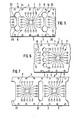
- the known system carrier tape shown in FIG. 1 consists of a film-like insulating substrate 1, which in its edge regions 2 and 3 each has perforations 4 and 5 for transporting the tape through the various manufacturing devices.
- the system carriers 6 are located one behind the other in the longitudinal direction on the film-like insulating material substrate 1.
- Each system carrier consists of a number of electrically conductive outer connection surfaces 7 and conductor tracks 8 extending from these, the ends 9 of which form the connections for the integrated circuits 10.
- the connection surfaces 7 and the parts of the conductor tracks 8 which extend between the connection surfaces 7 and the boundary lines 11 of the substrate are in fixed connection with the film-like insulating substrate 1, while the conductor tracks from the boundary lines 11 of the substrate 1 to the ends 9 have no connection with the substrate 1, since this is removed between the boundary lines 11.
- connection of the conductor ends 9 with the corresponding pads on the integrated Circuit 10 is accomplished by welding in a single operation. Then the system carriers 6 with the applied integrated circuits 10 are punched out of the film-like insulating material substrate along the dashed lines 12.
- the highly flexible zones 13 are each implemented by five slots 14 running transversely to the longitudinal axis of the strip.
- the length of these slots is chosen to be substantially smaller than the distance between the two edge regions 2 and 3.
- the flexibility of the strip in the region of the flexible zone 13 is greater than in the embodiment according to FIG. 2, however, the load capacity of such a system carrier tape is limited to tensile forces of a smaller extent.
- zone 13 is finally realized by a single recess 17 which extends from one band edge area 2 to the other band edge area 3 and at its ends adjacent to the band edge areas 2 and 3 each in two narrow, in the longitudinal direction of the System carrier tape extending recess extensions 18 and 19 passes.
- the recesses 22 consist of a narrow middle part 23 which is widened at the ends 24 and 25 respectively transforms.
- this embodiment stands between the embodiment according to FIG. 4 and that of FIG. 7, in which there is only one wide recess 27 between two adjacent system carriers 6.
- Such a belt can be loaded with relatively high tensile forces.
Landscapes
- Engineering & Computer Science (AREA)
- Manufacturing & Machinery (AREA)
- Microelectronics & Electronic Packaging (AREA)
- Wire Bonding (AREA)
- Packages (AREA)
Applications Claiming Priority (2)
| Application Number | Priority Date | Filing Date | Title |
|---|---|---|---|
| DE3103454 | 1981-02-02 | ||
| DE19813103454 DE3103454A1 (de) | 1981-02-02 | 1981-02-02 | Systemtraegerband mit mehreren systemtraegern fuer integrierte schaltkreise |
Publications (3)
| Publication Number | Publication Date |
|---|---|
| EP0057253A2 true EP0057253A2 (fr) | 1982-08-11 |
| EP0057253A3 EP0057253A3 (en) | 1982-09-01 |
| EP0057253B1 EP0057253B1 (fr) | 1985-02-27 |
Family
ID=6123850
Family Applications (1)
| Application Number | Title | Priority Date | Filing Date |
|---|---|---|---|
| EP81107910A Expired EP0057253B1 (fr) | 1981-02-02 | 1981-10-05 | Bande de support de système comprenant plusieurs supports de système pour circuits intégrés |
Country Status (3)
| Country | Link |
|---|---|
| EP (1) | EP0057253B1 (fr) |
| JP (1) | JPS57147263A (fr) |
| DE (1) | DE3103454A1 (fr) |
Cited By (6)
| Publication number | Priority date | Publication date | Assignee | Title |
|---|---|---|---|---|
| WO1986006212A1 (fr) * | 1985-04-12 | 1986-10-23 | Hughes Aircraft Company | Matrice a fentes avec supports de mini-puces |
| US4762606A (en) * | 1985-04-12 | 1988-08-09 | Hughes Aircraft Company | Mini chip carrier slotted array |
| US4802277A (en) * | 1985-04-12 | 1989-02-07 | Hughes Aircraft Company | Method of making a chip carrier slotted array |
| EP0499748A1 (fr) * | 1990-12-27 | 1992-08-26 | International Business Machines Corporation | Bande du type TAB |
| EP1136936A1 (fr) * | 2000-03-24 | 2001-09-26 | Infineon Technologies AG | Boítier pour capteurs biométriques en puce |
| US6744120B1 (en) * | 1999-03-11 | 2004-06-01 | Seiko Epson Corporation | Flexible interconnect substrate of a tape-shaped semiconductor device, semiconductor device and circuit board |
Families Citing this family (4)
| Publication number | Priority date | Publication date | Assignee | Title |
|---|---|---|---|---|
| DE19525686C2 (de) * | 1995-07-14 | 2002-02-21 | Alcatel Kabel Ag | Vorrichtung zur Signalübertragung zwischen zwei Endstellen |
| JP2755229B2 (ja) * | 1995-10-06 | 1998-05-20 | セイコーエプソン株式会社 | 電子回路基板部品 |
| DE19910131C2 (de) * | 1999-03-01 | 2002-08-29 | Takata Petri Ag | Einrichtung zur Übertragung elektrischen Stroms |
| JP2001237280A (ja) | 2000-02-22 | 2001-08-31 | Nec Corp | テープキャリア型半導体装置および可撓性フィルム接続基板 |
Family Cites Families (2)
| Publication number | Priority date | Publication date | Assignee | Title |
|---|---|---|---|---|
| US4012766A (en) * | 1973-08-28 | 1977-03-15 | Western Digital Corporation | Semiconductor package and method of manufacture thereof |
| DE3061383D1 (en) * | 1979-02-19 | 1983-01-27 | Fujitsu Ltd | Semiconductor device and method for manufacturing the same |
-
1981
- 1981-02-02 DE DE19813103454 patent/DE3103454A1/de not_active Withdrawn
- 1981-10-05 EP EP81107910A patent/EP0057253B1/fr not_active Expired
-
1982
- 1982-02-01 JP JP57013421A patent/JPS57147263A/ja active Pending
Cited By (8)
| Publication number | Priority date | Publication date | Assignee | Title |
|---|---|---|---|---|
| WO1986006212A1 (fr) * | 1985-04-12 | 1986-10-23 | Hughes Aircraft Company | Matrice a fentes avec supports de mini-puces |
| US4762606A (en) * | 1985-04-12 | 1988-08-09 | Hughes Aircraft Company | Mini chip carrier slotted array |
| US4802277A (en) * | 1985-04-12 | 1989-02-07 | Hughes Aircraft Company | Method of making a chip carrier slotted array |
| EP0499748A1 (fr) * | 1990-12-27 | 1992-08-26 | International Business Machines Corporation | Bande du type TAB |
| US5288539A (en) * | 1990-12-27 | 1994-02-22 | International Business Machines, Corp. | Tab tape with a peeling-prevention structure for the conductive layer |
| US6744120B1 (en) * | 1999-03-11 | 2004-06-01 | Seiko Epson Corporation | Flexible interconnect substrate of a tape-shaped semiconductor device, semiconductor device and circuit board |
| EP1136936A1 (fr) * | 2000-03-24 | 2001-09-26 | Infineon Technologies AG | Boítier pour capteurs biométriques en puce |
| WO2001073678A1 (fr) * | 2000-03-24 | 2001-10-04 | Infineon Technologies Ag | Boitier pour puces de detection biometriques |
Also Published As
| Publication number | Publication date |
|---|---|
| JPS57147263A (en) | 1982-09-11 |
| EP0057253B1 (fr) | 1985-02-27 |
| EP0057253A3 (en) | 1982-09-01 |
| DE3103454A1 (de) | 1982-08-26 |
Similar Documents
| Publication | Publication Date | Title |
|---|---|---|
| DE3123198C2 (de) | Trägerelemente für einen IC-Baustein | |
| DE69131712T2 (de) | Lottragender anschlussdraht | |
| DE4310288B4 (de) | Oberflächenmontierbarer Widerstand | |
| DE2726040C3 (de) | Hochfrequenz-Halbleiteranordnung | |
| EP0374648B1 (fr) | Dispositif de connexion d'un câble électrique | |
| DE19920593B4 (de) | Chipträger für ein Chipmodul und Verfahren zur Herstellung des Chipmoduls | |
| DE2100103A1 (de) | Abgeschirmte Halbleiter Vorrichtung | |
| EP0115803A2 (fr) | Cellule photovoltaique en forme de disque | |
| DE68905475T2 (de) | Halbleiter-speichermodul hoeher dichte. | |
| DE1277595B (de) | Elektronisches Schaltungsbauelement und aus gleichen Bauelementen bestehende Baugruppe fuer elektronische Rechenmaschinen | |
| EP0057253B1 (fr) | Bande de support de système comprenant plusieurs supports de système pour circuits intégrés | |
| DE2315711A1 (de) | Verfahren zum kontaktieren von in einem halbleiterkoerper untergebrachten integrierten schaltungen mit hilfe eines ersten kontaktierungsrahmens | |
| DE3912697A1 (de) | Stoerschutzfilter | |
| DE69624469T2 (de) | Matrix von mit elektrischen bauelementen angeschlossenen fahnen und entsprechendes verfahren zum anschluss | |
| DE2726697C2 (de) | Nachgiebige Folie mit an ihr haftenden elektrischen Leitungen | |
| DE3909528A1 (de) | Stoerschutzfilter | |
| DE19732807B4 (de) | Integriertes Schaltungsbauelement | |
| DE2837318C2 (de) | Anordnung zur Herstellung einer elektrischen Verbindung | |
| DE69516445T2 (de) | Elektrodenanordnung für kontinuierlich arbeitenden Tintenstrahldrucker | |
| DE2303537A1 (de) | Anschlusschiene und verfahren zu ihrer herstellung | |
| DE3316914C2 (de) | Reihenanordnung elektronischer Bauelemente | |
| EP1075027A2 (fr) | Contact d'interconnections métalliques d'une puce semiconductrice intégrée | |
| DE3721661A1 (de) | Verbindungsband | |
| DE3022590C2 (de) | Verfahren zum Anbringen und Befestigen von parallel zueinander verlaufenden Stromzuführungsdrähten an gegenüber befindlichen Seitenflächen elektrischer Bauelemente | |
| DE2114075A1 (de) | Trockenelektrolytkondensator und Verfahren zu seiner Herstellung |
Legal Events
| Date | Code | Title | Description |
|---|---|---|---|
| PUAI | Public reference made under article 153(3) epc to a published international application that has entered the european phase |
Free format text: ORIGINAL CODE: 0009012 |
|
| PUAL | Search report despatched |
Free format text: ORIGINAL CODE: 0009013 |
|
| AK | Designated contracting states |
Designated state(s): FR GB IT NL SE |
|
| AK | Designated contracting states |
Designated state(s): FR GB IT NL SE |
|
| 17P | Request for examination filed |
Effective date: 19820819 |
|
| ITF | It: translation for a ep patent filed | ||
| GRAA | (expected) grant |
Free format text: ORIGINAL CODE: 0009210 |
|
| AK | Designated contracting states |
Designated state(s): FR GB IT NL SE |
|
| ET | Fr: translation filed | ||
| PG25 | Lapsed in a contracting state [announced via postgrant information from national office to epo] |
Ref country code: SE Effective date: 19851006 |
|
| PLBE | No opposition filed within time limit |
Free format text: ORIGINAL CODE: 0009261 |
|
| STAA | Information on the status of an ep patent application or granted ep patent |
Free format text: STATUS: NO OPPOSITION FILED WITHIN TIME LIMIT |
|
| 26N | No opposition filed | ||
| PG25 | Lapsed in a contracting state [announced via postgrant information from national office to epo] |
Ref country code: NL Effective date: 19860501 |
|
| GBPC | Gb: european patent ceased through non-payment of renewal fee | ||
| PG25 | Lapsed in a contracting state [announced via postgrant information from national office to epo] |
Ref country code: FR Free format text: LAPSE BECAUSE OF NON-PAYMENT OF DUE FEES Effective date: 19860630 |
|
| NLV4 | Nl: lapsed or anulled due to non-payment of the annual fee | ||
| REG | Reference to a national code |
Ref country code: FR Ref legal event code: ST |
|
| PG25 | Lapsed in a contracting state [announced via postgrant information from national office to epo] |
Ref country code: GB Effective date: 19881121 |
|
| EUG | Se: european patent has lapsed |
Ref document number: 81107910.2 Effective date: 19860730 |