EP0058593B1 - Matrixanzeigevorrichtung mit verschiedenen Arten von Elektroden und Verfahren zu ihrer Ansteuerung - Google Patents
Matrixanzeigevorrichtung mit verschiedenen Arten von Elektroden und Verfahren zu ihrer Ansteuerung Download PDFInfo
- Publication number
- EP0058593B1 EP0058593B1 EP82400167A EP82400167A EP0058593B1 EP 0058593 B1 EP0058593 B1 EP 0058593B1 EP 82400167 A EP82400167 A EP 82400167A EP 82400167 A EP82400167 A EP 82400167A EP 0058593 B1 EP0058593 B1 EP 0058593B1
- Authority
- EP
- European Patent Office
- Prior art keywords
- electrodes
- electrode
- display device
- potential
- sets
- Prior art date
- Legal status (The legal status is an assumption and is not a legal conclusion. Google has not performed a legal analysis and makes no representation as to the accuracy of the status listed.)
- Expired
Links
Images
Classifications
-
- G—PHYSICS
- G02—OPTICS
- G02F—OPTICAL DEVICES OR ARRANGEMENTS FOR THE CONTROL OF LIGHT BY MODIFICATION OF THE OPTICAL PROPERTIES OF THE MEDIA OF THE ELEMENTS INVOLVED THEREIN; NON-LINEAR OPTICS; FREQUENCY-CHANGING OF LIGHT; OPTICAL LOGIC ELEMENTS; OPTICAL ANALOGUE/DIGITAL CONVERTERS
- G02F1/00—Devices or arrangements for the control of the intensity, colour, phase, polarisation or direction of light arriving from an independent light source, e.g. switching, gating or modulating; Non-linear optics
- G02F1/01—Devices or arrangements for the control of the intensity, colour, phase, polarisation or direction of light arriving from an independent light source, e.g. switching, gating or modulating; Non-linear optics for the control of the intensity, phase, polarisation or colour
- G02F1/13—Devices or arrangements for the control of the intensity, colour, phase, polarisation or direction of light arriving from an independent light source, e.g. switching, gating or modulating; Non-linear optics for the control of the intensity, phase, polarisation or colour based on liquid crystals, e.g. single liquid crystal display cells
- G02F1/133—Constructional arrangements; Operation of liquid crystal cells; Circuit arrangements
- G02F1/1333—Constructional arrangements; Manufacturing methods
- G02F1/1343—Electrodes
- G02F1/134309—Electrodes characterised by their geometrical arrangement
- G02F1/134336—Matrix
-
- G—PHYSICS
- G02—OPTICS
- G02F—OPTICAL DEVICES OR ARRANGEMENTS FOR THE CONTROL OF LIGHT BY MODIFICATION OF THE OPTICAL PROPERTIES OF THE MEDIA OF THE ELEMENTS INVOLVED THEREIN; NON-LINEAR OPTICS; FREQUENCY-CHANGING OF LIGHT; OPTICAL LOGIC ELEMENTS; OPTICAL ANALOGUE/DIGITAL CONVERTERS
- G02F1/00—Devices or arrangements for the control of the intensity, colour, phase, polarisation or direction of light arriving from an independent light source, e.g. switching, gating or modulating; Non-linear optics
- G02F1/01—Devices or arrangements for the control of the intensity, colour, phase, polarisation or direction of light arriving from an independent light source, e.g. switching, gating or modulating; Non-linear optics for the control of the intensity, phase, polarisation or colour
- G02F1/13—Devices or arrangements for the control of the intensity, colour, phase, polarisation or direction of light arriving from an independent light source, e.g. switching, gating or modulating; Non-linear optics for the control of the intensity, phase, polarisation or colour based on liquid crystals, e.g. single liquid crystal display cells
- G02F1/133—Constructional arrangements; Operation of liquid crystal cells; Circuit arrangements
- G02F1/1333—Constructional arrangements; Manufacturing methods
- G02F1/1343—Electrodes
- G02F1/134309—Electrodes characterised by their geometrical arrangement
- G02F1/134345—Subdivided pixels, e.g. for grey scale or redundancy
Definitions
- the present invention relates to a matrix display device with several sets of electrodes and its control method. It finds an application in opto-electronics, and mainly in the control of liquid crystal cells used in particular as converters of electrical information into optical information, in the processing of optical images in real time, in the production of colored filters which can be used in particular in color television, and in analog display.
- the present matrix display device comprises a display cell constituted by two transparent insulating walls and by an electro-optical material comprising a plurality of zones distributed in a matrix and interposed between a first system of electrodes covering one of the two walls and defining p control columns and a second system of electrodes covering the other wall, made up of parallel conductive strips, and defining q control lines, column x ,, where i is an integer such that 1 ⁇ i ⁇ p and the line y j , where j is an integer such that 1 ⁇ j ⁇ 1 defining an area xyj of the material, and comprises means making it possible to deliver on the lines and the columns appropriate excitation signals serving to excite a property material optics.
- the invention applies particularly well to such devices but it applies more generally to any device comprising a material of which an optical property can be modified by means of an electrical excitation.
- the material can be a solid or liquid, amorphous or crystalline body.
- the optical property can be an opacity, a refractive index, a transparency, an absorption, a diffusion, a diffraction, a convergence, a rotatory power, a birefringence, an intensity reflected in a determined solids angle, etc.
- known display consists for example in the case of a liquid crystal cell where the excitation is of an electrical nature, to be applied to the line x, a periodic voltage V x of zero mean value and to the other lines a zero voltage and to apply to the columns y j periodic voltages V yj of zero mean value, of the same duration and of the same frequency as the voltage V x but which are phase shifted with respect to them by an amount ⁇ ji .
- This phase shift ⁇ ji makes it possible to vary the intensity of the signal to be displayed, that is to say makes it possible to obtain different levels of gray.
- a binary display is obviously obtained by applying on the lines x ; the same scanning voltages Vx and by applying to the columns y j voltages V yj of the same duration, of the same frequency as V x , either in phase or in phase opposition with respect to V x , as desired display white or black.
- the present invention relates to a display device with several sets of electrodes and its control method making it possible in particular to limit the number of control circuits of the device and to simplify these circuits.
- the present invention relates to a matrix display device comprising a display cell made up of two insulating walls, and of an electro-optical material comprising a plurality of zones distributed in matrix and inter-. wedged between a first system of electrodes covering one of the two walls and defining p control columns and a second system of electrodes covering the other wall, made up of parallel conductive strips, and defining q control lines, the column x ; , where i is an integer whatever 1 ⁇ i ⁇ p and the line y j , where j is an integer such as 1 ⁇ j ⁇ q defining an area x i Y j of the material, and comprising means making it possible to deliver on the rows and columns of the appropriate excitation signals, said material having an optical property dependent on said excitation.
- the first electrode system comprises n sets of electrodes arranged and grouped so that each set consists of two sets of electrodes and that the choice of one set of each set corresponds to a control column and only one, the n sets of electrodes being arranged one above the other and electrically isolated from each other, each set comprising p / 2 k electrodes electrically connected together, where k is an integer different from a set of the other such as 1 ⁇ k ⁇ n.
- the first electrode system further comprises a full-layer electrode disposed directly on the corresponding insulating wall under the n sets of electrodes and electrically insulated from said sets of electrodes and in that the means making it possible to control the optical property of the material of the area X i Y j include means for applying a potential -V 1 on the full-layer electrode and a potential -V o on all the sets d 'electrodes except that which corresponds to column x ,, said assembly being set to high impedance, and means for applying to line y j a potential V 2 such that the voltage V 2 + V l corresponds to the desired value of the optical property of the material in the area x i Y j and that the voltage V 2 + V O is less than the excitation voltage of the optical property of the material.
- the material is a liquid crystal film whose optical property depends on the electric field applied to it.
- the present invention also relates to a method for controlling a matrix display device as defined above.
- This process is characterized in that, to control the optical property of the material of the area x i y j, a potential -V 1 is applied to the full-layer electrode and a potential -V o to all the sets of electrodes except that which corresponds to column x i , said assembly being set to high impedance and a potential V 2 such that the voltage V 2 + V 1 is applied to the line Y j corresponds to the desired value of the optical property of the material in the area X i V j and that the voltage V 2 + V O is less than the excitation voltage of the optical property of the material.
- the q zones of the same column x j are simultaneously controlled by simultaneously applying the potential V 2 to each row.
- the description refers to a display device comprising as material a liquid crystal film, the optical property of which depends on the electric field applied to it.
- the invention is of much more general application, but these display devices being currently well known and widely used, it is preferable to make the description on this example.
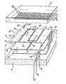
- This figure schematically represents a display cell comprising two insulating walls 2 and 4, generally transparent such as glass walls, arranged on either side of a shim of thickness 6, made of insulating material, defining a volume 8 which is occupied, when the cell is mounted by the material for which an optical property is controlled, for example a liquid crystal film.
- a first system of electrodes 10 defining p columns for controlling the optical property of the display material
- a second system of electrodes made up of transparent parallel conductive strips, denoted y j and defining q control lines of said optical property.
- These two electrode systems can be made of indium oxide.
- the dimensions and in particular the thickness of this system have not been respected.
- the n sets of electrodes each consist of two sets of electrodes referenced a and b. The electrodes are grouped so that the choice of one set in each set corresponds to only one column for controlling the optical property of the display material, the grouping of the electrodes will be described later
- the n sets of electrodes are arranged one above the other and above the full-layer electrode 12. These n sets of electrodes are electrically isolated from each other and isolated from the full-layer electrode by means of insulating layers such as 17 interposed between each set and the electrode 12.
- Each set of electrodes a or b of the k th set of electrodes comprises p / 2 k electrodes, k being an integer such that 1 k k n n and p the number of control columns of the display device.
- n an integer such that 1 k k n n and p the number of control columns of the display device.
- the set referenced 14 corresponds to k equal to one
- the set referenced 16 to k equal to two.
- the use of two sets of electrodes, corresponding to four control columns results in the assembly a or b of the set 14 comprising two electrodes referenced a 1 and a 2 or b 1 and b 2 and in that the set a or b of the set 16 comprises an electrode a or b.
- the two sets of electrodes are ordered according to the decreasing values of the integer k.
- the electrodes of the same set are electrically connected to each other, preferably by means of connections such as 18 and 20 as shown in the figure.
- the electrode b 1 is interposed between the electrode a 1 and the electrode a 2 and opposite the connection 20 connecting said electrodes a 1 and a 2
- the electrode a 2 is interposed between the electrode b 1 and b 2 and facing the connection 18 connecting said electrodes b 1 and b 2 .
- the liquid crystal zone between the line electrode y j and the group of electrodes x can be identified by the notation x i y j .
- the excitation of a zone X i Y j ' that is to say the control of an optical property of the liquid crystal contained in this zone, is carried out by applying to the groups of electrodes x, and to the line electrodes y j potentials, delivered by electric power sources, not shown, which cause the appearance of an electric field within the liquid crystal.
- An image is thus made to appear over the entire cell by defining it point by point and by exciting the zones one after the other according to the known principles of sequential control.
- the phenomenon used is the collective orientation of the molecules of said crystal parallel to the electrodes when said crystal is subjected to an electric field.
- the phenomenon used in such a device is described in French Patent No. 2,279,123, previously cited.
- the excitation of a zone X i V j of the material is carried out by applying to the line Y j of the second electrode system a potential V 2 and to the full layer electrode 12 a potential - V i .
- the group of electrodes x i is set to high impedance, that is to say electrically isolated, and the other groups are brought to a potential -V o such that V o is less than V,.
- one of the two sets of each set of electrodes is brought to the potential -V o and the other set is set to high impedance.
- the excitation of the material located opposite the electrode a 1 is done by bringing to the potential -V o the set b of the sets of electrodes 14 and 16 and by putting in high impedance the set a of the two sets 14 and 16, the full-layer electrode 12 being maintained at the potential -V 1 .
- the corresponding zone x i y j of the liquid crystal sees at its terminals a voltage little different from V 2 + V 1 , provided that the insulating layers 17 have a small thickness compared to that of the liquid crystal and / or a very dielectric constant higher than that of liquid crystal; this follows from the continuity of the electric field on the different electrodes of the same group. Furthermore, since the liquid crystal used has a threshold effect, the voltage V 2 + V 1 must be greater than the threshold voltage of said crystal. Similarly, the other zones of the liquid crystal facing the line y j see at their terminals a voltage V 2 + V o , a voltage which must be less than the threshold voltage of the liquid crystal.
- the potential V 2 corresponding to the value of the optical property which it is desired to display at the intersection point of this electrode is applied simultaneously to each row electrode. row and column x ,.
- the phenomenon used in such a display device being the collective orientation of the molecules by the action of an electric field on their dipole moment, to avoid any disturbance in the liquid due in particular to ion transits (polarization phenomenon) there It is necessary to reverse the voltage applied across the material, so the potentials applied to the two electrode systems.
- alternating voltages can be used to control the optical property of the material.
Landscapes
- Physics & Mathematics (AREA)
- Nonlinear Science (AREA)
- Geometry (AREA)
- Mathematical Physics (AREA)
- Chemical & Material Sciences (AREA)
- Crystallography & Structural Chemistry (AREA)
- General Physics & Mathematics (AREA)
- Optics & Photonics (AREA)
- Devices For Indicating Variable Information By Combining Individual Elements (AREA)
- Liquid Crystal (AREA)
Claims (7)
Applications Claiming Priority (2)
| Application Number | Priority Date | Filing Date | Title |
|---|---|---|---|
| FR8102219 | 1981-02-05 | ||
| FR8102219A FR2499276A1 (fr) | 1981-02-05 | 1981-02-05 | Dispositif d'affichage matriciel a plusieurs jeux d'electrodes et son procede de commande |
Publications (2)
| Publication Number | Publication Date |
|---|---|
| EP0058593A1 EP0058593A1 (de) | 1982-08-25 |
| EP0058593B1 true EP0058593B1 (de) | 1985-11-06 |
Family
ID=9254864
Family Applications (1)
| Application Number | Title | Priority Date | Filing Date |
|---|---|---|---|
| EP82400167A Expired EP0058593B1 (de) | 1981-02-05 | 1982-01-29 | Matrixanzeigevorrichtung mit verschiedenen Arten von Elektroden und Verfahren zu ihrer Ansteuerung |
Country Status (6)
| Country | Link |
|---|---|
| US (1) | US4509828A (de) |
| EP (1) | EP0058593B1 (de) |
| JP (1) | JPS57147681A (de) |
| CA (1) | CA1196415A (de) |
| DE (1) | DE3267210D1 (de) |
| FR (1) | FR2499276A1 (de) |
Families Citing this family (17)
| Publication number | Priority date | Publication date | Assignee | Title |
|---|---|---|---|---|
| FR2541027A1 (fr) * | 1983-02-16 | 1984-08-17 | Commissariat Energie Atomique | Imageur matriciel a dispositif de compensation du couplage entre les lignes et les colonnes |
| US4602850A (en) * | 1984-03-08 | 1986-07-29 | Vidium, Inc. | Light valve display having integrated driving circuits and shield electrode |
| US4728172A (en) * | 1984-08-08 | 1988-03-01 | Energy Conversion Devices, Inc. | Subassemblies for displays having pixels with two portions and capacitors |
| US4639087A (en) * | 1984-08-08 | 1987-01-27 | Energy Conversion Devices, Inc. | Displays having pixels with two portions and capacitors |
| DE3524085A1 (de) * | 1985-07-05 | 1987-01-08 | Vdo Schindling | Fluessigkristallzelle |
| NL9000942A (nl) * | 1990-04-20 | 1991-11-18 | Philips Nv | Weergeefinrichting. |
| KR100343376B1 (ko) * | 1993-12-31 | 2002-11-23 | 고려화학 주식회사 | 반도체소자봉지용경화제의제조방법및이를함유하는반도체소자봉지용수지조성물 |
| US7583251B2 (en) | 1995-07-20 | 2009-09-01 | E Ink Corporation | Dielectrophoretic displays |
| US7106296B1 (en) * | 1995-07-20 | 2006-09-12 | E Ink Corporation | Electronic book with multiple page displays |
| US7167155B1 (en) | 1995-07-20 | 2007-01-23 | E Ink Corporation | Color electrophoretic displays |
| US8139050B2 (en) * | 1995-07-20 | 2012-03-20 | E Ink Corporation | Addressing schemes for electronic displays |
| US8040594B2 (en) | 1997-08-28 | 2011-10-18 | E Ink Corporation | Multi-color electrophoretic displays |
| US6704133B2 (en) | 1998-03-18 | 2004-03-09 | E-Ink Corporation | Electro-optic display overlays and systems for addressing such displays |
| US7075502B1 (en) * | 1998-04-10 | 2006-07-11 | E Ink Corporation | Full color reflective display with multichromatic sub-pixels |
| US20130063333A1 (en) | 2002-10-16 | 2013-03-14 | E Ink Corporation | Electrophoretic displays |
| US11250794B2 (en) | 2004-07-27 | 2022-02-15 | E Ink Corporation | Methods for driving electrophoretic displays using dielectrophoretic forces |
| TWI484275B (zh) | 2010-05-21 | 2015-05-11 | E Ink Corp | 光電顯示器及其驅動方法、微型空腔電泳顯示器 |
Family Cites Families (13)
| Publication number | Priority date | Publication date | Assignee | Title |
|---|---|---|---|---|
| US3459355A (en) * | 1967-10-11 | 1969-08-05 | Gen Motors Corp | Ultrasonic welder for thin wires |
| DE2141826A1 (de) * | 1971-08-06 | 1973-03-01 | Bosch Hausgeraete Gmbh | Anzeigende dekordiereinrichtung zur dekodierung einer als dualzahl vorliegenden information |
| US3982239A (en) * | 1973-02-07 | 1976-09-21 | North Hills Electronics, Inc. | Saturation drive arrangements for optically bistable displays |
| US3848247A (en) * | 1973-02-07 | 1974-11-12 | North Hills Electronics Inc | Multi-dimensional liquid crystal assembly addressing system |
| GB1422993A (en) * | 1973-03-08 | 1976-01-28 | Marconi Co Ltd | Liquid crystal display arrangements |
| JPS5343413B2 (de) * | 1973-10-31 | 1978-11-20 | ||
| DE2402749C3 (de) * | 1974-01-21 | 1979-05-10 | Siemens Ag, 1000 Berlin Und 8000 Muenchen | Flüssigkristallanzeigeschirm mit Mehrfachelektrodenanordnung |
| FR2279123A1 (fr) * | 1974-02-06 | 1976-02-13 | Commissariat Energie Atomique | Procede de commande d'une caracteristique optique d'un materiau et imageur analogique mettant en oeuvre ledit procede |
| US3989355A (en) * | 1975-01-21 | 1976-11-02 | Xerox Corporation | Electro-optic display system |
| US4163982A (en) * | 1977-04-29 | 1979-08-07 | Bell Telephone Laboratories, Incorporated | Solid state electrical switch employing electrochromic material |
| US4231640A (en) * | 1977-07-07 | 1980-11-04 | Sharp Kabushiki Kaisha | Matrix type liquid crystal display panel |
| US4277786A (en) * | 1979-07-19 | 1981-07-07 | General Electric Company | Multi-electrode liquid crystal displays |
| FR2499744B1 (fr) * | 1981-01-05 | 1986-07-04 | Commissariat Energie Atomique | Dispositif d'affichage matriciel comprenant deux familles d'electrodes lignes et son procede de commande |
-
1981
- 1981-02-05 FR FR8102219A patent/FR2499276A1/fr not_active Withdrawn
-
1982
- 1982-01-26 US US06/342,821 patent/US4509828A/en not_active Expired - Fee Related
- 1982-01-29 DE DE8282400167T patent/DE3267210D1/de not_active Expired
- 1982-01-29 EP EP82400167A patent/EP0058593B1/de not_active Expired
- 1982-02-04 CA CA000395547A patent/CA1196415A/fr not_active Expired
- 1982-02-04 JP JP57015606A patent/JPS57147681A/ja active Pending
Also Published As
| Publication number | Publication date |
|---|---|
| CA1196415A (fr) | 1985-11-05 |
| JPS57147681A (en) | 1982-09-11 |
| EP0058593A1 (de) | 1982-08-25 |
| FR2499276A1 (fr) | 1982-08-06 |
| DE3267210D1 (en) | 1985-12-12 |
| US4509828A (en) | 1985-04-09 |
Similar Documents
| Publication | Publication Date | Title |
|---|---|---|
| EP0058593B1 (de) | Matrixanzeigevorrichtung mit verschiedenen Arten von Elektroden und Verfahren zu ihrer Ansteuerung | |
| EP0051521B1 (de) | Verfahren zum Steuern einer optischen Charakteristik eines Materials | |
| EP0055966B1 (de) | Matrixanzeigevorrichtung mit zwei Arten von Linienelektroden und Verfahren zu ihrer Ansteuerung | |
| EP0202974B1 (de) | Matrix-Farbbildschirm, seine Herstellung und einen solchen Schirm enthaltendes Gerät | |
| FR2561020A1 (fr) | Dispositif d'affichage a cristal liquide de type matriciel a couches multiples | |
| FR2585167A1 (fr) | Structures conductrices redondantes pour affichages a cristaux liquides commandes par des transistors a effet de champ en couche mince | |
| EP0123568B1 (de) | Matrixanzeigeeinrichtung mit Kompensation der Kopplung zwischen Zeilen und Spalten | |
| EP2721598B1 (de) | Flüssigkristallanzeige mit löschelektroden | |
| WO1998015873A1 (fr) | Ecran de visualisation a matrice active | |
| EP0246945A1 (de) | Elektro-optischer Anzeigeschirm und sein Herstellungsverfahren | |
| EP0202992A1 (de) | Anzeigevorrichtung mit aktiver Matrix-Anordnung und integrierter Ansteuerung | |
| EP0105767B1 (de) | Verfahren zum Steuern einer Matrixanzeigeeinrichtung | |
| EP0238405B1 (de) | Verfahren zur sequentiellen Steuerung eines Flüssigkristallanzeigematrixgeräts mit verschiedenen optischen Ansprechgeschwindigkeiten bei Wechsel- und Gleichfeldern | |
| EP0731374B1 (de) | Flüssigkristallanzeige mit verbessertem Sichtwinkel | |
| EP0209439B1 (de) | Elektro-optische Anzeigevorrichtung mit Flüssigkristallen | |
| EP0176384B1 (de) | Vielfarbige Matrixanzeigevorrichtung ohne Kopplung zwischen Zeilen und Spalten | |
| FR2602362A1 (fr) | Dispositif d'affichage matriciel comprenant deux paquets d'electrodes lignes et deux electrodes colonnes par element image et son procede de commande | |
| EP0268522A1 (de) | Matrixanzeigeeinrichtung und Verfahren zur Steuerung derselben | |
| FR2578994A1 (fr) | Dispositif d'affichage a cristal liquide ferroelectrique | |
| FR2561423A1 (fr) | Dispositif de visualisation a commande electrique | |
| FR2546324A1 (fr) | Dispositif de visualisation a memoire entretenue | |
| EP0106717B1 (de) | Anzeigevorrichtung mit aktiver Steuerung mittels eines Fotoleiters | |
| FR2550368A1 (fr) | Dispositif d'affichage a cristaux liquides avec protection par ecran pour les electrodes | |
| WO1997007427A2 (fr) | Procede de commande d'une cellule a cristal liquide et dispositif | |
| FR2554950A1 (fr) | Dispositif de visualisation a commande electrique |
Legal Events
| Date | Code | Title | Description |
|---|---|---|---|
| PUAI | Public reference made under article 153(3) epc to a published international application that has entered the european phase |
Free format text: ORIGINAL CODE: 0009012 |
|
| AK | Designated contracting states |
Designated state(s): CH DE GB IT NL |
|
| 17P | Request for examination filed |
Effective date: 19830107 |
|
| ITF | It: translation for a ep patent filed | ||
| GRAA | (expected) grant |
Free format text: ORIGINAL CODE: 0009210 |
|
| AK | Designated contracting states |
Designated state(s): CH DE GB IT LI NL |
|
| REF | Corresponds to: |
Ref document number: 3267210 Country of ref document: DE Date of ref document: 19851212 |
|
| PG25 | Lapsed in a contracting state [announced via postgrant information from national office to epo] |
Ref country code: LI Effective date: 19860131 Ref country code: CH Effective date: 19860131 |
|
| PG25 | Lapsed in a contracting state [announced via postgrant information from national office to epo] |
Ref country code: NL Effective date: 19860801 |
|
| PLBE | No opposition filed within time limit |
Free format text: ORIGINAL CODE: 0009261 |
|
| STAA | Information on the status of an ep patent application or granted ep patent |
Free format text: STATUS: NO OPPOSITION FILED WITHIN TIME LIMIT |
|
| GBPC | Gb: european patent ceased through non-payment of renewal fee | ||
| NLV4 | Nl: lapsed or anulled due to non-payment of the annual fee | ||
| REG | Reference to a national code |
Ref country code: CH Ref legal event code: PL |
|
| PG25 | Lapsed in a contracting state [announced via postgrant information from national office to epo] |
Ref country code: DE Effective date: 19861001 |
|
| 26N | No opposition filed | ||
| PG25 | Lapsed in a contracting state [announced via postgrant information from national office to epo] |
Ref country code: GB Effective date: 19881121 |