EP0060108A2 - Mémoire tampon d'adresse - Google Patents
Mémoire tampon d'adresse Download PDFInfo
- Publication number
- EP0060108A2 EP0060108A2 EP82301141A EP82301141A EP0060108A2 EP 0060108 A2 EP0060108 A2 EP 0060108A2 EP 82301141 A EP82301141 A EP 82301141A EP 82301141 A EP82301141 A EP 82301141A EP 0060108 A2 EP0060108 A2 EP 0060108A2
- Authority
- EP
- European Patent Office
- Prior art keywords
- address
- input circuitry
- timing clock
- input
- clock
- Prior art date
- Legal status (The legal status is an assumption and is not a legal conclusion. Google has not performed a legal analysis and makes no representation as to the accuracy of the status listed.)
- Granted
Links
Images


Classifications
-
- G—PHYSICS
- G11—INFORMATION STORAGE
- G11C—STATIC STORES
- G11C11/00—Digital stores characterised by the use of particular electric or magnetic storage elements; Storage elements therefor
- G11C11/21—Digital stores characterised by the use of particular electric or magnetic storage elements; Storage elements therefor using electric elements
- G11C11/34—Digital stores characterised by the use of particular electric or magnetic storage elements; Storage elements therefor using electric elements using semiconductor devices
- G11C11/40—Digital stores characterised by the use of particular electric or magnetic storage elements; Storage elements therefor using electric elements using semiconductor devices using transistors
- G11C11/401—Digital stores characterised by the use of particular electric or magnetic storage elements; Storage elements therefor using electric elements using semiconductor devices using transistors forming cells needing refreshing or charge regeneration, i.e. dynamic cells
- G11C11/4063—Auxiliary circuits, e.g. for addressing, decoding, driving, writing, sensing or timing
- G11C11/407—Auxiliary circuits, e.g. for addressing, decoding, driving, writing, sensing or timing for memory cells of the field-effect type
- G11C11/408—Address circuits
- G11C11/4082—Address Buffers; level conversion circuits
-
- G—PHYSICS
- G11—INFORMATION STORAGE
- G11C—STATIC STORES
- G11C11/00—Digital stores characterised by the use of particular electric or magnetic storage elements; Storage elements therefor
- G11C11/21—Digital stores characterised by the use of particular electric or magnetic storage elements; Storage elements therefor using electric elements
- G11C11/34—Digital stores characterised by the use of particular electric or magnetic storage elements; Storage elements therefor using electric elements using semiconductor devices
- G11C11/40—Digital stores characterised by the use of particular electric or magnetic storage elements; Storage elements therefor using electric elements using semiconductor devices using transistors
- G11C11/401—Digital stores characterised by the use of particular electric or magnetic storage elements; Storage elements therefor using electric elements using semiconductor devices using transistors forming cells needing refreshing or charge regeneration, i.e. dynamic cells
- G11C11/406—Management or control of the refreshing or charge-regeneration cycles
Definitions
- the present invention relates to an address buffer of a semiconductor memory circuit and, more particularly, to an address buffer used in a dynamic memory which contains therein an address counter for achieving a refresh operation with respect to the stored data in the memory.
- the dynamic memory such as a RAM
- a refresh operation so as to prevent the stored data in the memory from fading away.
- an address for achieving the refresh is sequentially supplied, every time a refresh operation is necessary, from an external address generator located outside the memory.
- Such an internal address generator is called a refresh counter. Accordingly, the memory needs no external refresh address, but merely requires an external instruction to commence each refresh operation therein. Every time the refresh instruction is supplied to the memory, the internal refresh address is sequentially supplied to the word lines, one by one, of the memory.
- the memory cooperates with the peripheral units, such as a central processing unit (CPU), periodically.
- the memory is accessed not by the internal refresh address, but by an external address supplied from the peripheral unit. Therefore, the memory is accessed by the internal refresh address and the external address, selectively. Either the internal refresh address or the external address is then applied to an address decoder, by way of the address buffer.
- the present invention refers to the address buffer.
- the address buffer has two major functions. The first is to produce both the address (A) and the inverting address (A), simultaneously, which address (A) is identical to the supplied internal refresh address or the supplied external address. The second is to convert the level of the supplied address, such as the TTL level, into the high level address (A, A), such as the MOS level.
- the currently used address buffer may not have a sufficient capability to cope with the very high speed data processing conducted in, for example, a super computer system.
- F ig. 1 illustrates a circuit diagram of a dynamic memory which contains therein a currently used address buffer to which the present invention refers.
- the reference numeral 1 represents a refresh clock generator (REF CLK GEN), 2 an address drive clock generator (ADD DRV CLK GEN), 3 an internal refresh address counter (REF ADD CNT), 4 memory cell arrays, 5 a sense amplifier (S/A) including column decoders (not shown) therein, 6 row decoders (ROW DEC), 71 through 7 n address buffers (ADD BUF), and 8 1 through 8 n multiplexers.
- REF CLK GEN refresh clock generator
- ADD DRV CLK GEN address drive clock generator
- ADD CNT internal refresh address counter
- 4 memory cell arrays 5 a sense amplifier (S/A) including column decoders (not shown) therein, 6 row decoders (ROW DEC), 71 through 7 n address buffers (ADD BUF), and 8 1 through 8 n multiplexers.
- the multiplexers 8 1 through 8 n produce inputs a 0 through a n , respectively, to be supplied to the address buffers 7 1 through 7 n .
- the inputs a 0 through a n are specified by either the external address ADD 0 through ADD n during the normal operation mode or the refresh address R 0 through R n , which are the output of the internal refresh address counter 3, during the refresh operation mode.
- the refresh clock generator 1 receives an external clock RFSH and then produces clocks PRF, PRF and RF.
- the clock RFSH is logic “L” when the refresh operation is to occur. Therefore, when the clock RFSH is logic "H”, a normal operation .is to occur, which is called a normal operation mode.
- the logic of the clock PRF or the clock PRF becomes “H”.
- the refresh address R 0 through R n is selected as the inputs a 0 through an , via transistors Q 32 through Q' 32 .
- the clock PRF is made logic " H ", and, accordingly, the external address ADD through ADD is selected as the inputs a 0 through a n , via transistors Q 31 through Q' 31 .
- the clock RF (also shown in Figs. 3 and 6A) is used for activating the address drive clock generator 2.
- the generator 2 receives the clock RF and then produces clocks ⁇ 0 , ⁇ 1 and AD, sequentially.
- the generator 2 is triggered by a trigger pulse RAS (row address strobe).
- the pulse RAS is generated in synchronous with the so-called machine cycle, and it is used in the normal operation mode.
- the reference symbol WL denotes a word line, BL a bit line, and MC a memory cell.
- Each memory cell MC is located at every cross point of the word lines WL and bit lines BL.
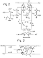
- Fig. 2 is a detailed circuit diagram representing the address buffer (ADD BUF) and the multiplexer (8) shown in F ig. 1. Since, in Fig. 1, the address buffers 7 1 through 7 n have the same construction and also the multiplexers 8 l through 8n have the same construction, only one of the address buffers 7 and only one of the multiplexers 8 are illustrated in Fig. 2.
- the multiplexer 8 receives, at its inputs, the external address ADD and the refresh address R, selectively, and the address buffer 7 produces the addresses A and A, according to the output of the multiplexer 8. It should be understood that the reference symbols ADD, R, a, A, A, 7 and 8 are respectively classified into each bit of address by using the sufixes 0 through n.
- the MOS transistor Q 31 is controlled, at its gate, by the clock PRF, so that if the external clock RFSH (Fig. 1) is changed to logic "H”, the'clock PRF is changed to logic "H”, and, thereby, the external clock ADD becomes effective.
- the MOS transistor Q 32 is controlled, at its gate, by the clock PRF so that if the external clock RFSH (Fig. 1) is changed to logic "L”,.the clock PRF is changed to logic "H”, and, thereby, the refresh address R supplied from the counter 3 (Fig. 1) becomes effective. Consequently, during the normal operation mode, logical conditions stand, that is RFSH is "H” and also PRF is "H".
- Fig. 3 is a timing diagram used for explaining the operation, especially the refresh operation, of the circuit shown in Fig. 2.
- the output from the reference clock generator 1 (Fig. 1) that is the clock PRF, changes from logic "H” to logic "L”, while the clock PRF changes from logic "L” to Logic "H”.
- the MOS transistor Q 32 is turned ON and, thereby, the input a is specified by the refresh address R.
- the timing diagram of Fig. 3 is depicted by taking, as an example, a case where the refresh address R has logic "H” and the external address ADD has logic "L".
- the address buffer 7 is comprised of MOS transistors Q 1 through Q 15 , as shown in Fig. 2.
- the MOS transistors Q through Q 5 comprise a flip.flop FF which functions as a main amplifier.
- the flip.flop FF includes nodes N 1 and N 2 which function as a pair of input terminals and a pair of output terminals of the flip ⁇ flop FF, alternatively.
- the node N 1 is provided with an external address input circuit IN 1 which is comprised of the MOS transistors Q 6 and Q 8 being connected in series.
- the node N 2 is provided with a reference voltage input circuit IN 2 which is comprised of the MOS transistors Q 7 and Q 9 being connected in series.
- the nodes N and N 2 are provided with an output circuit OUT which is comprised of the MOS transistors Q 10 through Q 15 .
- the output circuit OUT functions to pick up the amplified signal produced from the flip ⁇ flop (main amplifier) FF and produces the addresses A and A.
- the address buffer 7 is started by the application of the clock ⁇ 0 thereto. That is, when the clock ⁇ 0 starts rising, as shown by a curve ⁇ 0 in Fig. 3, the MOS transistors Q 6 and Q 8 are turned ON. In this case, the MOS transistor Q 9 is always maintained in a conductive state due to the presence of the reference voltage REF, at its gate. Accordingly, the level at the node N 2 is set to be a certain level which is determined by the ratio of the mutual conductances g m between the transistors Q 2 (depletion MOS transistor), Q 7 and Q 9' Generally, the value of the mutual conductance g m is determined by various factors, such as the size of the MOS transistor and voltage level applied to the gate thereof.
- the MOS transistor Q 8 to which the input a is applied, at its gate, is turned ON or OFF in accordance with logic "H” or "L” of the input a.
- the transistor Q is turned to ON, and, accordingly, a current flows through the MOS tran- s i s t ors Q1 (depletion MO S transistor), Q6 and Q 8 .
- the voltage level at the node N 1 is determined by the ratio of the mutual conductances g m defined by the respective transistors Q 1 , Q 6 and Q 8 .
- the value of g m defined by the transistor Q 8 is designed in advance to be larger than the value of g m defined by the aforementioned transistor Q 9 receiving the reference voltage RE F.
- the relationship V N1 ⁇ V N2 is obtained, where the symbols V N1 and V N2 denote the voltage levels developed at the nodes N 1 and N 2 , respectively.
- the input a is changed to logic "L”
- the relationship V N1 > V N2 is obtained, where the voltage V N1 is almost the same as the voltage level V CC (Figs. 2 and 3).
- V N1 ⁇ V N2 or the relationship V N1 > VN2 is created in accordance with the logic "H” or "L", respectively, of the input a.
- the difference between the voltages V N1 and V N2 is very small, and, therefore, the above recited two relationships are not remarkably distinguished from each other.
- the voltage levels V N1 and V N2 are amplified by the aforementioned flip-flop (main amplifier) FF.
- The-flip-flop FF is energized by the clock ⁇ 1 to be applied to the gate of the transistor Q 5 .
- the clock ⁇ 1 follows after the clock ⁇ 0 , as shown in Figs.
- the transistor Q 3 is turned OFF and, at the same time, the transistor Q 4 is turned ON.
- the voltage V N1 is reduced to the voltage level V SS and, at the same time, the voltage V N2 is increased to the voltage level V CC .
- a certain state is provided in which the voltage levels at both the nodes N 6 and N7 (corresponding to the drains of the transistors Q 10 and Q 11 , respectively) are precharged to a level of (V CC - V th ). Because, in this state, the voltage V CC is directly applied to the nodes N 1 and N 2 . Therefore, the transistors Q 10 and Q 11 are conductive, so that the nodes N 6 and N 7 are charged up with certain reduction of the voltage (threshold voltage V th of each of the transistors Q 10 and Q 11 ).
- the electric charges stored at the node N 7 are absorbed toward the node N 2 , now having the level V SS , via the conductive transistor Q 11 .
- the transistor Q 10 since the transistor Q 10 is nonconductive, the electric charges stored at the node N 6 remain as they are. Due to the presence of the electric charges at the node N 6 , the MOS transistor Q 12 is made fully conductive when the clock AD, having the level of V CC , is generated, because the so-called bootstrap effect is affected to the transistor Q 12 by the above-mentioned electric charges. Then the address A , having logic "H", is produced.
- the waveform of the clock AD is not shown in Fig. 3, but Figs. 6A and 6B.
- the generation of the clock ⁇ 0 should not be started until the logic level,of the input a from the multiplexer 8 is fully saturated to a predetermined level (refer to a time t 0 in Fig. 3).
- a waiting time should be created in the address buffer 7.
- the waiting time is indicated by the reference symbol t . This is the reason why the address buffer 7 of Fig. 2 may not operate sufficiently rapidly.
- the above-mentioned defect is derived from the existences of both the multiplexer 8 and the input circuit IN, shown in Fig. 2, which will be clarified hereinafter.
- An embodiment of the present invention can improve the operating speed of the memory, specifically to shorten the length of the above-mentioned waiting time t .
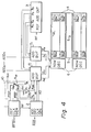
- Fig. 4 illustrates a circuit diagram of a dynamic memory which employs therein an address buffer and its neighboring members according to the present invention.
- members which are identical to those of Fig. 1 are represented by the same reference numerals and symbols. Therefore, members 10 and 17 1 through 17 n are newly employed in the memory of Fig. 4.
- members corresponding to the address buffer (ADD BUF) 17 1 through 17 n are illustrated in Fig. 1 as the address buffer 7 1 through 7 n .
- the member 10 is called a switcher.
- the switcher 10 switches the clock ⁇ 0 produced from the address drive clock generator 2 to a first signal path for transferring a clock ⁇ ON ; alternatively, the switcher 10 switches the clock ⁇ 0 to a second path for transferring a clock ⁇ OR .
- the refresh clock generator 1 produces the clock PRF having logic "H”, and, accordingly, the logic at node N 21 is changed to "H", via a MOS transistor Q 41 , which voltage level is equal to (V CC - V th ).
- the symbol V th is a threshold voltage of the transistor Q 41 .
- the clock ⁇ 0 is transferred, as the clock ⁇ ON , from the address drive clock generator 2 to the inputs of the address buffers 17 1 through 17 n via a MOS transistor Q 42 .
- the MOS transistor Q 41 is employed.
- the clock ⁇ 0 can be switched to the clock ⁇ ON or ⁇ OR only by using the gate transistors Q 42 and Q 44 controlled directly by the clocks PRF and P RF , where the voltage levels of the clocks ⁇ ON and ⁇ OR are lower than that of the clock ⁇ 0 .
- the so-called bootstrap effect is created in each of these combinations. In this case, the voltage levels at the nodes N 21 and N 22 are maintained at a level higher than the level V CC .
- the refresh clock generator 1 produces the clock PRF having logic "H", and, accordingly, the MOS transistor Q 44 is turned ON, so that the clock ⁇ 0 is transferred, as the clock ⁇ CR , to the inputs of the address buffers 17 1 through 17n.
- the clock ⁇ OR and the above-mentioned clock ⁇ ON are supplied alternatively from the switcher 10.
- the external address ADD 0 through ADD the refresh address R 0 through R or the inverting address R 0 through Rare selectively applied to the address buffers 17 1 through 17 n .
- Fig. 5 is a detailed circuit diagram representing the address buffer (ADD BUF) shown in Fig. 4.
- This circuit diagram corresponds to that of Fig. 2. Accordingly, members which are identical to those of Fig. 2 are represented by the same reference numerals and symbols. Since, in Fig. 4, the address buffers 17 1 through 17 n have the same construction as each other, only one of them is illustrated with the reference numeral 17. As compared with the cirucit diagram of Fig. 2, in Fig. 5, the external address input circuit (first input circuit) IN and also the reference voltage input circuit (second input circuit) IN 2 are still useful in the address buffer 17. However, the following three points should be noticed. First, the multiplexer 8, which is employed in the address buffer of F ig.
- the third input circuit IN 3 is connected, as a whole, in parallel with the first input circuit IN 1 .
- the circuit IN 3 receives the clock ⁇ OR and the refresh address R.
- the fourth input circuit IN 4 is connected, as a whole, in parallel with the second input circuit IN .
- the circuit IN receives the clock ⁇ OR and the inverted refresh address R.
- the first and second input circuits IN 1 and IN 2 are activated by the application of the clock ⁇ ON
- the third and fourth input circuits IN 3 and IN 4 are activated by the application of the clock ⁇ OR . That is, the MOS transistors Q 6 and Q 7 of the input circuits IN 1 and IN 2 are turned ON by the clock ⁇ ON during only the normal operation mode.
- the third input circuit IN 3 is comprised of MOS transistors Q 45 and Q47 connected in series, which MOS transistor Q 45 is turned ON by the clock ⁇ OR only during the refresh operation mode.
- the fourth input circuit IN 4 is comprised of MOS transistors Q 46 and Q 48 connected in series, which MOS transistor Q 46 is turned ON by the clock ⁇ OR only during the refresh operation mode.
- Fig. 6A is a timing diagram used for explaining the operation of the address buffer shown in Fig. 5, during the refresh operation mode.
- Fig. 6B is a timing diagram used for explaining the operation of the address buffer shown in F ig. 5, during the normal operation mode.
- the logic of the clock RFSH is changed from “H” to “L” and then the logic of the clock PRF is changed from “L” to “H” and, at the same time, the logic of the clock PRF is changed from “H” to “L” (these clocks PRF and PRF are produced from the refresh clock generator 1), which operations are identical to those represented in Fig. 3.
- Fig. 6A during the refresh operation mode, first the logic of the clock RFSH is changed from “H” to “L” and then the logic of the clock PRF is changed from “L” to “H” and, at the same time, the logic of the clock PRF is changed from “H” to “L” (these clocks PRF and PRF are produced from the refresh clock generator 1), which operations
- the clock ⁇ 0 and, accordingly, the clock ⁇ OR can be generated soon after the logic changes of the clocks PRF and PRF. In other words, it is not necessary to wait until the time the voltage level of the slow rising input a reaches its saturation level so as to generate the clock ⁇ 0 , as occurs in Fig. 3.
- the waiting time t w of Fig. 3 is considerably shortened to a waiting time t ' shown in Fig. 6A, and thereby a high speed operation of the address buffer can be expected.
- the reason why the input a can be removed from the address buffer 17 is that no member similar to the'multiplexer 8 of Fig. 2 is used, but, instead of such multiplexer 8, the third and fourth input circuits IN and IN 4 are employed in Fig. 5.
- the dynamic memory based on the present invention can operate with a high operating speed, as compared to that of Fig. 1.
- the characteristic curves N 21 , N22 ' PRF, PRF, R F and RFSH indicate the respective levels appearing in Fig. 4, but not in Fig. 5.
- the clocks RF, PRF, PRF may be activated approximately the same time as each other.
- the voltage level at the node N 22 can be increased over the level V CC , due to the previously mentioned bootstrap effect.
- the flip ⁇ flop FF is liable to be latched in either one of the two states, according to the logics of the refresh addresses R and R .
- the address R is set to be logic "H” and, accordingly, the address R is "L”
- the following relationship stands between the voltage levels V N1 at the node N 1 and V N2 at the node N 2 , that is V Nl ⁇ V N2 .
- the clock ⁇ 1 is applied from the clock generator 2 to the transistor Q 5 , at its gate, and the flip ⁇ flop FF is activated so as to make the transistors Q 3 and Q 4 ON and OFF, respectively.
- the output circuit OUT produces both the address A of logic "H” and the address A of logic L, simultaneously, so as to access the memory arrays 4.
Landscapes
- Engineering & Computer Science (AREA)
- Microelectronics & Electronic Packaging (AREA)
- Computer Hardware Design (AREA)
- Dram (AREA)
Applications Claiming Priority (2)
| Application Number | Priority Date | Filing Date | Title |
|---|---|---|---|
| JP31750/81 | 1981-03-05 | ||
| JP56031750A JPS57147193A (en) | 1981-03-05 | 1981-03-05 | Address buffer |
Publications (3)
| Publication Number | Publication Date |
|---|---|
| EP0060108A2 true EP0060108A2 (fr) | 1982-09-15 |
| EP0060108A3 EP0060108A3 (en) | 1985-09-18 |
| EP0060108B1 EP0060108B1 (fr) | 1988-08-17 |
Family
ID=12339691
Family Applications (1)
| Application Number | Title | Priority Date | Filing Date |
|---|---|---|---|
| EP82301141A Expired EP0060108B1 (fr) | 1981-03-05 | 1982-03-05 | Mémoire tampon d'adresse |
Country Status (5)
| Country | Link |
|---|---|
| US (1) | US4451908A (fr) |
| EP (1) | EP0060108B1 (fr) |
| JP (1) | JPS57147193A (fr) |
| DE (1) | DE3278924D1 (fr) |
| IE (1) | IE54166B1 (fr) |
Families Citing this family (7)
| Publication number | Priority date | Publication date | Assignee | Title |
|---|---|---|---|---|
| JPS60151893A (ja) * | 1984-01-18 | 1985-08-09 | Nec Corp | 半導体メモリ回路 |
| JPH0612614B2 (ja) * | 1986-06-06 | 1994-02-16 | 日本電気株式会社 | 半導体集積回路 |
| JPS63157397A (ja) * | 1986-12-22 | 1988-06-30 | Matsushita Electronics Corp | 半導体メモリ |
| JPH07101553B2 (ja) * | 1989-02-15 | 1995-11-01 | 三菱電機株式会社 | バッファ回路およびその動作方法 |
| JP2547268B2 (ja) * | 1990-03-14 | 1996-10-23 | シャープ株式会社 | 半導体記憶装置の内部アドレス決定装置 |
| KR100353544B1 (en) | 2000-12-27 | 2002-09-27 | Hynix Semiconductor Inc | Circuit for generating internal supply voltage of semiconductor memory device |
| KR100390238B1 (ko) | 2001-05-18 | 2003-07-07 | 주식회사 하이닉스반도체 | 뱅크 어드레스를 이용한 반도체 메모리 소자의 어드레스제어 장치 |
Family Cites Families (3)
| Publication number | Priority date | Publication date | Assignee | Title |
|---|---|---|---|---|
| US3737879A (en) * | 1972-01-05 | 1973-06-05 | Mos Technology Inc | Self-refreshing memory |
| US4207618A (en) * | 1978-06-26 | 1980-06-10 | Texas Instruments Incorporated | On-chip refresh for dynamic memory |
| WO1981003567A1 (fr) * | 1980-06-02 | 1981-12-10 | Mostek Corp | Memoire a semi-conducteur utilisee en association avec un circuit de detection et de correction d'erreurs |
-
1981
- 1981-03-05 JP JP56031750A patent/JPS57147193A/ja active Granted
-
1982
- 1982-03-03 US US06/354,499 patent/US4451908A/en not_active Expired - Lifetime
- 1982-03-04 IE IE492/82A patent/IE54166B1/en not_active IP Right Cessation
- 1982-03-05 EP EP82301141A patent/EP0060108B1/fr not_active Expired
- 1982-03-05 DE DE8282301141T patent/DE3278924D1/de not_active Expired
Also Published As
| Publication number | Publication date |
|---|---|
| IE54166B1 (en) | 1989-07-05 |
| EP0060108A3 (en) | 1985-09-18 |
| DE3278924D1 (en) | 1988-09-22 |
| JPH0146955B2 (fr) | 1989-10-11 |
| EP0060108B1 (fr) | 1988-08-17 |
| US4451908A (en) | 1984-05-29 |
| IE820492L (en) | 1982-09-05 |
| JPS57147193A (en) | 1982-09-10 |
Similar Documents
| Publication | Publication Date | Title |
|---|---|---|
| KR970008786B1 (ko) | 반도체 집적회로 | |
| US4568842A (en) | D-Latch circuit using CMOS transistors | |
| US4451745A (en) | Address buffer circuit with low power consumption | |
| US4316106A (en) | Dynamic ratioless circuitry for random logic applications | |
| US4514829A (en) | Word line decoder and driver circuits for high density semiconductor memory | |
| US4396845A (en) | Address buffer circuit | |
| KR100511356B1 (ko) | 반도체집적회로의구동방법및반도체집적회로 | |
| JPS6122495A (ja) | アドレス・バツフア回路 | |
| JPS633394B2 (fr) | ||
| JP3169987B2 (ja) | 入力緩衝回路を含む集積回路 | |
| US4894559A (en) | Buffer circuit operable with reduced power consumption | |
| EP0060108A2 (fr) | Mémoire tampon d'adresse | |
| US4797573A (en) | Output circuit with improved timing control circuit | |
| US4825420A (en) | C-MOS address buffer for semiconductor memory | |
| KR0155986B1 (ko) | 반도체 기억장치 | |
| US5199000A (en) | Semiconductor memory circuit having switched voltage supply for data bus lines | |
| US4446386A (en) | MOS Decoder circuit using phase clocking for reducing the power consumption | |
| JP3071408B2 (ja) | 半導体集積回路の駆動方法及び半導体集積回路 | |
| US6509772B1 (en) | Flip-flop circuit with transmission-gate sampling | |
| US3786277A (en) | Circuit arrangement of mos transistors operating according to the dynamic principle for decoding the addresses for an mos memory | |
| US4460983A (en) | Integrated dynamic read-write memory | |
| US4870620A (en) | Dynamic random access memory device with internal refresh | |
| US5600599A (en) | Data signal output circuit and semiconductor memory device including the same | |
| US4697108A (en) | Complementary input circuit with nonlinear front end and partially coupled latch | |
| JPH0580080B2 (fr) |
Legal Events
| Date | Code | Title | Description |
|---|---|---|---|
| PUAI | Public reference made under article 153(3) epc to a published international application that has entered the european phase |
Free format text: ORIGINAL CODE: 0009012 |
|
| AK | Designated contracting states |
Designated state(s): DE FR GB NL |
|
| PUAL | Search report despatched |
Free format text: ORIGINAL CODE: 0009013 |
|
| AK | Designated contracting states |
Designated state(s): DE FR GB NL |
|
| 17P | Request for examination filed |
Effective date: 19851213 |
|
| 17Q | First examination report despatched |
Effective date: 19870126 |
|
| GRAA | (expected) grant |
Free format text: ORIGINAL CODE: 0009210 |
|
| AK | Designated contracting states |
Kind code of ref document: B1 Designated state(s): DE FR GB NL |
|
| PG25 | Lapsed in a contracting state [announced via postgrant information from national office to epo] |
Ref country code: NL Effective date: 19880817 |
|
| REF | Corresponds to: |
Ref document number: 3278924 Country of ref document: DE Date of ref document: 19880922 |
|
| ET | Fr: translation filed | ||
| NLV1 | Nl: lapsed or annulled due to failure to fulfill the requirements of art. 29p and 29m of the patents act | ||
| PLBE | No opposition filed within time limit |
Free format text: ORIGINAL CODE: 0009261 |
|
| STAA | Information on the status of an ep patent application or granted ep patent |
Free format text: STATUS: NO OPPOSITION FILED WITHIN TIME LIMIT |
|
| 26N | No opposition filed | ||
| PGFP | Annual fee paid to national office [announced via postgrant information from national office to epo] |
Ref country code: GB Payment date: 19980224 Year of fee payment: 17 |
|
| PGFP | Annual fee paid to national office [announced via postgrant information from national office to epo] |
Ref country code: FR Payment date: 19980310 Year of fee payment: 17 |
|
| PGFP | Annual fee paid to national office [announced via postgrant information from national office to epo] |
Ref country code: DE Payment date: 19980313 Year of fee payment: 17 |
|
| PG25 | Lapsed in a contracting state [announced via postgrant information from national office to epo] |
Ref country code: GB Free format text: LAPSE BECAUSE OF NON-PAYMENT OF DUE FEES Effective date: 19990305 |
|
| GBPC | Gb: european patent ceased through non-payment of renewal fee |
Effective date: 19990305 |
|
| PG25 | Lapsed in a contracting state [announced via postgrant information from national office to epo] |
Ref country code: FR Free format text: LAPSE BECAUSE OF NON-PAYMENT OF DUE FEES Effective date: 19991130 |
|
| REG | Reference to a national code |
Ref country code: FR Ref legal event code: ST |
|
| PG25 | Lapsed in a contracting state [announced via postgrant information from national office to epo] |
Ref country code: DE Free format text: LAPSE BECAUSE OF NON-PAYMENT OF DUE FEES Effective date: 20000101 |