EP0060343A2 - Convertisseur de tension - Google Patents
Convertisseur de tension Download PDFInfo
- Publication number
- EP0060343A2 EP0060343A2 EP81110192A EP81110192A EP0060343A2 EP 0060343 A2 EP0060343 A2 EP 0060343A2 EP 81110192 A EP81110192 A EP 81110192A EP 81110192 A EP81110192 A EP 81110192A EP 0060343 A2 EP0060343 A2 EP 0060343A2
- Authority
- EP
- European Patent Office
- Prior art keywords
- voltage
- converter
- output
- comparator
- regulator
- Prior art date
- Legal status (The legal status is an assumption and is not a legal conclusion. Google has not performed a legal analysis and makes no representation as to the accuracy of the status listed.)
- Granted
Links
- 108010076504 Protein Sorting Signals Proteins 0.000 claims abstract description 8
- 230000001419 dependent effect Effects 0.000 claims abstract 2
- 239000003990 capacitor Substances 0.000 claims description 34
- 238000004804 winding Methods 0.000 description 4
- 230000002349 favourable effect Effects 0.000 description 3
- 230000001629 suppression Effects 0.000 description 3
- 238000010586 diagram Methods 0.000 description 2
- 238000001816 cooling Methods 0.000 description 1
- 230000007547 defect Effects 0.000 description 1
- 238000011161 development Methods 0.000 description 1
- 230000018109 developmental process Effects 0.000 description 1
- 238000009413 insulation Methods 0.000 description 1
- 230000010354 integration Effects 0.000 description 1
- 238000001208 nuclear magnetic resonance pulse sequence Methods 0.000 description 1
- 230000001105 regulatory effect Effects 0.000 description 1
- 230000000630 rising effect Effects 0.000 description 1
Images

Classifications
-
- H—ELECTRICITY
- H02—GENERATION; CONVERSION OR DISTRIBUTION OF ELECTRIC POWER
- H02M—APPARATUS FOR CONVERSION BETWEEN AC AND AC, BETWEEN AC AND DC, OR BETWEEN DC AND DC, AND FOR USE WITH MAINS OR SIMILAR POWER SUPPLY SYSTEMS; CONVERSION OF DC OR AC INPUT POWER INTO SURGE OUTPUT POWER; CONTROL OR REGULATION THEREOF
- H02M3/00—Conversion of DC power input into DC power output
- H02M3/22—Conversion of DC power input into DC power output with intermediate conversion into AC
- H02M3/24—Conversion of DC power input into DC power output with intermediate conversion into AC by static converters
- H02M3/28—Conversion of DC power input into DC power output with intermediate conversion into AC by static converters using discharge tubes with control electrode or semiconductor devices with control electrode to produce the intermediate AC
- H02M3/325—Conversion of DC power input into DC power output with intermediate conversion into AC by static converters using discharge tubes with control electrode or semiconductor devices with control electrode to produce the intermediate AC using devices of a triode or a transistor type requiring continuous application of a control signal
- H02M3/335—Conversion of DC power input into DC power output with intermediate conversion into AC by static converters using discharge tubes with control electrode or semiconductor devices with control electrode to produce the intermediate AC using devices of a triode or a transistor type requiring continuous application of a control signal using semiconductor devices only
- H02M3/33507—Conversion of DC power input into DC power output with intermediate conversion into AC by static converters using discharge tubes with control electrode or semiconductor devices with control electrode to produce the intermediate AC using devices of a triode or a transistor type requiring continuous application of a control signal using semiconductor devices only with automatic control of the output voltage or current, e.g. flyback converters
Definitions
- the invention relates to a voltage converter with a converter transformer and a voltage regulator according to the preamble of the main claim.
- a voltage converter is already known from the magazine "Markt undtechnik", No. 37, September 1980, page 68.
- voltage transformers When using voltage transformers to supply electronic safety devices as well as medical and military electronic devices, in which a failure of the voltage supply would have particularly serious consequences, voltage fluctuations, falling input voltages down to very low values and interference voltages must have no or only a very slight influence on the voltage supply of the power supplying electronic device. Intervention of various additional security measures should be simple and inexpensive to implement.
- the voltage converter according to the invention with the characterizing features of the main claim has the advantage that it works as a very safe system down to very low input voltage values and is very insensitive to interference. Intervention of a wide variety of safety and control measures is possible in a simple and inexpensive manner on the output voltage of the voltage regulator contained in the control loop.
- the measures listed in the subclaims allow advantageous developments and improvements of the voltage converter specified in the main claim. It is particularly advantageous to limit the output voltage of the voltage regulator by means of a voltage divider, the tap of which is connected both to the output of the voltage regulator and to ground via a storage capacitor. In this way, the maximum pulse duration for the primary-side control of the converter transformer can be limited, as a result of which the corresponding control transistor is protected against overload, which represents a further contribution to the safety of the overall system.
- a second comparator for comparing the output voltage of the voltage converter with its supply voltage, the output voltage of the voltage regulator at the input of the first comparator being able to be reduced when the output voltage of the voltage converter drops below the supply voltage.
- protection of the voltage converter in the event of a short-circuit on the output side and a switch-on delay are achieved if, for example, when the electronic device to be supplied is switched on, a relatively slow voltage build-up initially takes place. This is particularly the case when capacitors as energy reserves of a safety device first have to be charged. If the converter would have to deliver the necessary current immediately, the output stage would be overloaded, or it would have to be dimensioned in a more complex manner, and a capacity control of the capacitors of the energy reserve by the safety device would not be possible.
- the output signal sequence of the first comparator to the converter transformer via a three-stage transistor arrangement which consists of an npn, a pnp and an npn transistor, the emitter of the pnp transistor being connected directly to the supply voltage.
- the output stage npn transistor remains controllable down to the lowest supply voltages.
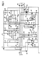
- FIG. 1 shows a circuit configuration of the exemplary embodiment
- FIG. 2 shows a signal diagram for explaining the converter clock generation.
- a terminal 10 connected to the positive pole of the supply voltage is connected to ground via the series connection of a diode 11 with a capacitor 12.
- a resistor 13 with a Zener diode 14 is connected in series with the capacitor 12.
- the voltage across the Zener diode 14 is supplied to a PI controller 15 as the desired voltage.
- the output voltage of the voltage converter connected to a terminal 16 is connected to ground via a voltage divider consisting of two resistors 17, 18.
- the tap between the two resistors 17, 18 is fed to the actual voltage input of the PI controller 15 via a further resistor 19.
- the resistor 18 is designed as a variable resistor in order to be able to set the desired output voltage of the voltage regulator.
- the PI controller 15 consists of a circuit known per se from a comparator 20, which has negative feedback from two branches connected in parallel, a capacitor 21 being connected in the first branch and the series connection of a capacitor 22 connected to a resistor 23 in the second branch is.
- the PI controller 15 uses a resistor 24 as the load resistor and a capacitor 26 as the integration element.
- the output voltage of the comparator 20 is connected to the tap of a voltage divider consisting of two resistors 24, 25, which is connected in parallel to the capacitor 12.
- a capacitor 26 for storing the output voltage of the comparator 20 is connected in parallel with the resistor 25 designed as a variable resistor.
- the voltage applied to the capacitor 26 is fed to the non-inverting input of a comparator 29 via the parallel connection of a resistor 27 with a diode 28.
- the output voltage of a delta voltage generator 30 is applied to the inverting input of this comparator 29.
- This delta voltage generator consists, in a manner known per se, of a comparator 31, which is also coupled via a resistor 32 and is negatively coupled via a resistor 33.
- the tap voltage of a voltage divider consisting of two resistors 35, 36 is connected to the non-inverting input of the comparator 31 and is connected in parallel to the capacitor 12.
- the voltage applied to the capacitor 12 is also connected via a resistor 37 to the output of the comparator 29 and via a resistor 38 to the output of the comparator 31.
- the output of this comparator 31 is connected via a capacitor 39 to the non-inverting input of the comparator 29.
- the output of the comparator 29 is connected to the base of a first npn transistor 40 which, together with a pnp transistor 41 and a second npn transistor 42, represents a three-stage transistor arrangement. It is the base of transistor 41 is connected to a resistor 44 via the series connection of a diode 43 and the collector-emitter path of transistor 40 is connected to ground. The emitter of transistor 41 connected to terminal 10 is connected to its base via a resistor 45. The collector of transistor 41 is connected via the series circuit of a resistor 46 with an inductance 47 to the base of transistor 42 connected as an output stage transistor. A resistor 48 is connected between the base and the emitter of transistor 42.
- the series connection of the primary winding of a converter transformer 49 with the collector-emitter path of the transistor 42 and a polarity reversal protection diode 50 is connected between the terminal 10 and ground.
- a capacitor 51 is connected between the emitter of transistor 42 and terminal 10. Due to the arrangement described, a press-in diode can be used as the polarity reversal protection diode 50, which may be connected to the ground potential without insulation measures on the cathode side and thus with the cooling plate.
- press-in diodes are, on the one hand, easy to install and are cheaply available as mass-produced diodes for high currents.
- a Zener diode 52 is connected between the base of transistor 41 and the emitter of transistor 42.
- the series connection of a diode 53 with a capacitor 54 is connected in parallel with the secondary winding of the converter transformer 49.
- the connection of the capacitor 54 facing away from the diode is connected to ground.
- the capacitor voltage of the capacitor 54 is connected on the one hand via a diode 55 to the output terminal 16 and on the other hand via a diode 56 to the cathode of the diode 11. In this way, the voltage across the capacitor 12 and thus the supply voltage for the components 13 to 39 are passed through determines the higher of the two voltages at terminals 10 and 16. This serves for additional security of the overall system.
- a voltage divider consisting of two resistors 57, 58 is connected in parallel with capacitor 12, the tap of which is fed to the inverting input of a comparator 59.
- Another voltage divider consisting of two resistors 60, 61 is connected between terminal 16 and ground. The tap of this voltage divider is connected to the non-inverting input of the comparator 59, the output of which is connected to the non-inverting input of the comparator 29.
- a Zener diode 62 is connected between the cathode of the diode 53 and the inverting input of the comparator 59.
- a control device designed as a control lamp 63 for checking the proper functioning of the voltage converter, a resistor 64, the collector-emitter path of a transistor 65 and the polarity reversal protection diode 50 form a series circuit connected between the terminal 10 and ground.
- the collector-emitter path of a transistor 66 is connected in parallel to the base-emitter path of the transistor 65, the collector of which is connected to the terminal 10 via a resistor 67.
- a resistor 68 is connected in parallel with the capacitor 54, the voltage drop of which is supplied to the base of the transistor 66 via a resistor 69.
- the mode of operation of the exemplary embodiment shown in FIG. 1 will be explained below with the aid of the signal diagram shown in FIG. 2.
- the PI controller 15 generates an output signal as a function of the difference between the nominal voltage applied to the Zener diode 14 and the divided actual voltage applied to the variable resistor 18, that is to say divided output voltage of the voltage converter.
- the capacitor 26 specifies the comparison voltage at the non-inverting input of the comparator 29.
- the output voltage of the PI controller can be limited to the division ratio of the resistors 24, 25.
- This voltage limitation acts as a limitation of the maximum pulse duration of the output signal sequence of the comparator 29 and thus serves to protect the transistor 42 connected as an output stage transistor. It is thereby prevented that the pulse duration of the output pulse sequence of the comparator 29 becomes too long when switched on and when the output current is excessive.
- the comparator 29 compares the voltage U15 with the delta voltage U30 of the delta voltage generator 30. An output signal U29 is only generated when the delta voltage U30 is below the voltage U15.
- a constant emergency operation of the voltage converter is maintained via the capacitor 39, which ensures that when the supply voltage rises, the output voltage of the voltage converter does not break down. By one at a time. Edge of the rectangular signal sequence at the output of the comparator 31, a short pulse is given to the non-inverting input of the comparator 29 via this capacitor 39. During this short pulse, there is a short current surge through the primary winding of the converter transformer 49, which prevents a reduction in the voltage of the capacitor voltage 54. The diode 28 serves to charge the capacitor 39.
- the signal sequence U29 is amplified via the three transistors 40 to 42, as a result of which corresponding current flow times are generated in the primary winding of the converter transformer 49. This absorbs the corresponding magnetic energy and delivers it to the capacitor 54 via the diode 53 until the next signal, which increases its voltage. This voltage is in turn regulated via the control loop described.
- the three-stage transistor arrangement 40 to 42 is formed by the npn-pnp-npn sequence so that the voltage converter still works down to very low supply voltages. This is ensured above all by the fact that the emitter of transistor 41 is connected directly to the supply voltage.
- the dynamic voltage drop at the input transistor 40 can also be used for driving.
- the resistor 46 can be designed to have a very low resistance (for example 1.5 ohms), since the base current through the inductor 47 is limited at high supply voltages and correspondingly short control signals becomes, while at low battery voltages and correspondingly long control signals, the influence of this inductance 47 is negligible.
- a diode 70 connected in parallel with the inductance 47 serves as a freewheeling diode.
- the diode 43 serves to block negative interference pulses, while the Z diode 52 excludes positive interference pulses which are above the Z voltage.
- the circuit arrangement of components 57 to 61 has two tasks: suppression of the converter function during the start-up phase and protection in the event of a short circuit in the output.
- the effective supply voltage on capacitor 12 is compared with the output voltage of the voltage converter at terminal 16 by the two voltage dividers 57, 58 and 60 61. Both during the start-up phase and in the event of a short circuit, a lower voltage value is present at terminal 16, which means that the comparator 59 goes to zero potential on the output side. This zero potential also pulls the non-inverting input of the comparator 29 to a zero potential, as a result of which the signal sequence U29 is suppressed.
- This suppression during the start-up phase serves, on the one hand, to protect the voltage converter under high load and, in the case of supplying a capacitive energy reserve by the voltage converter, e.g. in a safety device according to DE-PS 22 32 179, the checking of this energy reserve for correct function after switching on this safety device.
- the voltage converter thus has no influence on this check and realizes a "soft start” after suppression of the converter function by charging capacitor 26.
- the Z diode 62 limits the output voltage of the voltage converter, that is to say the voltage across the capacitor 54, in a simple manner. If the voltage rises above the limit value, the Zener diode 62 breaks down and, according to the above statements, pulls the non-inverting input of the comparator 29 to zero potential.
- Components 63 to 69 monitor the converter function.
- the transistor 66 If the voltage across the capacitor 54 is above a minimum permissible voltage, the transistor 66 is conductive and, accordingly, the transistor 65 is blocked. The indicator lamp 63 does not light up. If the output voltage falls below this minimum value, both transistors 65, 66 reverse and the indicator lamp 63 lights up, which indicates an error.
- the four comparators can preferably be implemented by a 4-way comparator available as an integrated circuit.
Landscapes
- Engineering & Computer Science (AREA)
- Power Engineering (AREA)
- Dc-Dc Converters (AREA)
Applications Claiming Priority (2)
| Application Number | Priority Date | Filing Date | Title |
|---|---|---|---|
| DE3109612 | 1981-03-13 | ||
| DE19813109612 DE3109612A1 (de) | 1981-03-13 | 1981-03-13 | Spannungswandler |
Publications (3)
| Publication Number | Publication Date |
|---|---|
| EP0060343A2 true EP0060343A2 (fr) | 1982-09-22 |
| EP0060343A3 EP0060343A3 (en) | 1983-06-22 |
| EP0060343B1 EP0060343B1 (fr) | 1985-07-31 |
Family
ID=6127118
Family Applications (1)
| Application Number | Title | Priority Date | Filing Date |
|---|---|---|---|
| EP81110192A Expired EP0060343B1 (fr) | 1981-03-13 | 1981-12-05 | Convertisseur de tension |
Country Status (3)
| Country | Link |
|---|---|
| US (1) | US4439820A (fr) |
| EP (1) | EP0060343B1 (fr) |
| DE (2) | DE3109612A1 (fr) |
Families Citing this family (5)
| Publication number | Priority date | Publication date | Assignee | Title |
|---|---|---|---|---|
| DE3336422A1 (de) * | 1983-10-06 | 1985-04-18 | Siemens AG, 1000 Berlin und 8000 München | Sperrwandler-schaltnetzteil |
| US4929872A (en) * | 1988-01-11 | 1990-05-29 | Eastman Kodak Company | Light bulb socket soft start and power interrupt assembly |
| US4809150A (en) * | 1988-01-27 | 1989-02-28 | Electric Power Research Institute, Inc. | DC to DC converter with feed forward and feed back regulation |
| DE4126544A1 (de) * | 1991-08-10 | 1993-02-11 | Dresden Messelektronik Gmbh | Stabilisierender elektronischer halbwellenconverter fuer ohmsche verbraucher mit diskreter oder breitbandiger hochfrequenter energieuebertragung |
| EP3349090A4 (fr) * | 2015-09-09 | 2019-06-12 | Closed-up Joint-Stock Company Drive | Dispositif pour générer de la tension électrique continue (et variantes) |
Family Cites Families (11)
| Publication number | Priority date | Publication date | Assignee | Title |
|---|---|---|---|---|
| US3569818A (en) * | 1969-07-22 | 1971-03-09 | Hughes Aircraft Co | Multiple output dc voltage regulator |
| FR2063511A5 (fr) * | 1969-10-20 | 1971-07-09 | Sautel Auguste | |
| US3670234A (en) * | 1970-06-30 | 1972-06-13 | Ibm | Pulse width modulated voltage regulator |
| US3953779A (en) * | 1974-05-30 | 1976-04-27 | Francisc Carol Schwarz | Electronic control system for efficient transfer of power through resonant circuits |
| DE2445033C3 (de) * | 1974-09-20 | 1978-05-03 | Siemens Ag, 1000 Berlin Und 8000 Muenchen | Gleichstromumrichter |
| JPS5283127A (en) * | 1975-12-31 | 1977-07-11 | Fujitsu Ltd | Instantaneous power cut detecting circuit |
| US4071884A (en) * | 1976-06-14 | 1978-01-31 | Micro Components Corporation | Integrated circuit high voltage DC converter |
| JPS5529234A (en) * | 1978-08-17 | 1980-03-01 | Matsushita Electric Ind Co Ltd | Power supply device |
| JPS5583463A (en) * | 1978-12-13 | 1980-06-23 | Matsushita Electric Ind Co Ltd | Power supply |
| JPS5854743B2 (ja) * | 1979-01-20 | 1983-12-06 | 横河電機株式会社 | スイッチング・レギュレ−タ |
| US4301497A (en) * | 1980-06-16 | 1981-11-17 | International Business Machines Corporation | Flyback converter control with feed forward |
-
1981
- 1981-03-13 DE DE19813109612 patent/DE3109612A1/de not_active Withdrawn
- 1981-12-05 DE DE8181110192T patent/DE3171621D1/de not_active Expired
- 1981-12-05 EP EP81110192A patent/EP0060343B1/fr not_active Expired
-
1982
- 1982-01-28 US US06/343,405 patent/US4439820A/en not_active Expired - Fee Related
Also Published As
| Publication number | Publication date |
|---|---|
| US4439820A (en) | 1984-03-27 |
| EP0060343B1 (fr) | 1985-07-31 |
| DE3109612A1 (de) | 1982-09-23 |
| EP0060343A3 (en) | 1983-06-22 |
| DE3171621D1 (en) | 1985-09-05 |
Similar Documents
| Publication | Publication Date | Title |
|---|---|---|
| DE2124579A1 (de) | Schaltung zum automatischen Aufladen einer Batterie | |
| DE1053591B (de) | Schutzschaltung zur Vermeidung der UEberlastung eines Oszillators, dessen Schwingungen hochtransformiert und danach gleichgerichtet werden | |
| DE3713540A1 (de) | Kombinierter sekundaerschalter | |
| DE3335153C2 (fr) | ||
| DE2554058C3 (de) | Schaltungsanordnung zum Umwandeln einer Eingangs-Gleichspannung in eine nahezu konstante Ausgangsgleichspannung | |
| DE3537920C2 (de) | Stabilisator mit Schutz gegen Übergangs-Überspannungen, deren Polarität entgegengesetzt zur Polarität des Generators ist, insbesondere für die Verwendung in Kraftfahrzeugen | |
| DE2114284A1 (de) | Selbstregulierter Gleichstrom-Gleichstrom-Konverter | |
| EP0060343B1 (fr) | Convertisseur de tension | |
| EP0339598A2 (fr) | Circuit de protection pour charges inductives | |
| DE2110427A1 (de) | Schaltungsanordnung zur Abgabe einer bestimmten Ausgangsspannung auf die Aufnahme einer Eingangsspannung hin | |
| DE3822021C1 (fr) | ||
| DE2605626A1 (de) | Wandler zur erzeugung eines elektrischen ausgangssignales in abhaengigkeit von einem mechanischen eingangssignal | |
| DE2043594A1 (de) | Spannungsw andler | |
| EP0737379A1 (fr) | Transformateur de tension | |
| DE2239796A1 (de) | Auf einen ueberspannungszustand ansprechende anordnung zur erzeugung eines frequenzerhoehungs-steuersignales | |
| EP0266743A2 (fr) | Disposition de circuit pour produire une tension d'alimentation interne dans une alimentation de courant à découpage | |
| DE2621471C3 (de) | Schaltung zur Regelung der Ausgangsspannungen einer Kommutatorablenkschaltung | |
| DE69108188T2 (de) | Regelungsvorrichtung für die, von einem Wechselstromgenerator abgegebene, Batteriespannung. | |
| EP0987806A2 (fr) | Circuit d'interruption en cas de surtension | |
| DE10260321B4 (de) | Schaltungsanordnung zur Funkentstörung einer Kraftfahrzeugzündanlage | |
| DE3918134C2 (de) | Getaktete stromversorgungseinrichtung | |
| DE3000324C2 (de) | Sicherheitsschaltung für einen Spannungsregler | |
| DE3440888A1 (de) | Spannungskonstanthalter zur stromversorgung elektronischer steuergeraete | |
| DE1613030C (de) | Gleichspannungswandler | |
| DE2843255A1 (de) | Batterieladesystem |
Legal Events
| Date | Code | Title | Description |
|---|---|---|---|
| PUAI | Public reference made under article 153(3) epc to a published international application that has entered the european phase |
Free format text: ORIGINAL CODE: 0009012 |
|
| 17P | Request for examination filed |
Effective date: 19811205 |
|
| AK | Designated contracting states |
Designated state(s): DE FR GB IT SE |
|
| PUAL | Search report despatched |
Free format text: ORIGINAL CODE: 0009013 |
|
| RHK1 | Main classification (correction) |
Ipc: H02M 3/335 |
|
| AK | Designated contracting states |
Designated state(s): DE FR GB IT SE |
|
| ITF | It: translation for a ep patent filed | ||
| GRAA | (expected) grant |
Free format text: ORIGINAL CODE: 0009210 |
|
| AK | Designated contracting states |
Designated state(s): DE FR GB IT SE |
|
| REF | Corresponds to: |
Ref document number: 3171621 Country of ref document: DE Date of ref document: 19850905 |
|
| ET | Fr: translation filed | ||
| PLBE | No opposition filed within time limit |
Free format text: ORIGINAL CODE: 0009261 |
|
| STAA | Information on the status of an ep patent application or granted ep patent |
Free format text: STATUS: NO OPPOSITION FILED WITHIN TIME LIMIT |
|
| 26N | No opposition filed | ||
| GBPC | Gb: european patent ceased through non-payment of renewal fee | ||
| PG25 | Lapsed in a contracting state [announced via postgrant information from national office to epo] |
Ref country code: GB Free format text: LAPSE BECAUSE OF NON-PAYMENT OF DUE FEES Effective date: 19881121 |
|
| REG | Reference to a national code |
Ref country code: FR Ref legal event code: DL |
|
| PGFP | Annual fee paid to national office [announced via postgrant information from national office to epo] |
Ref country code: SE Payment date: 19920228 Year of fee payment: 11 |
|
| PGFP | Annual fee paid to national office [announced via postgrant information from national office to epo] |
Ref country code: FR Payment date: 19920514 Year of fee payment: 11 |
|
| PG25 | Lapsed in a contracting state [announced via postgrant information from national office to epo] |
Ref country code: SE Effective date: 19921206 |
|
| PGFP | Annual fee paid to national office [announced via postgrant information from national office to epo] |
Ref country code: DE Payment date: 19930301 Year of fee payment: 12 |
|
| PG25 | Lapsed in a contracting state [announced via postgrant information from national office to epo] |
Ref country code: FR Effective date: 19930831 |
|
| REG | Reference to a national code |
Ref country code: FR Ref legal event code: ST |
|
| PG25 | Lapsed in a contracting state [announced via postgrant information from national office to epo] |
Ref country code: DE Effective date: 19940901 |
|
| EUG | Se: european patent has lapsed |
Ref document number: 81110192.2 Effective date: 19930709 |