EP0060427A2 - Elément sensible pour la mesure de dimensions physiques ainsi que procédé pour sa fabrication et son utilisation - Google Patents
Elément sensible pour la mesure de dimensions physiques ainsi que procédé pour sa fabrication et son utilisation Download PDFInfo
- Publication number
- EP0060427A2 EP0060427A2 EP82101524A EP82101524A EP0060427A2 EP 0060427 A2 EP0060427 A2 EP 0060427A2 EP 82101524 A EP82101524 A EP 82101524A EP 82101524 A EP82101524 A EP 82101524A EP 0060427 A2 EP0060427 A2 EP 0060427A2
- Authority
- EP
- European Patent Office
- Prior art keywords
- sensor
- layer
- sensor according
- measuring
- substrate
- Prior art date
- Legal status (The legal status is an assumption and is not a legal conclusion. Google has not performed a legal analysis and makes no representation as to the accuracy of the status listed.)
- Granted
Links
Images


Classifications
-
- G—PHYSICS
- G01—MEASURING; TESTING
- G01K—MEASURING TEMPERATURE; MEASURING QUANTITY OF HEAT; THERMALLY-SENSITIVE ELEMENTS NOT OTHERWISE PROVIDED FOR
- G01K7/00—Measuring temperature based on the use of electric or magnetic elements directly sensitive to heat ; Power supply therefor, e.g. using thermoelectric elements
- G01K7/16—Measuring temperature based on the use of electric or magnetic elements directly sensitive to heat ; Power supply therefor, e.g. using thermoelectric elements using resistive elements
- G01K7/22—Measuring temperature based on the use of electric or magnetic elements directly sensitive to heat ; Power supply therefor, e.g. using thermoelectric elements using resistive elements the element being a non-linear resistance, e.g. thermistor
- G01K7/223—Measuring temperature based on the use of electric or magnetic elements directly sensitive to heat ; Power supply therefor, e.g. using thermoelectric elements using resistive elements the element being a non-linear resistance, e.g. thermistor characterised by the shape of the resistive element
-
- G—PHYSICS
- G01—MEASURING; TESTING
- G01K—MEASURING TEMPERATURE; MEASURING QUANTITY OF HEAT; THERMALLY-SENSITIVE ELEMENTS NOT OTHERWISE PROVIDED FOR
- G01K13/00—Thermometers specially adapted for specific purposes
- G01K13/20—Clinical contact thermometers for use with humans or animals
Definitions
- the invention relates to a sensor for measuring physical quantities as well as a method for its production and its use.
- Sensors for measuring physical quantities are known in various forms. They are used, for example, to determine temperature, pressure, flow, Magnetic field, light exposure and other sizes.
- the calibration consistency and the service life quality also change over time.
- the manufacturing tolerances are often large, with a correspondingly negative influence on the measurement accuracy and thus the resulting lack of reproducibility of measurement results when changing the sensor element.
- the invention has for its object to design the sensor of the type mentioned in such a way that an accurate measurement result can be achieved very quickly while avoiding the disadvantages shown.
- the sensor should have a high quality of life and should be able to be manufactured in a relatively simple and inexpensive manner.
- the invention there are geometrically predetermined doped Be on a poorly conductive, flat substrate rich in polycrystalline silicon, which are in contact with conductor tracks that lead to the outside.
- Polycrystalline silicon has the property that its crystallographic structure can only change at high temperatures of about 500 ° C. This means that the crystal structure once set remains practically unchanged at low temperatures.
- the construction of the sensor according to the invention thus ensures a long service life and calibration accuracy.
- important material properties such as resistance and temperature coefficient can be continuously changed over a wide range.
- Specified physical parameters can be achieved with high accuracy using a specific setting procedure.
- the doped component is exposed to intensive radiation and the change occurring within the component is measured, the measurement result being used to control the radiation intensity and duration.
- the component is embedded in a system for generating predetermined environmental conditions. Ambient conditions within the system can be a certain temperature, pressure, bending, flow, light irradiation, humidity, and / or other conditions.
- Quartz is preferably used as the poorly conductive, flat substrate. In addition to excellent insulation properties, quartz has an extremely low thermal conductivity. The test specimen is only negligibly cooled due to the low heat capacity of the sensor and a negligible heat dissipation through the quartz substrate, so that an extremely high measuring accuracy results in particular in the case of heat measurements.
- the planar structure of the sensor on the flat substrate enables one when using monocrystalline sili Design that is difficult to implement and does not require wire bonding. In this way, easy physical access to the sensor can be achieved, ie the sensor can always be brought in close proximity to the object or the environment whose physical state is to be measured. Due to the direct accessibility of the sensor, a quick measurement result can be achieved. The less complicated and robust construction ensures little mechanical influence and thus a long service life.
- the layer thickness of the polycrystalline silicon is preferably 0.5 ⁇ m, with the geometrically predetermined doped region preferably having the shape of a van der Pauw figure.
- van der Pauw figures as a measuring figure, a slight dependence of the displayed value on the geometric shape of the measuring figure is guaranteed.
- the manufacturing spread is less severe than with other measuring figures.
- the senor is coated with a quartz layer, a silicon nitride layer or a protective lacquer.
- the ends of the conductor tracks led to the outside at the edge of the substrate can be galvanically thickened, so that the sensor can be contacted by inserting it into a standard plug. Future contact strips can also be soldered to the conductor tracks. Finally, gold wire bonding to the conductor tracks is also possible, as well as other forms of bonding (bondinq).
- At least one of the contacts of the polycrystalline measurement figure can be connected from the back of the substrate.
- the sensor according to the invention can be manufactured much more cost-effectively because a larger number of sensors can be manufactured per manufactured area because of the smaller area requirement of the individual sensor.
- the measuring figure is bipolar.
- the substrate is preferably located as a layer on a low-ohmic carrier substrate, via which the backside contact is made through an opening in the substrate layer.
- a second SiO 2 layer is applied to the substrate layer consisting of Sio 2 , which covers the sensor measurement figure and has an opening for the front-side contact.
- the front of the sensor is expediently metallized, in order to avoid short circuits, the metallization of the front can also be structured, wherein an electrical connection of the metallization to the front contact is made via an opening in the second layer that overcomes the measurement, while the rear of the carrier substrate is also q is metallized over the entire surface.
- the metallization consists of an approximately 1.5 ⁇ m thick aluminum layer.
- the method according to the invention for producing the sensor is characterized in that a layer of polycrystalline silicon in the form of a predetermined geometric figure is applied to a poorly conductive, flat substrate, a doping is introduced into the figure, conductor tracks which lead to the outside are applied to the silicon layer and covers the sensor with a passivation layer.
- the polycrystalline silicon layer is preferably applied to the substrate, which preferably consists of quartz or oxidized silicon, using the chemical vapor deposition method, vapor deposition or sputtering. With the aid of known lithographic processes, resistance or van der Pauw figures are produced in this layer in such a way that only the figures remain on the substrate while the silicon regions in between are etched away. Then the contact areas of the resistance or van der Pauw figures are heavily predoped using a lithography and a doping process (sheet resistance ⁇ 30 ⁇ ).
- a doping with a typical sheet resistance of about ⁇ 500 ⁇ is first introduced.
- heat treatment takes place in a diffusion furnace, the treatment temperature preferably being between approximately 900 and approximately 1100 ° C., or irradiation with a laser for recrystallization of the polycrystalline structure, the radiation conditions depending on the laser type and the structure of the steel on the other hand irradiation also takes place by means of an electron beam.
- Predefined sheet resistances or other physical parameters can be set by means of a trimming apparatus, in which the properties of the polycrystalline silicon are changed by laser irradiation. The change is controlled by simultaneous measurement of the electrical properties and control electronics.
- the component is preferably embedded in a system for generating predetermined environmental conditions.
- the dissipating conductor tracks are defined by first applying a metal layer over the entire surface and forming the tracks by means of a subsequent lithography and etching process.
- the metal layer can be aluminum with a layer thickness of approximately 1 ⁇ m.
- the cover for passivation can be applied in various ways. So you can cover the sensor with a quartz or silicon nitride layer. On the other hand, it can be covered with a protective lacquer by dip coating or by spraying on a protective lacquer.
- thermocouples have a measurement signal that is too small, which results in inadequate accuracy.
- NTC resistors have too high a manufacturing spread.
- silicon temperature sensors based on the spreading resistance principle have too high a manufacturing spread and a comparatively voluminous structure. This results in a high heat capacity and thus a very long reaction time.
- the senor according to the invention in particular with regard to the temperature measurement, has a low heat capacity, which results in a short measuring time.
- the use of polycrystalline silicon as the sensor material ensures a high quality of life and constancy of calibration. Due to the adjustment technology mentioned, the use of polycrystalline silicon enables compliance with low manufacturing tolerances.
- the structure is largely insensitive and the metallization and passivation of the sensor is particularly easy to carry out.
- the direct accessibility of the sensor it can easily be brought into close contact with a part of the body, so that the measurement of the body temperature is greatly simplified.
- the selection of the treatment steps for processing the polycrystalline silicon layer can be tailored to the intended areas of application.
- the following criteria are considered:
- the setting of a sufficiently large temperature coefficient, such as 1% / K, a non-critical attitude, that is, no zu.starke dependence of the temperature coefficient of the treatment parameters and a La n glebensdauertechnik, that is, the set sensor properties may only be in negligible extent change with time, whereby temperatures from 0 to 100 ° C or higher are permissible.
- the embodiment of the sensor according to the invention is produced by thermally oxidizing a low-resistance silicon substrate until a first SiO 2 layer of approximately one / um thickness has built up in this first SiO 2 layer introduces an opening for the rear side contact of the sensor measuring figure and defines the sensor measuring figure made of polycrystalline silicon on this layer, and also makes contact with the connection surfaces for the front and rear side contacts. Then the front side is covered pyrolytically with a second SiO 2 layer of about one micron thickness and an opening is made for the front side contact, while subsequently carrying out a metallization on both sides.
- the polycrystalline silicon is worked up in one or more treatment steps.
- a doping with a typical sheet resistance of about 500 ⁇ is introduced into the polycrystalline figure.
- a heat treatment in a diffusion furnace place wherein preferably the treatment temperature between about 90 0 ° C and about 1100 ° C, or there is irradiation with a laser for recrystallization of the polycrystalline structure, the irradiation conditions of the laser type and the radiating structure depend.
- the irradiation can also be carried out using an electron beam.
- Predefined sheet resistances or other physical parameters can be set by means of a trimming apparatus, in which the properties of the polycrystalline silicon are changed by laser irradiation.
- a con The change is controlled via simultaneous measurement of the electrical properties and control electronics.
- the component is preferably embedded in a system for generating predetermined environmental conditions. The polysilicon layer is thus processed for optimal sensing of the desired environmental parameter.
- the treatment steps are selected according to the criteria of setting a sufficiently large temperature coefficient (e.g. 1% / K), an uncritical setting, i.e. the temperature coefficient should not be too dependent on the treatment parameters, and the long-term quality according to which the set sensor properties may only change to a negligible extent over time, whereby temperatures from 0 to 100 ° C are permissible.
- a sufficiently large temperature coefficient e.g. 1% / K
- an uncritical setting i.e. the temperature coefficient should not be too dependent on the treatment parameters
- the long-term quality according to which the set sensor properties may only change to a negligible extent over time whereby temperatures from 0 to 100 ° C are permissible.
- the art-actuation is preferably carried out via an ion implantation process with lacquer masking.
- the openings for the front and rear contacts are preferably made via a lithography step with subsequent etching.
- the metallization is carried out by mutual vapor deposition with an approximately 1.5 ⁇ m thick aluminum layer and an alloying step.
- the individual sensors can be separated from one another by scoring and breaking or sawing along the scoring or sawing paths.
- a corresponding embodiment is of course possible when using conventional methods with monocrystalline silicon, a sensor figure isolated by a PN junction, which thus falls within the scope of the present invention.
- the preferred area of application for the sensor according to the invention is in the field of temperature measurement, in particular a suitability for the temperature measurement of the human or animal body, as well as the measurement of hot water temperatures is given.
- other physical variables such as pressure, flow, magnetic field and light irradiation, since all these variables change the electrical properties of silicon.
- the sensor according to the invention is characterized by high calibration consistency and a robust structure.
- the individual sensors can differ in the type of processing, in particular the processing processes listed above.
- Passivation can be carried out, for example by covering the sensor with a quartz or silicon layer, covering it with a protective lacquer by dip coating and / or spraying it with a protective lacquer.
- Polycrystalline silicon has the property that its crystallographic structure can only change at very high temperatures (e.g.> 500 ° C), i.e. the crystal structure once set remains practically unchanged at low temperatures. In principle, silicon is therefore suitable for the production of sensors with a long service life and high calibration accuracy.
- the planar structure of the sensor and metallization on a flat substrate enables one when using mono Crystalline silicon design that is difficult to achieve, so that easy physical access to the sensor, such as by pressing the sensor against body parts during temperature measurement, is made possible. It enables a minimal heat capacity of the sensor, which is crucial for a short measuring period.
- the reliable and robust construction ensures a low sensitivity to external loads.
- a particular area of application of the sensor according to the invention is in the field of electronic measurement of human and animal body temperature.
- electronic body temperature measuring devices For safety reasons, particularly high demands are placed on electronic body temperature measuring devices with regard to measuring accuracy and constancy of calibration.
- the electronic sensors known today meet these requirements only inadequately. Thermocouples result in a measurement signal that is too small and therefore inadequate measurement accuracy.
- NTC resistors have a high manufacturing variance as well as strong aging effects, whereby the sensor calibration can change over time.
- silicon temperature sensors based on the spreading resistance principle also have high manufacturing variation and a comparatively voluminous structure, which means that a high heat capacity and thus a long reaction, i.e. Measuring time is connected.
- the senor according to the invention has a low heat capacity and thus a short measuring time.
- the use of silicon as the sensor material results in a high quality of life and constancy of calibration.
- the planar metallization enables a robust construction that is largely insensitive to external influences. Passivation of the sensor can be in a carry out in a particularly simple manner.
- the small area requirement of the sensor according to the invention permits extremely cost-effective production.
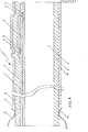
- the sensor shown in the partial section according to FIG. 1 comprises a flat substrate 10 made of a poorly conductive material such as quartz. A layer 2u of polycrystalline silicon is located on this substrate. These Layer 20 is provided with a cover 40 for the passivation.
- the substrate has a flat surface structure.
- the polycrystalline silicon layer 20 is applied by the chemical vapor deposition method, vapor deposition or sputtering, in a layer thickness of, for example, 0.5 ⁇ m.
- a van der Pauw figure for example, is produced with the aid of lithographic methods, as is shown in FIG. 2. At this point, however, it is particularly important to emphasize that this does not necessarily have to be a van der Pauw figure, but that other geometrically predetermined areas can also be formed.
- the layer 20 initially applied over the entire area is only retained in the area of these figures, while the silicon regions lying in between are etched away. Subsequently, the contact regions 60 of the resistance or van der Pauw figure are heavily predoped using a lithography and a doping process (sheet resistance 30 30 ⁇ ).
- the resistance figure 20 made of polycrystalline silicon is then subjected to one or more treatment steps, with a doping (typical sheet resistance 2 500 ⁇ ) first and a subsequent temperature treatment being carried out in a diffusion furnace.
- the typical treatment temperature is 9u0 to 1100 ° C.
- irradiation with a laser or an electron beam is carried out for recrystallization of the polycrystalline structure.
- Specified sheet resistances or other physical parameters are set, the properties of the polycrystalline silicon being changed by the laser radiation.
- the substrate 10 with the measuring figure 20 located thereon is coated over the entire area with a metal layer, which at can for example consist of aluminum and has a thickness of about 1 micron.
- a subsequent lithography and etching process defines conductor tracks 30, as shown in FIGS. 3 and 4.
- the conductor tracks 30 are connected to the measuring figures and, insofar as the figures are van der Pauw figures, are connected to the contact areas 60. 4 shows the connection of a conductor track 30 to the measuring figure 20 made of polycrystalline silicon.
- the ends 50 of the conductor tracks 30 lying on the outer edge of the sensor can carry a galvanic thickening, so that the sensor can be contacted by plugging into a standard plug.
- a contact strip can also be soldered to the conductor tracks 30.
- the contacting can also take place via a conventional gold wire bonding to the conductor tracks 3 0th
- the senor is passivated with a layer 4u (FIG. 1) for passivation.
- This can be a quartz or silicon nitride layer.
- a layer 40 of protective lacquer can also be applied by an immersion process or by spraying.
- the sensor 1 shown in FIGS. 5 and 6 comprises a low-resistance carrier substrate 3, which consists of silicon, with a specific resistance of, for example, ⁇ 1 ohm cm.
- This substrate 3 is, for example, thermally oxidized until a first SiO 2 layer 2 has grown as a substrate for the sensor measurement figure 6 with a layer thickness of approximately 1 ⁇ m. Then a standard lithography step is used an opening 4 for the rear-side contact 11 is etched into the first SiO 2 layer 2.
- the SiO 2 layer on the S cheiben Wegseite removed.
- the front of the substrate 3 is then covered with a layer of polycrystalline silicon, for example 0.5 ⁇ m thick.
- the next step is the definition of the sensor measurement figure 6 and a contact doping of the connection areas for the front side contact 12 and the rear side contact 11.
- the polysilicon layer is then processed in such a way that it is optimally suited for sensing the desired environmental parameter.
- the front of the substrate 2 is covered pyrolytically with an approximately 1 ⁇ m thick second SiO 2 layer 7, which also covers the sensor measuring figure 6.
- an opening 5 for the front-side contact 12 is produced within the second SiO 2 layer 7.
- the metallization of the sensor is carried out simply by vapor deposition on both sides of the second SiO 2 layer 7 on the front side of the sensor 1 on the one hand and of the carrier substrate 3 on the rear side thereof, with an approximately 1.5 ⁇ m thick aluminum layer 9 and an alloying step.
- the individual sensors are separated from one another by scoring and breaking or telling along the scoring or sawing paths 13.
- the contacting of the sensor 1 takes place via two clamping contacts 1u on the metallized front and rear sides 9 of the sensor 1, although other contacting, such as by soldering, is also possible without further ado.
- the sensor 1 can be provided with a passivation coating which is applied to the metallization 9 of the sensor 1 outside the engagement area of the clamping contacts 10.
- the passivation can consist of a quartz or silicon layer, or can also be formed by a protective lacquer which is applied by dip coating or spraying.
- the sensors can also consist of a combination of the sensors described above. This combination can be achieved both by arranging several of the individual sensors described next to one another and also by simultaneously placing a combination of the above-described sensors during production (integrated sensor).
- a special embodiment includes the manufacture and use of flow sensors according to the anemometer principle, with a heat source, e.g. B. a heated resistor. Depending on the direction of flow, the heat from this source is transferred to one or more of these sensors.
- a heat source e.g. B. a heated resistor.
Landscapes
- Physics & Mathematics (AREA)
- General Physics & Mathematics (AREA)
- Nonlinear Science (AREA)
- Pressure Sensors (AREA)
Priority Applications (1)
| Application Number | Priority Date | Filing Date | Title |
|---|---|---|---|
| AT82101524T ATE28933T1 (de) | 1981-03-16 | 1982-03-01 | Sensor zur messung physikalischer groessen sowie verfahren zu seiner herstellung und seine verwendung. |
Applications Claiming Priority (4)
| Application Number | Priority Date | Filing Date | Title |
|---|---|---|---|
| DE3110047 | 1981-03-16 | ||
| DE19813110047 DE3110047A1 (de) | 1981-03-16 | 1981-03-16 | Sensor zur messung physikalischer groessen sowie verfahren zu seiner herstellung und seine verwendung |
| DE3119750 | 1981-05-18 | ||
| DE19813119750 DE3119750A1 (de) | 1981-05-18 | 1981-05-18 | Sensor zur messung physikalischer groessen sowie verfahren zu seiner herstellung und seine verwendung |
Publications (3)
| Publication Number | Publication Date |
|---|---|
| EP0060427A2 true EP0060427A2 (fr) | 1982-09-22 |
| EP0060427A3 EP0060427A3 (en) | 1983-11-30 |
| EP0060427B1 EP0060427B1 (fr) | 1987-08-12 |
Family
ID=25791839
Family Applications (1)
| Application Number | Title | Priority Date | Filing Date |
|---|---|---|---|
| EP82101524A Expired EP0060427B1 (fr) | 1981-03-16 | 1982-03-01 | Elément sensible pour la mesure de dimensions physiques ainsi que procédé pour sa fabrication et son utilisation |
Country Status (2)
| Country | Link |
|---|---|
| EP (1) | EP0060427B1 (fr) |
| DE (1) | DE3276965D1 (fr) |
Cited By (4)
| Publication number | Priority date | Publication date | Assignee | Title |
|---|---|---|---|---|
| EP0075833A3 (fr) * | 1981-09-28 | 1983-11-30 | Siemens Aktiengesellschaft | Capteur de température à sémi-conducteur |
| FR2763127A1 (fr) * | 1997-05-12 | 1998-11-13 | France Etat | Thermometre a sonde jetable |
| WO2005057150A1 (fr) * | 2003-12-12 | 2005-06-23 | Georg Bernitz | Composant et son procede de fabrication |
| US7537963B2 (en) | 2003-11-28 | 2009-05-26 | Georg Bernitz | Device and method for manufacturing the same |
Family Cites Families (5)
| Publication number | Priority date | Publication date | Assignee | Title |
|---|---|---|---|---|
| US3406366A (en) * | 1966-01-13 | 1968-10-15 | Ibm | Electrical temperature sensor device |
| US3881181A (en) * | 1973-02-22 | 1975-04-29 | Rca Corp | Semiconductor temperature sensor |
| CA1040746A (fr) * | 1976-06-30 | 1978-10-17 | Robert W. Bertram | Thermistance en couche mince |
| DE2965814D1 (en) * | 1979-03-21 | 1983-08-11 | Bbc Brown Boveri & Cie | Thin film resistor having a high temperature coefficient and method of manufacturing the same |
| DE2944015C2 (de) * | 1979-10-31 | 1985-01-10 | Siemens AG, 1000 Berlin und 8000 München | Temperatursensor |
-
1982
- 1982-03-01 EP EP82101524A patent/EP0060427B1/fr not_active Expired
- 1982-03-01 DE DE8282101524T patent/DE3276965D1/de not_active Expired
Cited By (6)
| Publication number | Priority date | Publication date | Assignee | Title |
|---|---|---|---|---|
| EP0075833A3 (fr) * | 1981-09-28 | 1983-11-30 | Siemens Aktiengesellschaft | Capteur de température à sémi-conducteur |
| FR2763127A1 (fr) * | 1997-05-12 | 1998-11-13 | France Etat | Thermometre a sonde jetable |
| EP0878696A1 (fr) * | 1997-05-12 | 1998-11-18 | Etat-Francais représenté par le Délégué Général pour L'Armement | Thermomètre à sonde jetable |
| US7537963B2 (en) | 2003-11-28 | 2009-05-26 | Georg Bernitz | Device and method for manufacturing the same |
| WO2005057150A1 (fr) * | 2003-12-12 | 2005-06-23 | Georg Bernitz | Composant et son procede de fabrication |
| US7746213B2 (en) | 2003-12-12 | 2010-06-29 | Heinrich Zitzmann | Device and method for manufacturing the same |
Also Published As
| Publication number | Publication date |
|---|---|
| DE3276965D1 (en) | 1987-09-17 |
| EP0060427B1 (fr) | 1987-08-12 |
| EP0060427A3 (en) | 1983-11-30 |
Similar Documents
| Publication | Publication Date | Title |
|---|---|---|
| DE3916311C2 (de) | Mehrfach-Thermoelementfühler | |
| DE69005785T2 (de) | Elektrischer Widerstand in Chip-Bauweise für Oberflächenbestückung und Verfahren zu seiner Herstellung. | |
| DE69117374T2 (de) | SiC-Dünnschichtthermistor und Verfahren und Herstellungsverfahren. | |
| DE3630393C2 (de) | Widerstandsthermometer | |
| DE2742902A1 (de) | Absolutfeuchtigkeitsfuehler und verfahren zu deren herstellung | |
| DE1903961B2 (de) | Integrierte Halbleiterschaltung und Verfahren zu ihrer Herstellung | |
| DE68912830T2 (de) | Integrierter heizbarer Fühler. | |
| WO1998026260A1 (fr) | Resistance electrique avec au moins deux champs de contact sur un substrat en ceramique et son procede de fabrication | |
| EP1196747B1 (fr) | Dispositif de mesure de hautes temperatures et procede de fabrication dudit dispositif | |
| DE19512813C1 (de) | Verfahren zur Herstellung von Bauelementen | |
| DE10020932C5 (de) | Temperaturmessfühler und Verfahren zur Herstellung desselben | |
| EP0693677B1 (fr) | Dispositif d'alimentation en courant, en particulier pour des instruments de mesure à actionnement électrique | |
| EP0060427B1 (fr) | Elément sensible pour la mesure de dimensions physiques ainsi que procédé pour sa fabrication et son utilisation | |
| EP1248968B1 (fr) | Dispositif de mesure et de regulation de temperature | |
| DE3324272A1 (de) | Thermistor-bolometer | |
| DE3110047A1 (de) | Sensor zur messung physikalischer groessen sowie verfahren zu seiner herstellung und seine verwendung | |
| DE2644638C2 (fr) | ||
| EP0016263A1 (fr) | Résistance en couche mince à coefficient de température élevé et procédé pour sa fabrication | |
| EP0235359A2 (fr) | Dispositif pour mesurer la vitesse d'écoulement d'un fluide | |
| DE2513859C2 (de) | Verfahren zum Herstellen eines Kondensator-Widerstands-Netzwerks | |
| DE1791233B1 (de) | Verfahren zur Herstellung eines Funktionsblocks,insbesondere fuer datenverarbeitende Anlagen | |
| DE69938531T2 (de) | Verfahren zur herstellung eines sensors und eines widerstandselementes | |
| EP0235357A2 (fr) | Dispositif pour mesurer la vitesse d'écoulement d'un fluide | |
| DE3119750A1 (de) | Sensor zur messung physikalischer groessen sowie verfahren zu seiner herstellung und seine verwendung | |
| DE19832597A1 (de) | Substratstruktur mit Klebesäumen zur sicheren Verankerung und Verbindung eines vom Substrat getragenen Dünnfilms |
Legal Events
| Date | Code | Title | Description |
|---|---|---|---|
| PUAI | Public reference made under article 153(3) epc to a published international application that has entered the european phase |
Free format text: ORIGINAL CODE: 0009012 |
|
| AK | Designated contracting states |
Kind code of ref document: A2 Designated state(s): AT BE CH DE FR GB IT NL SE Designated state(s): AT BE CH DE FR GB IT NL SE |
|
| PUAL | Search report despatched |
Free format text: ORIGINAL CODE: 0009013 |
|
| AK | Designated contracting states |
Kind code of ref document: A3 Designated state(s): AT BE CH DE FR GB IT LI NL SE Designated state(s): AT BE CH DE FR GB IT LI NL SE |
|
| 17P | Request for examination filed |
Effective date: 19831224 |
|
| GRAA | (expected) grant |
Free format text: ORIGINAL CODE: 0009210 |
|
| AK | Designated contracting states |
Kind code of ref document: B1 Designated state(s): AT BE CH DE FR GB IT LI NL SE |
|
| PG25 | Lapsed in a contracting state [announced via postgrant information from national office to epo] |
Ref country code: NL Effective date: 19870812 Ref country code: IT Free format text: LAPSE BECAUSE OF FAILURE TO SUBMIT A TRANSLATION OF THE DESCRIPTION OR TO PAY THE FEE WITHIN THE PRESCRIBED TIME-LIMIT;WARNING: LAPSES OF ITALIAN PATENTS WITH EFFECTIVE DATE BEFORE 2007 MAY HAVE OCCURRED AT ANY TIME BEFORE 2007. THE CORRECT EFFECTIVE DATE MAY BE DIFFERENT FROM THE ONE RECORDED. Effective date: 19870812 Ref country code: FR Free format text: THE PATENT HAS BEEN ANNULLED BY A DECISION OF A NATIONAL AUTHORITY Effective date: 19870812 Ref country code: BE Effective date: 19870812 |
|
| REF | Corresponds to: |
Ref document number: 28933 Country of ref document: AT Date of ref document: 19870815 Kind code of ref document: T |
|
| PG25 | Lapsed in a contracting state [announced via postgrant information from national office to epo] |
Ref country code: SE Effective date: 19870831 |
|
| REF | Corresponds to: |
Ref document number: 3276965 Country of ref document: DE Date of ref document: 19870917 |
|
| NLV1 | Nl: lapsed or annulled due to failure to fulfill the requirements of art. 29p and 29m of the patents act | ||
| EN | Fr: translation not filed | ||
| PG25 | Lapsed in a contracting state [announced via postgrant information from national office to epo] |
Ref country code: AT Effective date: 19880301 |
|
| PLBE | No opposition filed within time limit |
Free format text: ORIGINAL CODE: 0009261 |
|
| STAA | Information on the status of an ep patent application or granted ep patent |
Free format text: STATUS: NO OPPOSITION FILED WITHIN TIME LIMIT |
|
| 26N | No opposition filed | ||
| PG25 | Lapsed in a contracting state [announced via postgrant information from national office to epo] |
Ref country code: GB Effective date: 19890301 |
|
| PGFP | Annual fee paid to national office [announced via postgrant information from national office to epo] |
Ref country code: DE Payment date: 19890318 Year of fee payment: 8 |
|
| PG25 | Lapsed in a contracting state [announced via postgrant information from national office to epo] |
Ref country code: LI Effective date: 19890331 Ref country code: CH Effective date: 19890331 |
|
| GBPC | Gb: european patent ceased through non-payment of renewal fee | ||
| REG | Reference to a national code |
Ref country code: CH Ref legal event code: PL |
|
| PG25 | Lapsed in a contracting state [announced via postgrant information from national office to epo] |
Ref country code: DE Effective date: 19901201 |