EP0060583B1 - Système pour la quantification de signaux - Google Patents
Système pour la quantification de signaux Download PDFInfo
- Publication number
- EP0060583B1 EP0060583B1 EP82200239A EP82200239A EP0060583B1 EP 0060583 B1 EP0060583 B1 EP 0060583B1 EP 82200239 A EP82200239 A EP 82200239A EP 82200239 A EP82200239 A EP 82200239A EP 0060583 B1 EP0060583 B1 EP 0060583B1
- Authority
- EP
- European Patent Office
- Prior art keywords
- signal
- quantizing
- output signal
- noise
- converter
- Prior art date
- Legal status (The legal status is an assumption and is not a legal conclusion. Google has not performed a legal analysis and makes no representation as to the accuracy of the status listed.)
- Expired
Links
- 238000013139 quantization Methods 0.000 title claims description 6
- 238000001228 spectrum Methods 0.000 claims description 13
- 238000012546 transfer Methods 0.000 claims description 10
- 238000005070 sampling Methods 0.000 description 12
- 238000010586 diagram Methods 0.000 description 9
- 230000005540 biological transmission Effects 0.000 description 6
- 238000010276 construction Methods 0.000 description 5
- 238000006243 chemical reaction Methods 0.000 description 4
- 230000001629 suppression Effects 0.000 description 4
- 238000007493 shaping process Methods 0.000 description 3
- 238000004891 communication Methods 0.000 description 2
- 230000008054 signal transmission Effects 0.000 description 2
- 238000013461 design Methods 0.000 description 1
- 238000011156 evaluation Methods 0.000 description 1
- 238000003672 processing method Methods 0.000 description 1
Images


Classifications
-
- H—ELECTRICITY
- H04—ELECTRIC COMMUNICATION TECHNIQUE
- H04B—TRANSMISSION
- H04B14/00—Transmission systems not characterised by the medium used for transmission
- H04B14/02—Transmission systems not characterised by the medium used for transmission characterised by the use of pulse modulation
- H04B14/04—Transmission systems not characterised by the medium used for transmission characterised by the use of pulse modulation using pulse code modulation
- H04B14/046—Systems or methods for reducing noise or bandwidth
-
- H—ELECTRICITY
- H03—ELECTRONIC CIRCUITRY
- H03M—CODING; DECODING; CODE CONVERSION IN GENERAL
- H03M3/00—Conversion of analogue values to or from differential modulation
- H03M3/30—Delta-sigma modulation
- H03M3/458—Analogue/digital converters using delta-sigma modulation as an intermediate step
- H03M3/46—Analogue/digital converters using delta-sigma modulation as an intermediate step using a combination of at least one delta-sigma modulator in series with at least one analogue/digital converter of a different type
-
- H—ELECTRICITY
- H03—ELECTRONIC CIRCUITRY
- H03M—CODING; DECODING; CODE CONVERSION IN GENERAL
- H03M3/00—Conversion of analogue values to or from differential modulation
- H03M3/30—Delta-sigma modulation
- H03M3/39—Structural details of delta-sigma modulators, e.g. incremental delta-sigma modulators
- H03M3/412—Structural details of delta-sigma modulators, e.g. incremental delta-sigma modulators characterised by the number of quantisers and their type and resolution
- H03M3/414—Structural details of delta-sigma modulators, e.g. incremental delta-sigma modulators characterised by the number of quantisers and their type and resolution having multiple quantisers arranged in cascaded loops, each of the second and further loops processing the quantisation error of the loop preceding it, i.e. multiple stage noise shaping [MASH] type
- H03M3/418—Structural details of delta-sigma modulators, e.g. incremental delta-sigma modulators characterised by the number of quantisers and their type and resolution having multiple quantisers arranged in cascaded loops, each of the second and further loops processing the quantisation error of the loop preceding it, i.e. multiple stage noise shaping [MASH] type all these quantisers being single bit quantisers
-
- H—ELECTRICITY
- H03—ELECTRONIC CIRCUITRY
- H03M—CODING; DECODING; CODE CONVERSION IN GENERAL
- H03M3/00—Conversion of analogue values to or from differential modulation
- H03M3/30—Delta-sigma modulation
- H03M3/39—Structural details of delta-sigma modulators, e.g. incremental delta-sigma modulators
- H03M3/412—Structural details of delta-sigma modulators, e.g. incremental delta-sigma modulators characterised by the number of quantisers and their type and resolution
- H03M3/422—Structural details of delta-sigma modulators, e.g. incremental delta-sigma modulators characterised by the number of quantisers and their type and resolution having one quantiser only
- H03M3/43—Structural details of delta-sigma modulators, e.g. incremental delta-sigma modulators characterised by the number of quantisers and their type and resolution having one quantiser only the quantiser being a single bit one
Definitions
- the invention relates to a system for the quantization of signals comprising, a transmitter section and a receiver section the transmitter section comprising quantizing means, a difference producer and filter means, an input signal and a quantized output signal which is derived from the quantizing means, and functions as a feedback signal being applied to the difference producer and a signal derived from the output signal of the difference producer being applied to the quantizing means, the latter serving to quantize the level of the signal derived from the output signal of the difference producer in a plurality of quantizing levels in order to produce a quantized output signal, filter means being connected in the path of the input signal for relatively influencing the spectrum of the quantizing noise with respect to the spectrum of the input signal.
- the invention may be employed in A/D and D/A-conversion and the conversion of a digital format into another digital format (D/D-conversion).
- the invention is employed in those signal processing methods in which, as an intermediate step, the number of quantizing levels of a signal is reduced and the sampling rate thereof is increased.
- the invention has for its object to provide a system for the quantization of signals as defined in section A(1) in which a second quantized signal is employed along with the principal quantized signal and in which, the performances as regards the reduction in quantizing noise remaining the same, the number of quantizing levels of the feedback signal can be reduced.
- the system is characterized in that the quantizing means are adapted for providing a second quantized output signal in response to the signal derived from the output signal of the difference producer and that in the receiver section a first received signal which is proportional to the first output signal of the transmitter section is applied to a first network having a first transfer function and a second received signal which is proportional to the second output signal of the transmitter section is applied to a second network having a second transfer function for relatively influencing the spectrum of the second received signal in a manner which is similar to the manner in which the said filter means influences the spectrum of the quantizing noise in the transmitter section and that the output signal of the first network is combined with the output signal of the second network for providing a receiver section output signal the transfer functions of the first and second networks being so determined relative to the transfer function of the transmitter section that on combining received signals the quantizing noise in the first received signal is cancelled by that portion of the quantizing noise in the second received signal which is proportional to the quantizing noise of the first quantized output signal of the quantizing means.
- the number of quantizing levels of the feedback signal may in principle amount to two in which case a one-bit D/A-converter may be employed in the feedback loop. A level unbalance may occur during said conversion.
- the DC-error voltage produced thereby is generally of little importance. Apart from this error voltage the one-bit converter behaves in a faultless manner, which is in contradistinction to multi-bit converters in which furthermore non-linearities may be produced owing to the threshold inaccuracies.
- X, Y, Z, U, V, . « : are the spectrum functions (Fourier transforms) of time signals; they are at the same time an indication of the relevant signal.
- G1, H1, 1/G1', H1', G2, Vietnamese: are transfer functions of networks (filters); they are at the same time an indication of the relevant network.
- Q1', Q2,7-8 are the spectrum functions of the quantizing noise: they are at the same time an indication of the relevant quantizer.
- the system 01 shown in figure 1 for quantizing signals comprises a transmitter section TR and a receiver section RC which are interconnected by means of a transmission path P.
- the transmitter section and the receiver section may be located very near to each other, for example in an integrated implementation on the same chip, or they may be some distance apart.
- the transmission path P may have any form suitable to transmit a signal Y and a signal U from the transmitter section TR to the receiver section RC.
- the received signals which are proportional to Y and U are denoted by Y' and U'.
- the transmitter section TR comprises quantizing means KW, a difference producer DF1 and filter means in the form of the networks G1 and H1.
- An input signal X and a quantized output signal Y which is derived from the quantizing means KW and functions as a feedback signal are applied to the difference producer DF1.
- the output signal of difference producer DF1 is applied by the network G1 to the quantizing means KW which serves to quantize the filtered output signal of the difference producer in a plurality of quantizing levels in order to produce a quantized output signal Y.
- the network G1 influences the spectrum of the input signal X relatively with respect to the spectrum of the quantizing noise in the output signal Y of the quantizing means KW.
- This network G1 has a noise-spectrum shaping action and, as will be apparent from reference D.2, there are several possibilities to introduce a noise-shaping network in a feedback quantizing arrangement.
- the networks H1 and G1 will have to be chosen such that their combination ensures the stability of the feedback loop.
- a relative suppression of the quantizing noise by the network G1 by adB. increases the dynamic range by adB.
- the quantizing means KW comprises a quantizer Q1' serving to provide the quantized output signal Y.
- the receiver section RC comprises a network H1' the input of which is connected in parallel through a summing device OP with the input a network 1/G1', the outputs of these networks being combined through a summing device SF1.
- a received signal Y' which is proportional to the quantized output signal Y of the transmitter section TR is applied to the input of the network H1' and, through the summing device OP, to the input of the network 1/G1', as a result of which an output signal Z of the receiver section is provided at the output of the summing device SF1 in accordance with the expression (2) if therein, for Q2, Q1' is read for the time being.
- expression (2) reduces to expression (3).
- the quantizing means KW comprises a quantizing arrangement Q2 for providing a second quantized output signal U in response to the filtered output signal of difference producer DF1 after the output signal Y of the quantizer Q1' has been in a difference producer AF subtracted.
- the input signal of the quantizing arrangement Q2 is then exactly the quantizing noise of quantizer Q1'.
- the quantizing arrangement Q2 has been chosen such that it quantizes the applied signal with an accuracy which is greater than the accuracy of the quantizer Q1'.
- the number of quantizing levels of the quantizing arrangement Q2 may be expressed in, for example, a number of eight bits, while quantizer Q1' is for example, a one-bit quantizer.
- a second received signal U' which is proportional to the second output signal U of the transmitter section TR is applied to the input of the network 1/G1' via summing device OP.
- the quantizing noise Q1' is not present in the output signal Z.
- the noise in the signal Y' which depends on the quantizing noise 01', is compensated for in summing device SF1 by the noise in the signal U' which also depends on the quantizing noise Q1'.
- an at least significant suppression of the quantizing noise Q1' in the output signal Z is realized.
- the quantizing noise contribution in the output signal Z becomes equal to Q2/G1.
- the quantizing arrangement Q2 has a greater accuracy during quantization than the quantizer 01' and a correspondingly lower quantizing noise (Q2 ⁇ Q1'). It will be noted that the compensation of the quantizing noise Q1' offers freedom in the choice of the number of quantizing levels of the quantizer Q1'. This number may even be reduced to two, which results in a very simple embodiment for quantizer Q1'.
- Figure 2 shows a second system Q1 in accordance with the invention, which differs from the system shown in Figure 1 in inter alia the absence of difference producer AF and summing device OP. A scrutiny of the two figures shows that the same output signal Z is obtained.
- the input signal V' of the network 1/G1' is the same in both cases.
- the quantizers Q1', Q2', etc in the systems Q1, 02, etc may each be in the form of a one-bit quantizer; at the same time quantizing arrangement QN in the (N-1 ) St system of the cascade may be in the form of a system having a feed- back one-bit quantizer QN'.
- the last system QN of the cascade will comprise in the receiver section RC the networks NH' and 1/GN' with parallel-arranged inputs. In this case the quantizing noise in the output signal Z may be expressed by
- FIG. 4 A variant of Figure 2 which is suitable for digital signal transmission is shown in Figure 4.
- a coder EC1' which codes the quantizing level, for example in a binary manner, is added to quantizer Q1'.
- the quantizer Q1' and the coder EC1' together form an analogue-to-digital converter A/D1'.
- quantizer Q2 forms an analogue-to-digital converter A/D2 in combination with coder EC2.
- a digital-to-analogue converter D/A1 is included in the path of the feed-back signal Y.
- the D/A-converters D/A1 and 1 D/A2 are connected in front of the networks H1' and 1/G1', respectively.
- the quantizer Q1' may be in the form of a one-bit quantizer. It is advantageous to opt for this construction, as in that case the D/A-converters D/A1 and D/A1' may be constructed as one-bit converters which do not produce noise which is commonly referred to as threshold inaccuracy noise, as would be the case with multi-bit D/A-converters (reference D.3).
- the noise contribution of D/A-converter 1D/A2 will be reduced by the network 1/G1' and plays a lesser part than the noise contributions of the converters D/A1 and D/A1'.
- nesting may also be used for the system Q1 of Figure 4 by giving the system comprising the A/D-converter A/D2 and the D/A-converter 1 D/A2 itself the same construction as the system Q1 shown in Figure 4. In this way the system of Figure 5 is derived from the system shown in Figure 4.
- a direct quantizing arrangement Q2 When a direct quantizing arrangement Q2 is used having more quantizing levels than the quantizer Q1 it is possible to derive the feedback signal Y in the system shown in Figure 4 from the output signal of A/D-converter A/D2, as is illustrated in Figure 6.
- a digital-to-digital converter D/D1 is arranged between the output of A/D-converter A/D2 and the input of D/A-converter D/A1. This D/D-converter converts each output code word of A/D-converter A/D2 into a code word having less bits.
- the quantizing levels of the quantizer Q1' simulated in this manner then form a sub-class of the quantizing levels of quantizing arrangement Q2, for example only the sign bit of the code word is maintained. This corresponds to the case in which the simulated quantizer Q1' is a one-bit quantizer.
- an identical D/D-converter D/D1' is arranged between the transmission path P and the input of D/A-converter D/A1'.
- This D/D-converter has here the same function as the D/D-converter D/D1 in the transmitter section TR, which results in a signal Y' which is proportional to the feedback signal Y being applied to the network H1'.
- A/D2, 1 D/A2 may be constructed as the system shown in Figure 6. Such a construction of the system in accordance with Figure 5 is illustrated in Figure 7.
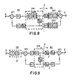
- the system in accordance with the invention may be employed in an analogue-to-digital converter arrangement.
- An embodiment of such a converter which is based on the system of Figure 6, is shown in Figure 8, the differences being inter alia that the converters D/A1', 1D/A2 and D/D1' have been omitted.
- the output signal of converter D/D1 is here directly applied to the input of the network H1'.
- the decimating digital low-pass filters DC1 and DC2 have for their object to reduce the sampling rate to a predetermined desired value, for example to the standard value of 8 kHz.
- the converter A/D2 may have, for example, a sampling rate of 128 kHz.
- the system in accordance with the invention may alternatively be used in a digital-to-analogue converter arrangement.
- An embodiment of such a converter which is based on the system shown in Figure 6 is shown in Figure 9.
- the differences compared with Figure 6 are inter alia the omission of the coder EC2 and the converters D/A1 and D/D1'.
- the output signal of converter D/D1 is here directly applied to the input of the converter D/A1'.
- the quantizer Q2 is a fully digital quantizer and may be in the form of a D/D-converter.
- An interpolating digital low-pass filter IF which serves to increase the sampling rate is connected between the input for the input signal X and the corresponding input of the (digital) difference producer DF1.
- the input signal has, for example, the standard sampling rate of 8 kHz for speech, while the system further operates with a sampling rate of 128 kHz.
- the system in accorduce with the invention may alternatively be used in a digital-to-digital converter arrangement.
- a converter arrangement of this type may simply be based on the converter arrangement shown in Figure 9 by omitting the converters D/A1' and 1 D/A2 therefrom.
Landscapes
- Engineering & Computer Science (AREA)
- Computer Networks & Wireless Communication (AREA)
- Signal Processing (AREA)
- Theoretical Computer Science (AREA)
- Compression, Expansion, Code Conversion, And Decoders (AREA)
- Analogue/Digital Conversion (AREA)
- Transmission Systems Not Characterized By The Medium Used For Transmission (AREA)
Claims (1)
- Système (Q1) pour la quantification de signaux comprenant une section d'émetteur (TR) et une section de récepteur (RC), la section d'émetteur (TR) comprenant des moyens de quantification (KW), un formateur de différence (DF1) et des moyens de filtrage (G1,H1), un signal d'entrée (X) et un signal de sortie quantifié (Y) qui est déduit des moyens de quantification (KW) et fonctionne comme un signal de réaction appliqué au formateur de différence (DF1) et un signal déduit du signal de sortie du formateur de différence (DF1 ) appliqué aux moyens de quantification (KW), ces derniers servant à quantifier le niveau du signal déduit du signal de sortie du formateur de différence (DF1) en plusieurs niveaux de quantification afin de produire un signal de sortie quantifié, des moyens de filtrage (G1) étant connectés dans le trajet du signal d'entrée (X) pour influencer relativement le spectre du bruit de quantification par rapport au spectre de signal d'entrée (X), caractérisé en ce que les moyens de quantification (KW) sont appropriés pour fournir un second signal de sortie quantifié (U) en réponse au signal déduit du signal de sortie du formateur de différence (DF1), en ce que dans la section de récepteur (RC), un premier signal reçu (Y') qui est proportionnel au premier signal de sortie (Y) de la section d'émetteur (TR) est appliqué à un premier réseau (H1) réalisant une première fonction de transfert et une second signal (U') reçu qui est proportionnel au second side sortie (U) de la section d'émetteur (TR) est appliqué à un second réseau (1/G1') réalisant une seconde fonction de transfert pour influencer relativement le spectre du second signal (U') reçu d'une manière semblable à celle selon laquelle les moyens de filtrage (G1) influencent le spectre du bruit de quantification dans la section d'émetteur (TR) et en ce que le signal de sortie du premier réseau (H1') est combiné (SF1) avec le signal de sortie du second réseau (1/G1') pour fournir un signal de sortie (Z) de la section de récepteur, les fonctions de transfert du premier et du second réseau (H1', 1/G1') étant ainsi déterminées par rapport à la fonction de transfert de la section d'émetteur (TR) d'une manière telle que, par la combinaison des signaux reçus, le bruit de quantification dans le premier signal (Y') reçu est annulé par la partie du bruit de quantification dans le second signal (U') reçu qui est proportionnelle au bruit de quantification du premier signal de sortie (Y) quantifié des moyens de quantification (KW).
Applications Claiming Priority (2)
| Application Number | Priority Date | Filing Date | Title |
|---|---|---|---|
| NL8101199A NL8101199A (nl) | 1981-03-12 | 1981-03-12 | Systeem voor het kwantiseren van signalen. |
| NL8101199 | 1981-03-12 |
Publications (2)
| Publication Number | Publication Date |
|---|---|
| EP0060583A1 EP0060583A1 (fr) | 1982-09-22 |
| EP0060583B1 true EP0060583B1 (fr) | 1985-01-30 |
Family
ID=19837148
Family Applications (1)
| Application Number | Title | Priority Date | Filing Date |
|---|---|---|---|
| EP82200239A Expired EP0060583B1 (fr) | 1981-03-12 | 1982-02-26 | Système pour la quantification de signaux |
Country Status (6)
| Country | Link |
|---|---|
| US (1) | US4468790A (fr) |
| EP (1) | EP0060583B1 (fr) |
| JP (1) | JPS57160235A (fr) |
| CA (1) | CA1178679A (fr) |
| DE (1) | DE3262083D1 (fr) |
| NL (1) | NL8101199A (fr) |
Families Citing this family (37)
| Publication number | Priority date | Publication date | Assignee | Title |
|---|---|---|---|---|
| DE3232558A1 (de) * | 1982-09-01 | 1984-03-01 | Siemens AG, 1000 Berlin und 8000 München | Digitaler dpcm-kodierer mit hoher verarbeitungsgeschwindigkeit |
| US4616349A (en) * | 1982-11-22 | 1986-10-07 | Mobil Oil Corporation | Analog-to-digital converter for seismic exploration using delta modulation |
| DE3679680D1 (de) * | 1985-02-04 | 1991-07-18 | Nippon Telegraph & Telephone | Konverter mit ueberabtastung. |
| US4727506A (en) * | 1985-03-25 | 1988-02-23 | Rca Corporation | Digital scaling circuitry with truncation offset compensation |
| US4853969A (en) * | 1987-01-13 | 1989-08-01 | Recognition Equipment Incorporated | Quantized digital filter |
| US4866442A (en) * | 1987-06-01 | 1989-09-12 | Steim Joseph M | Analog to digital converter employing delta-sigma modulation |
| FR2625060B1 (fr) * | 1987-12-16 | 1990-10-05 | Guichard Jacques | Procede et dispositifs de codage et de decodage pour la transmission d'images a travers un reseau a debit variable |
| US4876542A (en) * | 1988-01-25 | 1989-10-24 | Motorola, Inc. | Multiple output oversampling A/D converter with each output containing data and noise |
| US4862169A (en) * | 1988-03-25 | 1989-08-29 | Motorola, Inc. | Oversampled A/D converter using filtered, cascaded noise shaping modulators |
| US5210623A (en) * | 1989-12-21 | 1993-05-11 | Eastman Kodak Company | Apparatus and method for quantizing and/or reconstructing multi-dimensional digital image signals |
| US5103229A (en) * | 1990-04-23 | 1992-04-07 | General Electric Company | Plural-order sigma-delta analog-to-digital converters using both single-bit and multiple-bit quantization |
| NL9001440A (nl) * | 1990-06-22 | 1992-01-16 | Philips Nv | Analoog/digitaal signaal-omvormer met meervoudige sigma-delta modulator. |
| FR2671680B1 (fr) * | 1991-01-16 | 1993-04-30 | Texas Instruments France | Modulateur delta-sigma notamment pour convertisseur analogique-numerique a plage dynamique et a linearite elevees. |
| TW272341B (fr) * | 1993-07-16 | 1996-03-11 | Sony Co Ltd | |
| US5442354A (en) * | 1993-08-26 | 1995-08-15 | Advanced Micro Devices, Inc. | Fourth-order cascaded sigma-delta modulator |
| US5774844A (en) * | 1993-11-09 | 1998-06-30 | Sony Corporation | Methods and apparatus for quantizing, encoding and decoding and recording media therefor |
| WO1996031943A2 (fr) * | 1995-04-03 | 1996-10-10 | Philips Electronics N.V. | Convertisseur de signaux en quadrature |
| US7035607B2 (en) * | 1998-05-29 | 2006-04-25 | Silicon Laboratories Inc. | Systems and methods for providing an adjustable reference signal to RF circuitry |
| US6970717B2 (en) | 2001-01-12 | 2005-11-29 | Silicon Laboratories Inc. | Digital architecture for radio-frequency apparatus and associated methods |
| US6804497B2 (en) | 2001-01-12 | 2004-10-12 | Silicon Laboratories, Inc. | Partitioned radio-frequency apparatus and associated methods |
| US7092675B2 (en) * | 1998-05-29 | 2006-08-15 | Silicon Laboratories | Apparatus and methods for generating radio frequencies in communication circuitry using multiple control signals |
| US7242912B2 (en) * | 1998-05-29 | 2007-07-10 | Silicon Laboratories Inc. | Partitioning of radio-frequency apparatus |
| US7024221B2 (en) * | 2001-01-12 | 2006-04-04 | Silicon Laboratories Inc. | Notch filter for DC offset reduction in radio-frequency apparatus and associated methods |
| US7228109B2 (en) * | 2001-01-12 | 2007-06-05 | Silicon Laboratories Inc. | DC offset reduction in radio-frequency apparatus and associated methods |
| US6993314B2 (en) | 1998-05-29 | 2006-01-31 | Silicon Laboratories Inc. | Apparatus for generating multiple radio frequencies in communication circuitry and associated methods |
| US7221921B2 (en) * | 1998-05-29 | 2007-05-22 | Silicon Laboratories | Partitioning of radio-frequency apparatus |
| US6903617B2 (en) | 2000-05-25 | 2005-06-07 | Silicon Laboratories Inc. | Method and apparatus for synthesizing high-frequency signals for wireless communications |
| US7138858B2 (en) | 2001-01-12 | 2006-11-21 | Silicon Laboratories, Inc. | Apparatus and methods for output buffer circuitry with constant output power in radio-frequency circuitry |
| US7035611B2 (en) * | 2001-01-12 | 2006-04-25 | Silicon Laboratories Inc. | Apparatus and method for front-end circuitry in radio-frequency apparatus |
| US20030232613A1 (en) * | 2001-01-12 | 2003-12-18 | Kerth Donald A. | Quadrature signal generation in radio-frequency apparatus and associated methods |
| US7177610B2 (en) * | 2001-01-12 | 2007-02-13 | Silicon Laboratories Inc. | Calibrated low-noise current and voltage references and associated methods |
| US7031683B2 (en) * | 2001-01-12 | 2006-04-18 | Silicon Laboratories Inc. | Apparatus and methods for calibrating signal-processing circuitry |
| US7158574B2 (en) * | 2001-01-12 | 2007-01-02 | Silicon Laboratories Inc. | Digital interface in radio-frequency apparatus and associated methods |
| US8467483B2 (en) * | 2002-03-15 | 2013-06-18 | Silicon Laboratories Inc. | Radio-frequency apparatus and associated methods |
| DE10233392B4 (de) * | 2002-07-23 | 2006-08-17 | Infineon Technologies Ag | Analog/Digital-Modulator |
| KR100558481B1 (ko) * | 2003-01-03 | 2006-03-07 | 삼성전자주식회사 | 양자화 잡음을 감소시킬 수 있는 델타 시그마 변조기 |
| JP2004260708A (ja) * | 2003-02-27 | 2004-09-16 | Mitsumi Electric Co Ltd | 通信システム及び通信装置 |
Family Cites Families (3)
| Publication number | Priority date | Publication date | Assignee | Title |
|---|---|---|---|---|
| US2516587A (en) * | 1947-12-03 | 1950-07-25 | Bell Telephone Labor Inc | Correction of errors in pulse code communication |
| JPS5114846B1 (fr) * | 1968-08-08 | 1976-05-12 | ||
| NL174611C (nl) * | 1975-06-12 | 1984-07-02 | Philips Nv | Differentieel pulscodemodulatie overdrachtstelsel. |
-
1981
- 1981-03-12 NL NL8101199A patent/NL8101199A/nl not_active Application Discontinuation
-
1982
- 1982-02-16 US US06/349,233 patent/US4468790A/en not_active Expired - Fee Related
- 1982-02-26 DE DE8282200239T patent/DE3262083D1/de not_active Expired
- 1982-02-26 EP EP82200239A patent/EP0060583B1/fr not_active Expired
- 1982-03-11 CA CA000398108A patent/CA1178679A/fr not_active Expired
- 1982-03-12 JP JP57038229A patent/JPS57160235A/ja active Pending
Non-Patent Citations (1)
| Title |
|---|
| IEEE TRANSACTIONS ON CIRCUITS AND SYSTEMS, vol. CAS-25, no. 7, July 1978, pages 436-447, New York (USA); S.K. TEWKSBURY et al.: "Oversampled, linear predictive and noise-shaping coders of order N > 1" * |
Also Published As
| Publication number | Publication date |
|---|---|
| NL8101199A (nl) | 1982-10-01 |
| DE3262083D1 (en) | 1985-03-14 |
| JPS57160235A (en) | 1982-10-02 |
| CA1178679A (fr) | 1984-11-27 |
| EP0060583A1 (fr) | 1982-09-22 |
| US4468790A (en) | 1984-08-28 |
Similar Documents
| Publication | Publication Date | Title |
|---|---|---|
| US4468790A (en) | System for the quantization of signals | |
| CA1112366A (fr) | Dispositif de conversion du mode analogue au mode numerique | |
| US4467316A (en) | Generalized interpolative method for digital/analog conversion of PCM signals | |
| US4593267A (en) | Digital data code conversion circuit for variable-word-length data code | |
| EP0288281B1 (fr) | Systèmes de codage et de décodage MICDA | |
| US4592070A (en) | ADPCM encoder/decoder with improved tracking | |
| US3949299A (en) | Signal coding for telephone communication system | |
| US4301446A (en) | Digital transmission system with a double analog integrator Delta Sigma coder and a double digital integrator Delta Sigma decoder | |
| HU187522B (en) | Delta-sygma modulator with switched condensers | |
| US4386237A (en) | NIC Processor using variable precision block quantization | |
| EP0463686B1 (fr) | Convertisseur de signal analogique/numérique muni d'un modulateur multiple sigma-delta | |
| US4016410A (en) | Signal processor with digital filter and integrating network | |
| EP0283167A2 (fr) | Codeur et décodeur numérique/analogique pour signal audio | |
| US4191858A (en) | Block digital processing system for nonuniformly encoded digital words | |
| CA1219373A (fr) | Circuit de decodage adaptatif pour modulation differentielle par impulsions et codage | |
| JPH0234498B2 (fr) | ||
| NL7811731A (nl) | (b+a)-bits-a/d-omzetter met b-bits-hulp-a/d-omzetter. | |
| EP0131005A1 (fr) | Décodeur de code numérique. | |
| US3772682A (en) | Digital conversion from one pcm format to another | |
| US4542516A (en) | ADPCM Encoder/decoder with zero code suppression | |
| US5008672A (en) | Signal conversion apparatus which reduces quantization errors for telecommunications applications | |
| US6738002B2 (en) | SD-ADC with digital dither signal processing | |
| Boddie et al. | Digital signal processor: Adaptive differential pulse-code-modulation coding | |
| US4498173A (en) | Technique for digital split-channel transmission using interpolative coders and decoders | |
| US6570512B1 (en) | Circuit configuration for quantization of digital signals and for filtering quantization noise |
Legal Events
| Date | Code | Title | Description |
|---|---|---|---|
| PUAI | Public reference made under article 153(3) epc to a published international application that has entered the european phase |
Free format text: ORIGINAL CODE: 0009012 |
|
| 17P | Request for examination filed |
Effective date: 19820226 |
|
| AK | Designated contracting states |
Kind code of ref document: A1 Designated state(s): BE DE FR GB IT SE Designated state(s): BE DE FR GB IT SE |
|
| RAP1 | Party data changed (applicant data changed or rights of an application transferred) |
Owner name: N.V. PHILIPS' GLOEILAMPENFABRIEKEN |
|
| ITF | It: translation for a ep patent filed | ||
| GRAA | (expected) grant |
Free format text: ORIGINAL CODE: 0009210 |
|
| AK | Designated contracting states |
Kind code of ref document: B1 Designated state(s): BE DE FR GB IT SE Designated state(s): BE DE FR GB IT SE |
|
| REF | Corresponds to: |
Ref document number: 3262083 Country of ref document: DE Date of ref document: 19850314 |
|
| ET | Fr: translation filed | ||
| PLBE | No opposition filed within time limit |
Free format text: ORIGINAL CODE: 0009261 |
|
| STAA | Information on the status of an ep patent application or granted ep patent |
Free format text: STATUS: NO OPPOSITION FILED WITHIN TIME LIMIT |
|
| 26N | No opposition filed | ||
| PGFP | Annual fee paid to national office [announced via postgrant information from national office to epo] |
Ref country code: BE Payment date: 19890203 Year of fee payment: 8 |
|
| PGFP | Annual fee paid to national office [announced via postgrant information from national office to epo] |
Ref country code: FR Payment date: 19890221 Year of fee payment: 8 |
|
| PGFP | Annual fee paid to national office [announced via postgrant information from national office to epo] |
Ref country code: SE Payment date: 19890224 Year of fee payment: 8 |
|
| ITTA | It: last paid annual fee | ||
| PGFP | Annual fee paid to national office [announced via postgrant information from national office to epo] |
Ref country code: GB Payment date: 19890228 Year of fee payment: 8 |
|
| PGFP | Annual fee paid to national office [announced via postgrant information from national office to epo] |
Ref country code: DE Payment date: 19890424 Year of fee payment: 8 |
|
| PG25 | Lapsed in a contracting state [announced via postgrant information from national office to epo] |
Ref country code: GB Effective date: 19900226 |
|
| PG25 | Lapsed in a contracting state [announced via postgrant information from national office to epo] |
Ref country code: SE Effective date: 19900227 |
|
| PG25 | Lapsed in a contracting state [announced via postgrant information from national office to epo] |
Ref country code: BE Effective date: 19900228 |
|
| BERE | Be: lapsed |
Owner name: N.V. PHILIPS' GLOEILAMPENFABRIEKEN Effective date: 19900228 |
|
| GBPC | Gb: european patent ceased through non-payment of renewal fee | ||
| PG25 | Lapsed in a contracting state [announced via postgrant information from national office to epo] |
Ref country code: FR Effective date: 19901031 |
|
| PG25 | Lapsed in a contracting state [announced via postgrant information from national office to epo] |
Ref country code: DE Effective date: 19901101 |
|
| REG | Reference to a national code |
Ref country code: FR Ref legal event code: ST |
|
| EUG | Se: european patent has lapsed |
Ref document number: 82200239.0 Effective date: 19901107 |