EP0060623B1 - Antenne à microbandes - Google Patents
Antenne à microbandes Download PDFInfo
- Publication number
- EP0060623B1 EP0060623B1 EP82300752A EP82300752A EP0060623B1 EP 0060623 B1 EP0060623 B1 EP 0060623B1 EP 82300752 A EP82300752 A EP 82300752A EP 82300752 A EP82300752 A EP 82300752A EP 0060623 B1 EP0060623 B1 EP 0060623B1
- Authority
- EP
- European Patent Office
- Prior art keywords
- array
- strip
- cell
- axis
- transverse
- Prior art date
- Legal status (The legal status is an assumption and is not a legal conclusion. Google has not performed a legal analysis and makes no representation as to the accuracy of the status listed.)
- Expired
Links
- 230000005855 radiation Effects 0.000 claims description 11
- 239000000758 substrate Substances 0.000 claims description 4
- 239000004020 conductor Substances 0.000 claims description 2
- 230000000694 effects Effects 0.000 claims description 2
- 238000003491 array Methods 0.000 description 8
- 238000009795 derivation Methods 0.000 description 2
- 230000007717 exclusion Effects 0.000 description 2
- 230000014509 gene expression Effects 0.000 description 2
- 238000005259 measurement Methods 0.000 description 1
- 239000002184 metal Substances 0.000 description 1
- 239000000843 powder Substances 0.000 description 1
- 230000000717 retained effect Effects 0.000 description 1
Images



Classifications
-
- H—ELECTRICITY
- H01—ELECTRIC ELEMENTS
- H01Q—ANTENNAS, i.e. RADIO AERIALS
- H01Q11/00—Electrically-long antennas having dimensions more than twice the shortest operating wavelength and consisting of conductive active radiating elements
- H01Q11/02—Non-resonant antennas, e.g. travelling-wave antenna
- H01Q11/04—Non-resonant antennas, e.g. travelling-wave antenna with parts bent, folded, shaped, screened or electrically loaded to obtain desired phase relation of radiation from selected sections of the antenna
-
- H—ELECTRICITY
- H01—ELECTRIC ELEMENTS
- H01Q—ANTENNAS, i.e. RADIO AERIALS
- H01Q13/00—Waveguide horns or mouths; Slot antennas; Leaky-waveguide antennas; Equivalent structures causing radiation along the transmission path of a guided wave
- H01Q13/20—Non-resonant leaky-waveguide or transmission-line antennas; Equivalent structures causing radiation along the transmission path of a guided wave
- H01Q13/206—Microstrip transmission line antennas
-
- H—ELECTRICITY
- H01—ELECTRIC ELEMENTS
- H01Q—ANTENNAS, i.e. RADIO AERIALS
- H01Q21/00—Antenna arrays or systems
- H01Q21/06—Arrays of individually energised antenna units similarly polarised and spaced apart
- H01Q21/061—Two dimensional planar arrays
- H01Q21/068—Two dimensional planar arrays using parallel coplanar travelling wave or leaky wave aerial units
-
- H—ELECTRICITY
- H01—ELECTRIC ELEMENTS
- H01Q—ANTENNAS, i.e. RADIO AERIALS
- H01Q21/00—Antenna arrays or systems
- H01Q21/24—Combinations of antenna units polarised in different directions for transmitting or receiving circularly and elliptically polarised waves or waves linearly polarised in any direction
Definitions
- This invention relates to stripline antennas, in particular to stripline antenna arrays.
- the polarisation direction depends on the lengths of the transverse and longitudinal sections of the strip in each quartet in relation to the operating wavelength in the strip, and the Application describes arrays in which these lengths produce vertical, horizontal or circular polarisation respectively, all in a direction normal to the plane of the array, ie the so-caiied broadside radiation.
- EP-A-7222 there is described, with reference to Figure 5 thereof, a system for varying the distribution of power radiated across the aperture constituted by such an array, in which the strip-width is made to increase progressively towards the centre of the aperture so that more power is radiated from the centre.
- the present invention provides a stripline antenna array in which the power distribution is varied by an alternative arrangement.
- the present invention may provide an array as aforesaid wherein the lengths of the transverse sections, as between cells, satisfy equations (15) or (16) hereinafter in relation to the required power distribution.
- a dielectric sheet 10 originally metal-coated on both faces, has one face etched to form a strip-line 11, leaving the other face to act as a ground-plane (not shown).
- the strip 11 turns through six successive right-angle corners 1-6 to form a cell constituted by three equispaced transverse sections extending from the axis x, the first section being of length s, the second section extending back across axis x and being of length s+p, and the third section being of length p, whose outward extremities are connected by two sections of length d.
- This cell whose extent is indicated by arrow 12, is joined to a succeeding similar cell having corners 1' ⁇ 6' by a length of strip L, and the complete array, comprising a relatively large number of such cells, is terminated by a matched load 13.
- the radiation from such right-angle corners is predominantly diagonal, and its equivalent circuit can be represented by the radiation conductance in parallel with a capacitative component.
- the corners may be truncated as described therein.
- Each cell shown in Figure 1 can be considered as having a diagonally polarised magnetic dipole source at each right-angle corner, the dipoles being fed in phase progression to form a travelling-wave array.
- the field in the plane of the array length only will be considered, ie the x-z or 8 plane in Figure 1, where z is normal to the plane of the array.
- the path-difference from sources 1 and 2 to a far-field point is zero. It can then be shown that the far-field components radiated in the 8 (ie x-z) plane are
- E is the magnetic dipole strength
- E T (8) is the transverse component of E (ie parallel to the x-y plane in Figure 1)
- u ⁇ k o dcos ⁇
- the strip-length L between successive cells is required.
- m is an integer giving the smallest L ⁇ 0.
- Figure 1 thus reduces to Figure 2 (extent of single cell shown dashed), which corresponds to Figure 4 of the European Application.
- Figure 1 thus reduces to Figure 3, which corresponds to Figure 2 of the European Application.
- Figure 3 corresponds to Figure 2 of the European Application.
- the extent of each single cell in the present Figure 3 (shown dashed) is defined differently from in the aforesaid Figure 2 for clarity, but the resulting array structures are identical.
- Figure 1 thus reduces to Figure 4, which corresponds to Figure 3 of the European Application. (The above comment about defining the extent of each cell applies here also, and less markedly to present Figure 2.)
- equation (12) allows E to be selected by appropriate choice of s.
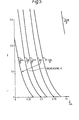
- the major axis of the polarisation ellipse lies along the direction of either E A or E T , depending the value of E. Curves of E against s for various values of d are plotted in Figure 5.
- Equation (13) can be solved numerically, and some values of d/ ⁇ m for given values of s/ ⁇ m and ⁇ are given in the following Table:
- Each Figure shows three successive cells, although in practice an array will have many more than three cells, eg ten.
- each cell has six actual corners; in Figures 7(k)-(o) these reduce to four actual corners because the inter-cell strip-length reduces to zero.
- the distribution of power radiated across the aperture constituted by the array can be varied in the manner described in the aforementioned European Application with reference to Figure 5 thereof, ie by making the strip-width increase progressively towards the centre so that more powder is radiated from the centre.
- this effect can be obtained in the manner described in a European Patent Application of even date and identical title by the present applicant in which the cell dimensions are varied progressively towards the centre.
- One array embodying the invention is shown in silhouette in Figure 8, in which the power distribution across the aperture is controlled by increasing the strip-width towards the centre.
- the aim was an HP array giving the coverage in the 8 plane indicated in Figure 9, having low side-lobes in the region 120° ⁇ 8 ⁇ 180°.
- the strip-width and correction to account for the corner susceptance are determined empirically.
- the position of the coaxial output connector 14 and the match thereto are important in this embodiment, as unwanted radiation from the connector, and the reflected wave created by any mismatch, are found to limit the achievable side-lobe level.
- Figure 8 shows the optimum connector position.
- Figure 10 shows the actual coverage in the 8 plane obtained with the ten-cell version (Figure 8), which may be compared with the desired coverage shown in Figure 9.
- the total power, P T , radiated by each cell of the array, assuming that the main beam is in the 8 plane, is given by where c is an arbitrary constant, the 8 plane is normal to, and includes, the axis of the array, and ET and E A are respectively the transverse and axial components of magnetic dipole strength (directions defined in the companion Application) for a given cell.
- E is the magnetic dipole strength
- s is the length of the transverse strip section either side of the array axis
- ⁇ is the wave-number in the stripline, as more fully explained in the companion Application.
- equations (15) or (16) Knowing the required power distribution across the effective radiating aperture, ie the respective powers from successive cells along the array, the particular value of P T required from each cell is inserted separately in equations (15) or (16) above to determine s/ ⁇ m for each cell.
- cE 2 in equations (15) or (16) can be determined by measurement, eg by measuring the power radiated by an array of identical cells and dividing by the number of cells in that array.
- equations (4), (8) and (10) in the companion Application allow d/ ⁇ m to be determined for each cell, and equation (11) therein gives L, where d is the length of the longitudinal strip sections in each cell and L is the strip-length between successive cells.
Landscapes
- Variable-Direction Aerials And Aerial Arrays (AREA)
Claims (3)


Applications Claiming Priority (2)
| Application Number | Priority Date | Filing Date | Title |
|---|---|---|---|
| GB8106781 | 1981-03-04 | ||
| GB8106781 | 1981-03-04 |
Publications (2)
| Publication Number | Publication Date |
|---|---|
| EP0060623A1 EP0060623A1 (fr) | 1982-09-22 |
| EP0060623B1 true EP0060623B1 (fr) | 1986-07-30 |
Family
ID=10520133
Family Applications (1)
| Application Number | Title | Priority Date | Filing Date |
|---|---|---|---|
| EP82300752A Expired EP0060623B1 (fr) | 1981-03-04 | 1982-02-15 | Antenne à microbandes |
Country Status (4)
| Country | Link |
|---|---|
| US (1) | US4459594A (fr) |
| EP (1) | EP0060623B1 (fr) |
| CA (1) | CA1183601A (fr) |
| DE (1) | DE3272236D1 (fr) |
Families Citing this family (5)
| Publication number | Priority date | Publication date | Assignee | Title |
|---|---|---|---|---|
| US5123039A (en) * | 1988-01-06 | 1992-06-16 | Jupiter Toy Company | Energy conversion using high charge density |
| US5018180A (en) * | 1988-05-03 | 1991-05-21 | Jupiter Toy Company | Energy conversion using high charge density |
| FI118193B (fi) * | 2005-07-04 | 2007-08-15 | Pentti Lajunen | Mittausjärjestelmä, mittausmenetelmä ja antennin uusi käyttö |
| TWI738343B (zh) * | 2020-05-18 | 2021-09-01 | 為昇科科技股份有限公司 | 蜿蜒天線結構 |
| CN112366445B (zh) * | 2020-10-27 | 2021-07-27 | 东莞市振亮精密科技有限公司 | 一种功分网络、5g天线模块及5g天线模块的装配方法 |
Family Cites Families (8)
| Publication number | Priority date | Publication date | Assignee | Title |
|---|---|---|---|---|
| FR1123769A (fr) * | 1955-03-17 | 1956-09-27 | Csf | Aérien incorporable pour engins mobiles |
| US3231894A (en) * | 1960-06-23 | 1966-01-25 | Sony Corp | Zigzag antenna |
| GB1269633A (en) * | 1968-05-09 | 1972-04-06 | Emi Ltd | Improvements relating to microwave antenna arrays |
| US3689929A (en) * | 1970-11-23 | 1972-09-05 | Howard B Moody | Antenna structure |
| FI379774A7 (fr) * | 1974-12-31 | 1976-07-01 | Martti Eelis Tiuri | |
| US4180817A (en) * | 1976-05-04 | 1979-12-25 | Ball Corporation | Serially connected microstrip antenna array |
| JPS5923123B2 (ja) * | 1976-08-30 | 1984-05-31 | 新日本無線株式会社 | マイクロ・ストリツプライン・アンテナ装置 |
| US4335385A (en) * | 1978-07-11 | 1982-06-15 | The Secretary Of State For Defence In Her Britannic Majesty's Government Of The United Kingdom Of Great Britain And Northern Ireland | Stripline antennas |
-
1982
- 1982-02-15 DE DE8282300752T patent/DE3272236D1/de not_active Expired
- 1982-02-15 EP EP82300752A patent/EP0060623B1/fr not_active Expired
- 1982-02-23 US US06/351,099 patent/US4459594A/en not_active Expired - Lifetime
- 1982-03-03 CA CA000397489A patent/CA1183601A/fr not_active Expired
Also Published As
| Publication number | Publication date |
|---|---|
| DE3272236D1 (en) | 1986-09-04 |
| US4459594A (en) | 1984-07-10 |
| CA1183601A (fr) | 1985-03-05 |
| EP0060623A1 (fr) | 1982-09-22 |
Similar Documents
| Publication | Publication Date | Title |
|---|---|---|
| Chopra et al. | Series-fed binomial microstrip arrays for extremely low sidelobe level | |
| Hayashi et al. | Millimeter-wave microstrip comb-line antenna using reflection-canceling slit structure | |
| Huang et al. | A low profile and low sidelobe wideband slot antenna array feb by an amplitude-tapering waveguide feed-network | |
| US9705199B2 (en) | Quasi TEM dielectric travelling wave scanning array | |
| Sun et al. | A wideband base station antenna element with stable radiation pattern and reduced beam squint | |
| US3987454A (en) | Log-periodic longitudinal slot antenna array excited by a waveguide with a conductive ridge | |
| EP0007222A1 (fr) | Antennes microbande | |
| Mailloux | An overlapped subarray for limited scan application | |
| Yang et al. | A single-layer circularly polarized antenna with improved gain based on quarter-mode substrate integrated waveguide cavities array | |
| AU614651B2 (en) | Slot array antenna | |
| Liu et al. | A 2-D circularly polarized fixed-frequency beam-scanning leakywave antenna for millimeter-wave satellite communications | |
| EP0061831A1 (fr) | Antenne à microbandes | |
| Kim et al. | Slot-coupled circularly polarized array antenna with substrate-integrated waveguide cavity for parallel-plate-mode suppression | |
| Chen et al. | A cross-polarization suppressed probe-fed patch antenna and its applications to wide-angle beam-scanning arrays | |
| EP0060623B1 (fr) | Antenne à microbandes | |
| JP2564410B2 (ja) | 二重モードログ周期ダイポールアンテナ | |
| Zhao et al. | A low-profile magnetoelectric dipole antenna based on comb structure and its application in frequency-scanning array with ground | |
| Stegen et al. | Arrays of closely-spaced nonresonant slots | |
| Moghaddam et al. | Compact beamforming network for producing multiple orthogonal beams in a limited field of view phased array antenna | |
| Deng et al. | Single-ridged waveguide antenna for X-band applications | |
| Zhang et al. | Enhanced-Bandwidth Center-Fed Linear Slot Array and Its Multibeam Application | |
| US12278436B2 (en) | Antenna device and array antenna device | |
| van de Ven et al. | E-Band Automotive Radar Array Antenna in Multi-Layer Waveguide Technology With Reduced Sidelobe and Cross-Polarization Level | |
| Miura et al. | Bandwidth enhancement of a series-fed microstrip patch array antenna | |
| Neophytou et al. | A Circularly-Polarized Zero Beam-Squinting Leaky-Wave Antenna Using NRI-TL Metamaterials with Increased Gain |
Legal Events
| Date | Code | Title | Description |
|---|---|---|---|
| PUAI | Public reference made under article 153(3) epc to a published international application that has entered the european phase |
Free format text: ORIGINAL CODE: 0009012 |
|
| AK | Designated contracting states |
Kind code of ref document: A1 Designated state(s): DE FR GB IT NL Designated state(s): DE FR GB IT NL |
|
| 17P | Request for examination filed |
Effective date: 19830304 |
|
| ITF | It: translation for a ep patent filed | ||
| GRAA | (expected) grant |
Free format text: ORIGINAL CODE: 0009210 |
|
| AK | Designated contracting states |
Kind code of ref document: B1 Designated state(s): DE FR GB IT NL |
|
| REF | Corresponds to: |
Ref document number: 3272236 Country of ref document: DE Date of ref document: 19860904 |
|
| ET | Fr: translation filed | ||
| PLBE | No opposition filed within time limit |
Free format text: ORIGINAL CODE: 0009261 |
|
| STAA | Information on the status of an ep patent application or granted ep patent |
Free format text: STATUS: NO OPPOSITION FILED WITHIN TIME LIMIT |
|
| 26N | No opposition filed | ||
| ITTA | It: last paid annual fee | ||
| PGFP | Annual fee paid to national office [announced via postgrant information from national office to epo] |
Ref country code: FR Payment date: 20010111 Year of fee payment: 20 |
|
| PGFP | Annual fee paid to national office [announced via postgrant information from national office to epo] |
Ref country code: GB Payment date: 20010118 Year of fee payment: 20 |
|
| PGFP | Annual fee paid to national office [announced via postgrant information from national office to epo] |
Ref country code: DE Payment date: 20010119 Year of fee payment: 20 |
|
| PGFP | Annual fee paid to national office [announced via postgrant information from national office to epo] |
Ref country code: NL Payment date: 20010129 Year of fee payment: 20 |
|
| REG | Reference to a national code |
Ref country code: GB Ref legal event code: IF02 |
|
| PG25 | Lapsed in a contracting state [announced via postgrant information from national office to epo] |
Ref country code: GB Free format text: LAPSE BECAUSE OF EXPIRATION OF PROTECTION Effective date: 20020214 |
|
| PG25 | Lapsed in a contracting state [announced via postgrant information from national office to epo] |
Ref country code: NL Free format text: LAPSE BECAUSE OF EXPIRATION OF PROTECTION Effective date: 20020215 |
|
| REG | Reference to a national code |
Ref country code: GB Ref legal event code: PE20 Effective date: 20020214 |
|
| NLV7 | Nl: ceased due to reaching the maximum lifetime of a patent |