EP0060917A2 - Chambre à vide pour le décapage de silicium munie d'un système de chargement et de serrure - Google Patents
Chambre à vide pour le décapage de silicium munie d'un système de chargement et de serrure Download PDFInfo
- Publication number
- EP0060917A2 EP0060917A2 EP81108149A EP81108149A EP0060917A2 EP 0060917 A2 EP0060917 A2 EP 0060917A2 EP 81108149 A EP81108149 A EP 81108149A EP 81108149 A EP81108149 A EP 81108149A EP 0060917 A2 EP0060917 A2 EP 0060917A2
- Authority
- EP
- European Patent Office
- Prior art keywords
- chamber
- wafer
- electrode
- etching
- elevator
- Prior art date
- Legal status (The legal status is an assumption and is not a legal conclusion. Google has not performed a legal analysis and makes no representation as to the accuracy of the status listed.)
- Granted
Links
Images


Classifications
-
- H—ELECTRICITY
- H10—SEMICONDUCTOR DEVICES; ELECTRIC SOLID-STATE DEVICES NOT OTHERWISE PROVIDED FOR
- H10P—GENERIC PROCESSES OR APPARATUS FOR THE MANUFACTURE OR TREATMENT OF DEVICES COVERED BY CLASS H10
- H10P72/00—Handling or holding of wafers, substrates or devices during manufacture or treatment thereof
- H10P72/30—Handling or holding of wafers, substrates or devices during manufacture or treatment thereof for conveying, e.g. between different workstations
- H10P72/33—Handling or holding of wafers, substrates or devices during manufacture or treatment thereof for conveying, e.g. between different workstations into and out of processing chamber
- H10P72/3306—Horizontal transfer of a single workpiece
-
- H—ELECTRICITY
- H01—ELECTRIC ELEMENTS
- H01J—ELECTRIC DISCHARGE TUBES OR DISCHARGE LAMPS
- H01J37/00—Discharge tubes with provision for introducing objects or material to be exposed to the discharge, e.g. for the purpose of examination or processing thereof
- H01J37/02—Details
- H01J37/18—Vacuum locks ; Means for obtaining or maintaining the desired pressure within the vessel
-
- H—ELECTRICITY
- H01—ELECTRIC ELEMENTS
- H01J—ELECTRIC DISCHARGE TUBES OR DISCHARGE LAMPS
- H01J37/00—Discharge tubes with provision for introducing objects or material to be exposed to the discharge, e.g. for the purpose of examination or processing thereof
- H01J37/02—Details
- H01J37/18—Vacuum locks ; Means for obtaining or maintaining the desired pressure within the vessel
- H01J37/185—Means for transferring objects between different enclosures of different pressure or atmosphere
Definitions
- a silicon wafer is coated first with a primary coating, e.g., aluminum and then a photoresist coating. It is then exposed to circuit patterns previously formed on a mask.
- a primary coating e.g., aluminum and then a photoresist coating. It is then exposed to circuit patterns previously formed on a mask.
- a primary coating e.g., aluminum and then a photoresist coating. It is then exposed to circuit patterns previously formed on a mask.
- This process is repeated a number of times until complete circuits are built up on the wafer which is then sliced along rows and columns to form a number of identical, individual integrated circuits.
- etching is a technique for the selective removal of material from the wafer.
- the areas etched are those lines formed by the removal of photoresist.
- wet processing involves the use of chemicals in liquid form which remove the oxide layer on the silicon wafer from areas not covered by the photoresist. This method is highly isotropic.
- dry processing Another method of etching known as dry processing involves the use of gas in an evacuated chamber containing the wafer.
- the gas is ionized by an R F source to create ions which attack the coating on those wafer areas or lines not covered by photoresist.
- Dry processing is less costly, more selective, and easier to control than wet processing.
- dry processing is highly anisotropic, has higher. yield and is more susceptible to automation than wet processing.
- a problem associated with both methods of etching wafers is atmospheric contamination of the photoresist coating on the wafer. Exposure to atmospheric moisture causes a thin top layer of the photoresist coating to deteriorate. This moisture can react with the etching gases or liquids to give undesirable effects.
- This problem may be overcome by pretreating the wafer in vacuum immediately prior t Q etching and thus without further exposure to the atmosphere perform the etching step.
- the present invention relates to an apparatus for pretreating, etching and stripping a silicon wafer within a single module.
- the module comprises an inner chamber for etching the wafer housed within an outer or load-lock chamber wherein pretreating and stripping of the wafer takes place.
- the inner chamber opens and carriage means place the wafer on the lower level of a two level elevator in the load-lock chamber.
- a wafer on the upper level having been pretreated is transferred to the etching- chamber which is then closed and the etching process is begun.
- the wafer on the lower level is stripped of any remaining photoresist.
- the lock-load chamber is then purged to atmosphere and the now finished wafer on the lower level of the elevator is transported by the carriage means through the door of the load-lock chamber to air track transportation means which delivers the finished wafer to a storage cassette.
- Another wafer is then delivered to the upper level of the elevator, the door is closed, the load-lock chamber is evacuated, and the wafer is pretreated.
- the cycle is repetitive.
- the wafer never sees atmosphere until stripping is complete and the load-lock door is opened to permit the now stripped wafer to be ejected and the wafer to be pretreated to be inserted.
- the inner chamber never sees atmosphere since it is only opened when the load-lock module is in an evacuated state.
- a console 10 comprising a base portion 11.
- the base portion 11 houses the various electrical and pneumatic components which control the operation of the processing system of the present invention.
- control 10 is shown as housing two modules 13. However, it shoud be noted that console 10 may house more modules if desired which, of course, would require a proportionally larger upper portion 12.
- a wafer supply elevator 14 delivers wafers one at a time to a selected one of modules 13 via air track 15.
- the air track 15 delivers wafers to a selected one of prealignment stages 16.
- the transfer finger 18 is flush with the air track 15 and alignment stages 16 so as not to obstruct movement of the wafers.
- the wafer is held by a transfer finger 18 by means of vacuum and inserted into a module.
- the transfer finger 18 then removes a completely processed wafer from the module and places it on the airtrack where it is transported to wafer take-up elevator 19.
- the console 10 may be provided with transparent doors 20, one of which is shown in the open position which cover modules 13 as well as the airtrack 15. This arrangement aids in keeping contaminating dust particles and the like from depositing on the wafer as it is transported.
- each module 13 comprises an outer chamber 20 hereinafter referred to as the load module 20 and an inner chamber 21 hereinafter referred to as the process module 21.
- the load module 20 houses an elevator 22 which contains two shelves 22a and 22b.
- the elevator 22 is mounted on a shaft 23 which passes through the bottom of load module 20.
- the elevator 22 is movable via shaft 23 between first and second positions. When elevator 22 is in its first position, shelf 22a is aligned to receive wafers from transfer finger When elevator 22 is in its second position, it is aligned so that transfer finger 18 may retrieve a wafer from shelf 22b.
- a swing arm 24 is mounted on shaft 25.
- Shaft 25 extends through the bottom of load module 20. Swing arm 24 is movable via shaft 25 to fetch a wafer from shelf 22a when elevator 22 is in its first position and place it within . process module 21 or to fetch a wafer from process module 21 and place it on the second shelf 22b when elevator 22 is in its second position.
- the module 13 comprises a top 26 and a base portion 27.
- the top 26 is shown in the raised . position and is partially broken away to provide a view of the internal structure.
- the top 26 is held in the raised position by gas spring actuators 28 and 29.
- gas spring actuators 28 and 29 it should be noted that in actual practice the top is in the closed position and is not cutaway so as to form a fluid tight load lock module 20 with base portion 27.
- the opening 17 is closed by means of a door 30 which is opened and closed by pneumatic actuator 31 via linkage 32.
- the elevator 22 having two shelves 22a and 22b.
- a transfer carriage 70 having transfer finger 18 inserts wafers through opening 17 onto the upper shelf 22a and removes them from the lower shelf 22b.
- Door 30 is moved to the open position during transfer of wafers into and out of load module 20.
- Process module 21 comprises an upper portion or lid 21a supported by the top 26 of the module 13.
- Process module 21 also comprises a lower portion 21b supported on base portion 27.
- Lower portion 22a is a fluid cooled electrode and includes a platform 21c.
- the upper portion 21a supports a fluid cooled porous electrode 21d through which the etching gases are introduced into process module 21.
- process module 21 is normally closed and is opened to receive or give up a wafer.
- Pneumatic actuator 33 having an arm 34 pivotally fixed to top 26 of the module 13 raises and lowers lid 21a via shaft 36 which is fixed to lid 2la of process module.
- the elevator has two levels so that transfer arm 24 may pick off a wafer from the upper shelf 22a and place it on platform 21c or so that transfer arm may pick off a wafer from platform 21c and place it on lower shelf 22b.
- Three pins 37 disposed in platform 21c raise the wafer so that the transfer arm 24 can be rotated to a position under the wafer.
- the pins 37 are then lowered to leave the wafer resting on the transfer arm 28 which transfers it to the lower shelf 22b.
- the three pins are raised and lower the wafer to platform 21c after the transfer arm 24 has moved from under the wafer.
- a tube 71 having one end communicating with load module 20 and its other end connected to one or more sources of gases. Electrodes 38 and 39 are disposed on tube 71 and are connected to a source of voltage (not shown). Thus, when gas is being introduced into load chamber 20 and a potential difference is applied over a length of the tube 71 between the electrodes 38 and 39 so that the gas entering load module 20 is ionized to accomplish pretreating or stripping of the.wafer on elevator 22.
- exit tube 40 which is connected to means (to be discussed hereinbelow) which exhausts gas from load module 20 and maintains the pressure within the load module at a desired value.
- tube 41 communicates at one end with the volume within process module 21.
- the other end of tube 41 is connected to one or more sources of etching gases.
- exit tube 42 which is connected to means (to be discussed hereinbelow) which exhausts gas from process module 21 while the pressure within process module 21 is maintained at a desired value.
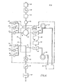
- Fig. 4 there is shown the gas supply and exhaust system for each module 13. It should be noted that the system is duplicated for each module 13 in a console.
- Tube 41 connects the chamber within process module 21 embodiment, tube 41 is connected to three incoming lines 43, 44 and 45 via flow controllers 46, 47 and 48 which may be of the type as disclosed in U.S. Patent Application entitled “Molar Gas- Flow Controller", Serial No. ------- filed ----- and assigned to the same assignee as the present application. Any one or combination of gas sources may be connected to process module 21 to deliver etching gases to process module 21 in desired percentages.
- Gas in process module 21 is converted to a plasma, i.e., ionized by connecting an R F source of voltage 49 to electrodes 21c and 21d of process module 21.
- Exit tube 42 is connected to exhaust the gas to atmosphere via cold trap.50, shut-off valve 51, throttle valve 52 and pump 53.
- the load module 20 receives gases from one or more sources.
- the tabe -1 of load module 20 is connected to three input tubes 54, 55 and 56 via flow controllers 57, 58 and 59, which functions in a manner similar to flow controllers 46, 47 and 48 to introduce one or more gases to load module in selectable percentages.
- Gas from load module 20 is exhausted via shut-off valve 60, throttle valve 61 and pump 6Z in a manner similar to that described above in connection with process module 21, i.e., throttle 61 controls the rate of gas exhaustion by pump 62 and therefore pressure within load module 20.
- the process module 21 and load module 20 are each monitored by pressure gages 63 and 64, respectively.
- the pressure gages 63 and 64 must be sensitive enough to measure pressures one Torr or below which is the vacuum range at which it is necessary to keep the load module 20 and process module 21 within during pretreating, stripping and etching. In this way the system may be monitored to assure that pressure within each module is within pressure tolerances before a process step is carried out.
- capacitance manometers which are highly sensitive at very low pressures are used.
- Capacitance manometers 63 and 64 are normally connected to process module 21 and load module 20, respectively, through valves 65 and 66.
- each is zeroed from time to time, e.g., after each etching operation by connecting capacitance manometers 63 and 64 to diffusion pumps 67 and 68 for a brief time by switching valve 65 and 66 to diffusion pumps 67 and 68, respectively.
- Diffusion pumps 67 and 68 produce a pressure that is less than the lowest pressure that will produce a response on a capacitance manometer.
- the reading of a capacitance manometer connected to a diffusion pump is the correction factor which must be subtracted from readings when the capacitance manometer is connected back to the process module,21 or load module 20.
- a roughing pump 69 is connected to each of diffusion pumps 67 and 68 and is used to bring the pressure in diffusion pumps 67 and 68 to their operative pressures prior to connection to capacitance manometers 63 and 64.
- This arrangement is more fully set forth in U.S. Application entitled “Auto-Zero System For Pressure Transducer", Serial No. 203,735 filed November 3, 1980, having the same assignee as the present application.
- the present invention may be operated manually or under the control of a microprocessor.
- a microprocessor may operate manually or under the control of a microprocessor.
- a unique wafer processing apparatus wherein a first wafer is etched while a second wafer is being pretreated or stripped.
- a wafer once a wafer enters the module 31 for processing, it doesn't see atmosphere until it is pretreated, etched and stripped.
Landscapes
- Chemical & Material Sciences (AREA)
- Analytical Chemistry (AREA)
- Drying Of Semiconductors (AREA)
- ing And Chemical Polishing (AREA)
- Exposure Of Semiconductors, Excluding Electron Or Ion Beam Exposure (AREA)
Applications Claiming Priority (2)
| Application Number | Priority Date | Filing Date | Title |
|---|---|---|---|
| US06/219,060 US4341582A (en) | 1980-12-22 | 1980-12-22 | Load-lock vacuum chamber |
| US219060 | 1980-12-22 |
Publications (3)
| Publication Number | Publication Date |
|---|---|
| EP0060917A2 true EP0060917A2 (fr) | 1982-09-29 |
| EP0060917A3 EP0060917A3 (en) | 1983-04-06 |
| EP0060917B1 EP0060917B1 (fr) | 1987-03-11 |
Family
ID=22817684
Family Applications (1)
| Application Number | Title | Priority Date | Filing Date |
|---|---|---|---|
| EP81108149A Expired EP0060917B1 (fr) | 1980-12-22 | 1981-10-09 | Chambre à vide pour le décapage de silicium munie d'un système de chargement et de serrure |
Country Status (5)
| Country | Link |
|---|---|
| US (1) | US4341582A (fr) |
| EP (1) | EP0060917B1 (fr) |
| JP (1) | JPS57128928A (fr) |
| CA (1) | CA1171551A (fr) |
| DE (1) | DE3175990D1 (fr) |
Cited By (2)
| Publication number | Priority date | Publication date | Assignee | Title |
|---|---|---|---|---|
| EP0272140A3 (en) * | 1986-12-19 | 1990-11-14 | Applied Materials, Inc. | Thermal cvd/pecvd reactor and use for thermal chemical vapor deposition of silicon dioxide and in-situ multi-step planarized process |
| EP0416646A3 (en) * | 1989-09-08 | 1991-08-28 | Tokyo Electron Limited | Apparatus and method for processing substrates |
Families Citing this family (32)
| Publication number | Priority date | Publication date | Assignee | Title |
|---|---|---|---|---|
| US4484809B1 (en) * | 1977-12-05 | 1995-04-18 | Plasma Physics Corp | Glow discharge method and apparatus and photoreceptor devices made therewith |
| JPS5816078A (ja) * | 1981-07-17 | 1983-01-29 | Toshiba Corp | プラズマエツチング装置 |
| USD275032S (en) | 1982-01-06 | 1984-08-07 | Drytek, Inc. | Plasma cassette etcher |
| US4381965A (en) * | 1982-01-06 | 1983-05-03 | Drytek, Inc. | Multi-planar electrode plasma etching |
| NL8300220A (nl) * | 1983-01-21 | 1984-08-16 | Philips Nv | Inrichting voor het stralingslithografisch behandelen van een dun substraat. |
| JPH0666298B2 (ja) * | 1983-02-03 | 1994-08-24 | 日電アネルバ株式会社 | ドライエッチング装置 |
| US4584045A (en) * | 1984-02-21 | 1986-04-22 | Plasma-Therm, Inc. | Apparatus for conveying a semiconductor wafer |
| US4547247A (en) * | 1984-03-09 | 1985-10-15 | Tegal Corporation | Plasma reactor chuck assembly |
| US4657620A (en) * | 1984-10-22 | 1987-04-14 | Texas Instruments Incorporated | Automated single slice powered load lock plasma reactor |
| US4657617A (en) * | 1984-10-22 | 1987-04-14 | Texas Instruments Incorporated | Anodized aluminum substrate for plasma etch reactor |
| US4657618A (en) * | 1984-10-22 | 1987-04-14 | Texas Instruments Incorporated | Powered load lock electrode/substrate assembly including robot arm, optimized for plasma process uniformity and rate |
| US4654106A (en) * | 1984-10-22 | 1987-03-31 | Texas Instruments Incorporated | Automated plasma reactor |
| US4661196A (en) * | 1984-10-22 | 1987-04-28 | Texas Instruments Incorporated | Plasma etch movable substrate |
| US4657621A (en) * | 1984-10-22 | 1987-04-14 | Texas Instruments Incorporated | Low particulate vacuum chamber input/output valve |
| US4659413A (en) * | 1984-10-24 | 1987-04-21 | Texas Instruments Incorporated | Automated single slice cassette load lock plasma reactor |
| US4915917A (en) * | 1987-02-19 | 1990-04-10 | The Johns Hopkins University | Glow discharge unit |
| JP2501444B2 (ja) * | 1987-03-19 | 1996-05-29 | 東京エレクトロン株式会社 | アツシング装置 |
| US4861563A (en) * | 1987-05-14 | 1989-08-29 | Spectrum Cvd, Inc. | Vacuum load lock |
| US4923584A (en) * | 1988-10-31 | 1990-05-08 | Eaton Corporation | Sealing apparatus for a vacuum processing system |
| US5227000A (en) * | 1990-04-09 | 1993-07-13 | Nippon Scientific Co., Ltd. | Plasma etching apparatus with accurate temperature and voltage level control on device under test |
| US6095083A (en) * | 1991-06-27 | 2000-08-01 | Applied Materiels, Inc. | Vacuum processing chamber having multi-mode access |
| US6672819B1 (en) | 1995-07-19 | 2004-01-06 | Hitachi, Ltd. | Vacuum processing apparatus and semiconductor manufacturing line using the same |
| JPH0936198A (ja) | 1995-07-19 | 1997-02-07 | Hitachi Ltd | 真空処理装置およびそれを用いた半導体製造ライン |
| DE19629094C2 (de) * | 1995-07-28 | 2000-07-27 | Matsushita Electric Industrial Co Ltd | Gerät und Verfahren zur Drahtkontaktierung unter Verwendung des Oberflächenbehandlungsgerätes |
| DE19654975C2 (de) * | 1995-07-28 | 2002-07-25 | Matsushita Electric Industrial Co Ltd | Gerät und Verfahren zur Oberflächenbehandlung |
| JP3353746B2 (ja) | 1999-07-06 | 2002-12-03 | 松下電器産業株式会社 | 表面処理装置 |
| US6528435B1 (en) * | 2000-08-25 | 2003-03-04 | Wafermasters, Inc. | Plasma processing |
| US6609877B1 (en) * | 2000-10-04 | 2003-08-26 | The Boc Group, Inc. | Vacuum chamber load lock structure and article transport mechanism |
| TW511215B (en) * | 2001-10-15 | 2002-11-21 | Macronix Int Co Ltd | Inspection method for dynamic particle contaminant state of the etching chamber |
| US6719517B2 (en) * | 2001-12-04 | 2004-04-13 | Brooks Automation | Substrate processing apparatus with independently configurable integral load locks |
| US6962644B2 (en) * | 2002-03-18 | 2005-11-08 | Applied Materials, Inc. | Tandem etch chamber plasma processing system |
| TW201330086A (zh) * | 2012-01-05 | 2013-07-16 | Duan-Ren Yu | 蝕刻裝置 |
Family Cites Families (6)
| Publication number | Priority date | Publication date | Assignee | Title |
|---|---|---|---|---|
| JPS5291650A (en) * | 1976-01-29 | 1977-08-02 | Toshiba Corp | Continuous gas plasma etching apparatus |
| JPS5421175A (en) * | 1977-07-18 | 1979-02-17 | Tokyo Ouka Kougiyou Kk | Improvement of plasma reaction processor |
| US4208159A (en) * | 1977-07-18 | 1980-06-17 | Tokyo Ohka Kogyo Kabushiki Kaisha | Apparatus for the treatment of a wafer by plasma reaction |
| JPS5487477A (en) * | 1977-12-23 | 1979-07-11 | Kokusai Electric Co Ltd | Device for etching and stripping semiconductor wafer |
| JPS5588335A (en) * | 1978-12-07 | 1980-07-04 | Kokusai Electric Co Ltd | Automatic conveying mechanism for plasma etching/ stripping device |
| US4209357A (en) * | 1979-05-18 | 1980-06-24 | Tegal Corporation | Plasma reactor apparatus |
-
1980
- 1980-12-22 US US06/219,060 patent/US4341582A/en not_active Expired - Lifetime
-
1981
- 1981-10-01 CA CA000387129A patent/CA1171551A/fr not_active Expired
- 1981-10-09 EP EP81108149A patent/EP0060917B1/fr not_active Expired
- 1981-10-09 DE DE8181108149T patent/DE3175990D1/de not_active Expired
- 1981-12-21 JP JP56205352A patent/JPS57128928A/ja active Pending
Cited By (4)
| Publication number | Priority date | Publication date | Assignee | Title |
|---|---|---|---|---|
| EP0272140A3 (en) * | 1986-12-19 | 1990-11-14 | Applied Materials, Inc. | Thermal cvd/pecvd reactor and use for thermal chemical vapor deposition of silicon dioxide and in-situ multi-step planarized process |
| US6167834B1 (en) | 1986-12-19 | 2001-01-02 | Applied Materials, Inc. | Thermal CVD/PECVD reactor and use for thermal chemical vapor deposition of silicon dioxide and in-situ multi-step planarized process |
| EP0416646A3 (en) * | 1989-09-08 | 1991-08-28 | Tokyo Electron Limited | Apparatus and method for processing substrates |
| US5164034A (en) * | 1989-09-08 | 1992-11-17 | Tokyo Electron Limited | Apparatus and method for processing substrate |
Also Published As
| Publication number | Publication date |
|---|---|
| JPS57128928A (en) | 1982-08-10 |
| CA1171551A (fr) | 1984-07-24 |
| EP0060917B1 (fr) | 1987-03-11 |
| US4341582A (en) | 1982-07-27 |
| EP0060917A3 (en) | 1983-04-06 |
| DE3175990D1 (en) | 1987-04-16 |
Similar Documents
| Publication | Publication Date | Title |
|---|---|---|
| US4341582A (en) | Load-lock vacuum chamber | |
| US5562800A (en) | Wafer transport method | |
| US5858878A (en) | Semiconductor wafer etching method and post-etching process | |
| JP3644036B2 (ja) | 半導体装置の製造方法および半導体製造装置 | |
| CN101236893B (zh) | 基板处理方法和基板处理装置 | |
| US5628828A (en) | Processing method and equipment for processing a semiconductor device having holder/carrier with flattened surface | |
| US20020197145A1 (en) | Substrate processing apparatus and a method for fabricating a semiconductor device by using same | |
| JPH08291384A (ja) | 圧力調整装置及びこれを用いた部屋の連通方法 | |
| KR20040047303A (ko) | 기판 이송 모듈의 오염을 제어할 수 있는 기판 처리 장치및 방법 | |
| JPH10303279A (ja) | 真空処理装置 | |
| JPH07211761A (ja) | 処理装置内の被処理体の搬送方法 | |
| KR100739969B1 (ko) | 도포 현상 처리 방법 및 도포 현상 처리 시스템 | |
| JPH06151561A (ja) | 基板保持装置、並びにこれを用いた露光装置と半導体デバイス製造方法 | |
| JPH05251408A (ja) | 半導体ウェーハのエッチング装置 | |
| JP3253002B2 (ja) | 処理装置 | |
| JPH05304197A (ja) | マルチチャンバシステム | |
| US20070175395A1 (en) | Semiconductor device manufacturing equipment including a vacuum apparatus and a method of operating the same | |
| TWI875899B (zh) | 用於管理基板釋氣的系統和方法 | |
| JP3153323B2 (ja) | 気密室の常圧復帰装置及びその常圧復帰方法 | |
| US6406553B1 (en) | Method to reduce contaminants from semiconductor wafers | |
| JPH06302557A (ja) | ドライエッチング装置 | |
| JP2735231B2 (ja) | 半導体製造装置 | |
| US6990173B1 (en) | Positioning apparatus, atmosphere substituting method, exposure apparatus, and device manufacturing method | |
| KR20030001095A (ko) | 챔버 설비의 압력 조절 장치 | |
| JPH0536618A (ja) | 半導体製造装置 |
Legal Events
| Date | Code | Title | Description |
|---|---|---|---|
| PUAI | Public reference made under article 153(3) epc to a published international application that has entered the european phase |
Free format text: ORIGINAL CODE: 0009012 |
|
| AK | Designated contracting states |
Designated state(s): CH DE FR GB IT NL |
|
| PUAL | Search report despatched |
Free format text: ORIGINAL CODE: 0009013 |
|
| AK | Designated contracting states |
Designated state(s): CH DE FR GB IT LI NL |
|
| 17P | Request for examination filed |
Effective date: 19831005 |
|
| GRAA | (expected) grant |
Free format text: ORIGINAL CODE: 0009210 |
|
| AK | Designated contracting states |
Kind code of ref document: B1 Designated state(s): CH DE FR GB IT LI NL |
|
| ITF | It: translation for a ep patent filed | ||
| REF | Corresponds to: |
Ref document number: 3175990 Country of ref document: DE Date of ref document: 19870416 |
|
| ET | Fr: translation filed | ||
| PLBE | No opposition filed within time limit |
Free format text: ORIGINAL CODE: 0009261 |
|
| STAA | Information on the status of an ep patent application or granted ep patent |
Free format text: STATUS: NO OPPOSITION FILED WITHIN TIME LIMIT |
|
| 26N | No opposition filed | ||
| PGFP | Annual fee paid to national office [announced via postgrant information from national office to epo] |
Ref country code: FR Payment date: 19911007 Year of fee payment: 11 |
|
| PGFP | Annual fee paid to national office [announced via postgrant information from national office to epo] |
Ref country code: GB Payment date: 19911015 Year of fee payment: 11 Ref country code: CH Payment date: 19911015 Year of fee payment: 11 |
|
| PGFP | Annual fee paid to national office [announced via postgrant information from national office to epo] |
Ref country code: DE Payment date: 19911021 Year of fee payment: 11 |
|
| ITTA | It: last paid annual fee | ||
| PGFP | Annual fee paid to national office [announced via postgrant information from national office to epo] |
Ref country code: NL Payment date: 19911031 Year of fee payment: 11 |
|
| PG25 | Lapsed in a contracting state [announced via postgrant information from national office to epo] |
Ref country code: GB Effective date: 19921009 |
|
| PG25 | Lapsed in a contracting state [announced via postgrant information from national office to epo] |
Ref country code: LI Effective date: 19921031 Ref country code: CH Effective date: 19921031 |
|
| PG25 | Lapsed in a contracting state [announced via postgrant information from national office to epo] |
Ref country code: NL Effective date: 19930501 |
|
| GBPC | Gb: european patent ceased through non-payment of renewal fee |
Effective date: 19921009 |
|
| NLV4 | Nl: lapsed or anulled due to non-payment of the annual fee | ||
| PG25 | Lapsed in a contracting state [announced via postgrant information from national office to epo] |
Ref country code: FR Effective date: 19930630 |
|
| REG | Reference to a national code |
Ref country code: CH Ref legal event code: PL |
|
| PG25 | Lapsed in a contracting state [announced via postgrant information from national office to epo] |
Ref country code: DE Effective date: 19930701 |
|
| REG | Reference to a national code |
Ref country code: FR Ref legal event code: ST |