EP0061213A1 - Anordnung zur Darstellung digitaler Daten, einschliesslich der Auswahl von Bildseiten und/oder der Verbesserung des Auflösungsvermögens - Google Patents
Anordnung zur Darstellung digitaler Daten, einschliesslich der Auswahl von Bildseiten und/oder der Verbesserung des Auflösungsvermögens Download PDFInfo
- Publication number
- EP0061213A1 EP0061213A1 EP82200241A EP82200241A EP0061213A1 EP 0061213 A1 EP0061213 A1 EP 0061213A1 EP 82200241 A EP82200241 A EP 82200241A EP 82200241 A EP82200241 A EP 82200241A EP 0061213 A1 EP0061213 A1 EP 0061213A1
- Authority
- EP
- European Patent Office
- Prior art keywords
- control signal
- control
- pixel
- displayed
- bits
- Prior art date
- Legal status (The legal status is an assumption and is not a legal conclusion. Google has not performed a legal analysis and makes no representation as to the accuracy of the status listed.)
- Granted
Links
- 239000003086 colorant Substances 0.000 abstract description 9
- 230000001360 synchronised effect Effects 0.000 description 5
- 230000000903 blocking effect Effects 0.000 description 2
- 238000012986 modification Methods 0.000 description 2
- 230000004048 modification Effects 0.000 description 2
- 238000000034 method Methods 0.000 description 1
- 230000002093 peripheral effect Effects 0.000 description 1
- 230000003068 static effect Effects 0.000 description 1
Images


Classifications
-
- G—PHYSICS
- G09—EDUCATION; CRYPTOGRAPHY; DISPLAY; ADVERTISING; SEALS
- G09G—ARRANGEMENTS OR CIRCUITS FOR CONTROL OF INDICATING DEVICES USING STATIC MEANS TO PRESENT VARIABLE INFORMATION
- G09G5/00—Control arrangements or circuits for visual indicators common to cathode-ray tube indicators and other visual indicators
- G09G5/02—Control arrangements or circuits for visual indicators common to cathode-ray tube indicators and other visual indicators characterised by the way in which colour is displayed
- G09G5/06—Control arrangements or circuits for visual indicators common to cathode-ray tube indicators and other visual indicators characterised by the way in which colour is displayed using colour palettes, e.g. look-up tables
Definitions
- the invention relates to a device for displaying digital information as a set of pixels which are arranged according to a line pattern in a two-dimensional area, comprising a display memory for the storage of the display information, the information containing m bits for each pixel (m > 1), a data output of said display memory being connected to an address input of a programmable colour map memory which comprises a data output for colour information.
- a device of this kind is known from British Patent Application No. 2,032,740.
- the display memory and the colour map memory of this device are controlled by means of a processor.
- a pixel on the screen of a display apparatus connected to the data output of the colour map memory is formed by an m-bit data word from the display memory.
- This data word indicates an address in the colour map memory.
- a selected colour is programmed, with the result that the pixel is displayed on the display apparatus in the selected colour.
- Suitable programming of the colour map memory enables the display apparatus to display the colour information which is identified by only one or some of the m bits of the pixel.
- this technique is referred to as picture page selection. Each picture page thus produced then has a depth of one or more bits.
- the invention has for its object to provide a device in which picture page selection is achieved without the colour map memory being reprogrammed for each page selected. It is another object of the invention to realize resolution enhancement by means of the same device.
- a device in accordance with the invention is characterized in that at least one connection between the data output of the display memory and the address input of the colour map memory is provided with a gate circuit with a control input for passing, under the control of a first control signal, the m bits of the pixel to be displayed as a first address for the colour map memory and for passing, under the control of a second control signal, a selectable part of the m bits of the pixel to be displayed as a second address for the colour map memory.
- a preferred embodiment of the device in accordance with the invention is characterized in that for each parallel connection the gate circuit comprises at least one logic gate whose control input is connected to a control signal generator for passing, under the control of the second control signal, a first selectable part of the m bits of the pixel to be displayed and for passing, under the control of a third control signal, a second selectable part of the m bits of the pixel to be displayed, the first selectable part and the second selectable part being mutually exclusive.
- control signals generated by the control signal generator indicate which picture page (pages) is (are) displayed and/or which resolution enhancement is realized by the second and the third control signals.
- a preferred embodiment of a device in accordance with the invention is characterized in that said control signals are invariable, during the duration of a picture to be displayed, for the display, under the control of the first control signal, of a first page having a data content of m bits per pixel, and for the display, under the control of the second control signal of at least one second page having a data content of b bits per pixel, b being smaller than m.
- Another embodiment of a device in accordance with the invention is characterized in that said second and third control signals for a parallel connection of m logic gates, one gate being provided for each connection, are in phase with the period in which a pixel is presented to said parallel connection, said period comprising at least two non-overlapping subperiods, the second control signal being active only during a first subperiod and the third control signal being active only during a second subperiod.
- a further preferred embodiment .of a device in accordance with the invention is characterized in that said second and third control signals for a first parallel connection of m logic gates, one gate being provided for each connection, are in phase with the frame period of a frame pattern, the second control signal being active only during the period of a first frame and the third control signal being active only during the period of a second frame.
- the gate circuit comprises at least one second parallel connection of m logic gates, said first and said second parallel connections being connected in series, a fourth and a fifth control signal for the second parallel connection being in phase with the period in which a pixel is presented to the second parallel connection, said period comprising at least two non-overlapping subperiods, the fourth control signal being active only during the first subperiod and the fifth control signal being active only during a second subperiod in order to pass, under the control of the fourth control signal, a third selectable part of the m bits of the pixel to be displayed and in order to pass, under the control of the fifth control signal, a fourth selectable part of the m bits, said third and fourth selectable parts being mutually exclusive.
- the gate circuit comprises at least one second parallel connection of m logic gates, said first and said second parallel connections being connected in series, a fourth and a fifth control signal for the second parallel connection being in phase with the period in which a pixel is presented to the second parallel connection, said period comprising at least two non-overlapping sub
- control signal generator is a memory which can be addressed in phase with the period in which a pixel is presented to the gate circuit and/or with the period of a frame pattern in order to generate second and third control signals during these periods.
- the reference numeral 1 denotes a display memory for the storage of information to be displayed; the reference numerals 3, 4 and 5 denote digital-to-analog converters.
- Element 2 is a colour map memory.
- the colour map memory is controlled by a processor 6 which also controls the display memory 1; element 7 is a display apparatus.
- a pixel on the screen of the display apparatus 7 is stored in the display memory 1 in the form of a data word of m bits.
- the m-bit data word forms an m-bit address which indicates a location in the colour map memory.
- a colour is programmed at this location in the colour map memory.
- 2 m locations in the colour map memory can be indicated, implying 2 m selection possibilities.
- the colour map memory is a random access memory which can be programmed by means of the processor 6.
- the word in the colour map memory has a width of n bits (n > 1), so that a selection from 2 n colours is possible.
- the display memory may be considered to Consist of a maximum of m pages having a depth of 1 bit each.
- a i and b. represent numbers and i is the number of groups of pages.
- Such a page of the i group then has 2 b i colour possibilities.
- a pixel of the display memory comprises five bits, it is possible to display 1 page x 2 bits plus 2 pages x 1 bit on the display apparatus.
- Page selection is obtained in accordance with the state of the art by programming the colour map memory in a special manner.
- the colour map memory is then programmed so that only the bits from the pages to be displayed activate the digital-to-analog converters.
- Figure 2a illustrates the idea of the invention in a device for the display of digital information in which colour possibilities can be exchanged against pages as well as against enhancement of resolution.
- At least one connection between the display memory 1 and the colour map memory 2 in this device comprises a gate circuit.
- the gate circuit comprises at least one logic gate G which has a control input which is connected to a control signal generator 8.
- the control signal generator generates control signals under the influence of which the gate device operates in the passing or the blocking mode.
- the gate circuit is in the passing mode, the data word on the data output of the display memory is the same as the address word applied to the colour map memory.
- Page selection is realized by means of control signals which are statically activated on the control input of the control circuit.
- the control signals can also be dynamically activated, which means that they are in phase with the period in which the pixels are applied to the gate circuit and/or with the period of the frames for frame-wise display; the resolution of the picture to be displayed is then enhanced.
- Figure 2b shows a preferred embodiment of a device in accordance with the invention in which colour possibilities are exchanged against pages, without it being necessary to reprogram the content of the colour map memory 2.
- the elements which correspond to those shown in Figure 1 are denoted by the same reference numerals.
- Each connection in this preferred embodiment comprises a gate circuit between the data output of the picture memory 1 and the address input of the colour map memory, said gate circuit comprising a logic AND-gate ( G ).
- G a logic AND-gate
- PPA peripheral interfate adapter, Motorola MC 6820
- Selection of one or more pages is realized by means of a control signal on the control lines C to C m which is statically activated, static in this respect being understood to mean that the control signal is invariable during the duration of a picture to be displayed.
- a control signal is to be understood to mean herein a set of m signals, one on each control line.
- a selected number of logic AND-gates G(i) changes to the passing mode when such a control signal is applied.
- a selection of another page or pages is simply realized by modification of the content of the buffer 8, so that another control signal having another content is applied to the control lines C 1 to C . In this embodiment the selection of a page is determined by one variable, that is to say the bit value of the control signal on the associated control line C.. In order to establish which page (pages) of the memory is (are) displayed on the screen of the display apparatus 7, it is sufficient to read the content of the buffer 8.
- the data word formed on the output of the parallel connection of logic gates G 1 , ... G m is an address for the colour map memory.
- the colour of the common pixels on the screen of the display apparatus is determined by the content of the colour map memory.
- a picture consists of two mutually perpendicular bars and that the memory is divided into pages, such that for example, the horizontal bar is present on a first page and a second page contains the vertical bar. If only the signal on, for example, the first control line C 1 is high (p1, address 0001) and low on all other control lines, only the first page is displayed. On the screen of the display apparatus 7 a red horizontal bar then appears on a black background. The black background is formed in that all other connection lines carry a low signal, so that the location 0000 (black) of the colour map memory is addressed for the pixels which do not form part of the horizontal bar.
- FIG 4 shows an example of the "overlay" mode. Assume, for example, that the colour map memory is programmed in accordance with the table below.
- the picture consists of three overlapping rectangles, each of which is present on one page of the display memory.
- Priorities can be assigned to given pages by suitable programming of the colour map memory.
- address 0011 signal high on, for example control lines C 1 and C 2
- green is the colour having the highest priority (0010 and 0011), so that a part of the first page (p1, address 0001 f red) is overlapped by the second page (p2, address 0010, green).
- address 0110 is displayed
- blue is the colour having the highest priority (0100 and 0110), so that a part of the green page is overlapped by the blue page.
- blue is the dominant colour (0100 and 0111).
- the device in accordance with the invention can also be used for exchanging colour possibilities against enhancement of resolution.
- the resolution can be enhanced in the horizontal as well as in the vertical direction.
- the enhancement in the vertical direction is limited by the number of TV lines used for the display of one pixel. Usually, one line per frame is used in apparatus operating with a frame pattern.
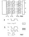
- Figure 5 shows an embodiment of a device for the display of digital information in which colour possibilities are exchanged against doubling of the resolution in the horizontal as well as the vertical direction.
- the data output of the display memory 1 is connected to the address input of the colour map memory 2 via m parallel connections.
- Each connection comprises a first logic AND-gate GH and a second logic AND-gate GV which are connected in series, which means that an output of the first logic AND-gate is connected to an input of the second logic AND-gate.
- All first logic AND-gates GH(1), GH(2), ... GH(m) of all m connections form a first parallel connection and all second logic AND-gates GV(1), GV(2), ... GV(m) form a second parallel connection.
- the doubling of the resolution in the horizontal direction is realized by means of control signals on the control lines 19 and 20.
- the control line 19 is connected to the control inputs of a first half, GH(l) to GH(m/2) of the logicJND-gates of the first parallel connection;
- the control line 20 is connected to the control inputs of a second half, GH (m/2+1) to GH(m), of the logic AND-gates of the first parallel connection. It is assumed that m is an even number. If m is an odd number, a different number of colours exist for the two parts.
- the control lines 19 and 20 are connected to respective outputs of logic NAND-gates 13A and 13B.
- a first input (input A) of the logic NAND-gates 13A and 13B is connected to a connection line 11 which carries a signal ENH (enable horizontal) from the buffer 8.
- ENH encoded horizontal
- the presence of the signal ENH on the connection line 11 activates the doubling of the resolution in the horizontal direction.
- the control signals on the control lines 19 and 20 must be synchronized with the pixel frequency.
- the pixel frequency signal is applied directly to a second input (input B) of the logic NAND-gate 13A via the connection line 17 and, via an inverting gate 15, to a second input of the logic NAND-gate 13B.
- Pixel frequency is to be understood to mean herein the frequency at which the mbits of the pixel to be displayed are applied to the input of" the gate circuit, being the first parallel connection in this embodiment. Because the frequency and the period are related as known from physics, the description can also be given on the basis of the period in which the m bits of the pixel to be displayed are applied to the input of the gate circuit. The control signals for enhancement of the resolution in the horizontal direction must then be in phase with the period.
- the pixel frequency signal is high on a second input (input B) of the gate 13A and during the second half of the period the signal is high on a second input of the gate 13B.
- A "1"
- the gates GH(m/2 + 1) to GH(m) are conductive.
- the location is addressed whose address is composed of m/2 zeroes and m/2 bits of the m-bit data word on the output of the display memory 1 (00...0, xx...x).
- the location having the address composed of the remaining m/2 bits of the m-bit data word and the m/2 zeroes of the colour map memory is then addressed (xx...x, 00...0).
- Figure 6 shows an embodiment of a device for exchanging colour possibilities against a feasible and permissible resolution enhancement.
- the lines S 1 to S 2n are control lines which carry control signals. These control signals are synchronized in time with the pixel frequency or an integer multiple thereof for resolution enhancement in the horizontal direction (suitable frequency signals). For resolution enhancement in the vertical direction, the control signals are synchronized in time with the frame frequency. Resolution enhancement in the vertical direction is limited by the number of TV lines used per frame; therefore, if only two TV lines are used, one for the even and one for the odd frame, the resolution can only be doubled in the vertical direction.
- a multiple of the pixel frequency is obtained, for example, by multiplying the pixel frequency by a suitable factor by means of a multiplier or, if the pixel frequency is derived from a signal of higher frequency, by division of said signal of higher frequency.
- Figure 7 illustrates some examples of resolution enhancement which can be realized by means of a device as shown in Figure 6.
- Figure 8 shows a general solution for the exchange of colour possibilities against resolution and/or pages. Elements which correspond to elements of Figure 2 are denoted by the same reference numerals.
- the element 10 is a memory, for example, a read- only memory or a PLA (programmable logic array).
- the elements 11 and 12 are arithmetic elements, for example, a multiplier or divider which ensure that the pixel frequency signal, or a suitable multiple thereof, and the frame frequency, or a signal derived from the frame frequency, are applied to an input of the memory 10.
- a selection of pages, or the selection from feasible resolution enhancements in the horizontal direction, the vertical direction, or a combination in the horizontal and the vertical direction, is then merely a matter of indicating the appropriate memory address containing the suitable pixel frequency and the frame frequency signal.
- a selected possibility is stored at a given address in the memory 10.
- an address of the memory 10 at which the selected possibility is programmed is addressed.
- a control signal for the logic AND-gates G(1), G(2), ... G(m) is then outputted on the data output of the memory 10.
- the connection lines T(1), T(2), ... T(m) connect the data output of the memory 10 to the second inputs of the logic gates.
- the memory 10 is statically activated, which means that the control signals are independent of the pixel frequency and the frame frequency.
- the associated logic gates G(i) are conductive under the influence of the selected control signal, programmed at the selected address.
- the memory 10 is dynamically activated, which means that the control signals are synchronized with the associated, suitable pixel frequency and/or frame frequency.
Landscapes
- Engineering & Computer Science (AREA)
- Physics & Mathematics (AREA)
- Computer Hardware Design (AREA)
- General Physics & Mathematics (AREA)
- Theoretical Computer Science (AREA)
- Control Of Indicators Other Than Cathode Ray Tubes (AREA)
- Digital Computer Display Output (AREA)
- Controls And Circuits For Display Device (AREA)
Applications Claiming Priority (2)
| Application Number | Priority Date | Filing Date | Title |
|---|---|---|---|
| NL8101339A NL8101339A (nl) | 1981-03-19 | 1981-03-19 | Inrichting voor het afbeelden van digitale informatie met selektiemogelijkheid van beeldpagina's en/of resolutie uitbreiding. |
| NL8101339 | 1981-03-19 |
Publications (2)
| Publication Number | Publication Date |
|---|---|
| EP0061213A1 true EP0061213A1 (de) | 1982-09-29 |
| EP0061213B1 EP0061213B1 (de) | 1985-12-18 |
Family
ID=19837192
Family Applications (1)
| Application Number | Title | Priority Date | Filing Date |
|---|---|---|---|
| EP82200241A Expired EP0061213B1 (de) | 1981-03-19 | 1982-02-26 | Anordnung zur Darstellung digitaler Daten, einschliesslich der Auswahl von Bildseiten und/oder der Verbesserung des Auflösungsvermögens |
Country Status (5)
| Country | Link |
|---|---|
| US (1) | US4500875A (de) |
| EP (1) | EP0061213B1 (de) |
| JP (1) | JPS57167087A (de) |
| DE (1) | DE3267966D1 (de) |
| NL (1) | NL8101339A (de) |
Cited By (9)
| Publication number | Priority date | Publication date | Assignee | Title |
|---|---|---|---|---|
| FR2581779A1 (fr) * | 1985-05-10 | 1986-11-14 | Sintra | Circuit de commande pour machine graphique et utilisation d'un tel circuit dans une machine graphique interactive |
| WO1987007973A1 (en) * | 1986-06-18 | 1987-12-30 | Technology Inc., 64 | A display processor |
| EP0165665A3 (de) * | 1984-04-16 | 1989-02-22 | Texas Instruments Incorporated | Kollisionsdetektor für bewegliche Muster |
| EP0167802A3 (en) * | 1984-06-06 | 1989-06-14 | Hitachi, Ltd. | Character and pattern display system |
| EP0149309A3 (en) * | 1983-11-03 | 1989-07-19 | Unisys Corporation | System for electronically displaying multiple images on a crt screen such that some images are more prominent than others |
| EP0202426A3 (en) * | 1985-04-15 | 1989-08-23 | International Business Machines Corporation | Raster scan digital display system |
| EP0148659A3 (de) * | 1983-11-25 | 1989-10-25 | Sony Corporation | Videoanzeigesteuergerät |
| US4935730A (en) * | 1984-10-16 | 1990-06-19 | Sanyo Electric Co., Ltd. | Display apparatus |
| US5552804A (en) * | 1984-04-16 | 1996-09-03 | Texas Instruments Incorporated | Sprite coincidence detector indicating sprite group |
Families Citing this family (20)
| Publication number | Priority date | Publication date | Assignee | Title |
|---|---|---|---|---|
| EP0121015B1 (de) * | 1983-03-31 | 1990-03-07 | International Business Machines Corporation | Abbildungsraumverwaltung und Wiedergabe in einem bestimmten Teil des Bildschirms eines virtuellen Mehrfunktionsterminals |
| US4574277A (en) * | 1983-08-30 | 1986-03-04 | Zenith Radio Corporation | Selective page disable for a video display |
| JPS6062276A (ja) * | 1983-09-14 | 1985-04-10 | Hitachi Ltd | フルカラ−プリンタ制御回路 |
| JPS6067989A (ja) * | 1983-09-26 | 1985-04-18 | 株式会社日立製作所 | 画像表示装置 |
| US4648049A (en) * | 1984-05-07 | 1987-03-03 | Advanced Micro Devices, Inc. | Rapid graphics bit mapping circuit and method |
| US4677574A (en) * | 1984-08-20 | 1987-06-30 | Cromemco, Inc. | Computer graphics system with low memory enhancement circuit |
| US4704697A (en) * | 1985-06-17 | 1987-11-03 | Counterpoint Computers | Multiple station video memory |
| US4887968A (en) * | 1985-12-13 | 1989-12-19 | The Ohio Art Company | Electronic sketching device |
| US4764763A (en) * | 1985-12-13 | 1988-08-16 | The Ohio Art Company | Electronic sketching device |
| GB8614876D0 (en) * | 1986-06-18 | 1986-07-23 | Rca Corp | Display processors |
| US4783652A (en) * | 1986-08-25 | 1988-11-08 | International Business Machines Corporation | Raster display controller with variable spatial resolution and pixel data depth |
| US5109348A (en) * | 1987-09-14 | 1992-04-28 | Visual Information Technologies, Inc. | High speed image processing computer |
| US5146592A (en) * | 1987-09-14 | 1992-09-08 | Visual Information Technologies, Inc. | High speed image processing computer with overlapping windows-div |
| US4985848A (en) * | 1987-09-14 | 1991-01-15 | Visual Information Technologies, Inc. | High speed image processing system using separate data processor and address generator |
| US5129060A (en) * | 1987-09-14 | 1992-07-07 | Visual Information Technologies, Inc. | High speed image processing computer |
| US4991120A (en) * | 1989-05-30 | 1991-02-05 | Eastman Kodak Company | Apparatus for interfacing video frame store with color display device |
| JPH05204350A (ja) * | 1992-01-29 | 1993-08-13 | Sony Corp | 画像データ処理装置 |
| US5970471A (en) | 1996-03-22 | 1999-10-19 | Charles E. Hill & Associates, Inc. | Virtual catalog and product presentation method and apparatus |
| EP1124374A1 (de) * | 2000-02-08 | 2001-08-16 | Koninklijke Philips Electronics N.V. | Teletextempfänger |
| JP5347786B2 (ja) * | 2008-11-18 | 2013-11-20 | セイコーエプソン株式会社 | 画像処理コントローラー、及び、印刷装置 |
Citations (2)
| Publication number | Priority date | Publication date | Assignee | Title |
|---|---|---|---|---|
| FR2411446A1 (fr) * | 1977-12-09 | 1979-07-06 | Ibm | Systeme d'affichage de caracteres graphiques en couleur |
| GB2032740A (en) * | 1978-10-16 | 1980-05-08 | Tektronix Inc | Programmable color mapping |
Family Cites Families (3)
| Publication number | Priority date | Publication date | Assignee | Title |
|---|---|---|---|---|
| JPH0153555B2 (de) * | 1978-03-13 | 1989-11-14 | Rca Licensing Corp | |
| DE2847390A1 (de) * | 1978-11-02 | 1980-05-08 | Hartmann & Braun Ag | Verfahren zur darstellung mehrfarbiger zeichen auf dem bildschirm eines datensichtgeraetes |
| US4232311A (en) * | 1979-03-20 | 1980-11-04 | Chyron Corporation | Color display apparatus |
-
1981
- 1981-03-19 NL NL8101339A patent/NL8101339A/nl not_active Application Discontinuation
-
1982
- 1982-02-08 US US06/346,702 patent/US4500875A/en not_active Expired - Lifetime
- 1982-02-26 EP EP82200241A patent/EP0061213B1/de not_active Expired
- 1982-02-26 DE DE8282200241T patent/DE3267966D1/de not_active Expired
- 1982-03-19 JP JP57043013A patent/JPS57167087A/ja active Granted
Patent Citations (2)
| Publication number | Priority date | Publication date | Assignee | Title |
|---|---|---|---|---|
| FR2411446A1 (fr) * | 1977-12-09 | 1979-07-06 | Ibm | Systeme d'affichage de caracteres graphiques en couleur |
| GB2032740A (en) * | 1978-10-16 | 1980-05-08 | Tektronix Inc | Programmable color mapping |
Non-Patent Citations (1)
| Title |
|---|
| ISA TRANSACTIONS, vol.19, no.2, 1980, Pittsburgh (US) * |
Cited By (10)
| Publication number | Priority date | Publication date | Assignee | Title |
|---|---|---|---|---|
| EP0149309A3 (en) * | 1983-11-03 | 1989-07-19 | Unisys Corporation | System for electronically displaying multiple images on a crt screen such that some images are more prominent than others |
| EP0148659A3 (de) * | 1983-11-25 | 1989-10-25 | Sony Corporation | Videoanzeigesteuergerät |
| EP0165665A3 (de) * | 1984-04-16 | 1989-02-22 | Texas Instruments Incorporated | Kollisionsdetektor für bewegliche Muster |
| US5552804A (en) * | 1984-04-16 | 1996-09-03 | Texas Instruments Incorporated | Sprite coincidence detector indicating sprite group |
| EP0167802A3 (en) * | 1984-06-06 | 1989-06-14 | Hitachi, Ltd. | Character and pattern display system |
| US4935730A (en) * | 1984-10-16 | 1990-06-19 | Sanyo Electric Co., Ltd. | Display apparatus |
| EP0202426A3 (en) * | 1985-04-15 | 1989-08-23 | International Business Machines Corporation | Raster scan digital display system |
| FR2581779A1 (fr) * | 1985-05-10 | 1986-11-14 | Sintra | Circuit de commande pour machine graphique et utilisation d'un tel circuit dans une machine graphique interactive |
| EP0201428A1 (de) * | 1985-05-10 | 1986-12-17 | Thomson-Csf | Steuerungsschaltung für eine graphische Maschine und Verwendung dieser Schaltung in einer interaktiven graphischen Maschine |
| WO1987007973A1 (en) * | 1986-06-18 | 1987-12-30 | Technology Inc., 64 | A display processor |
Also Published As
| Publication number | Publication date |
|---|---|
| EP0061213B1 (de) | 1985-12-18 |
| US4500875A (en) | 1985-02-19 |
| JPS57167087A (en) | 1982-10-14 |
| DE3267966D1 (en) | 1986-01-30 |
| JPH0420191B2 (de) | 1992-03-31 |
| NL8101339A (nl) | 1982-10-18 |
Similar Documents
| Publication | Publication Date | Title |
|---|---|---|
| EP0061213B1 (de) | Anordnung zur Darstellung digitaler Daten, einschliesslich der Auswahl von Bildseiten und/oder der Verbesserung des Auflösungsvermögens | |
| US3771155A (en) | Color display system | |
| US4470042A (en) | System for displaying graphic and alphanumeric data | |
| US4783652A (en) | Raster display controller with variable spatial resolution and pixel data depth | |
| US5142363A (en) | Method and apparatus for scaling interlaced images | |
| US5059962A (en) | Display system | |
| EP0146229B1 (de) | Einrichtung zum Vergrössern von illuminierten Bildelementen bei Kathodenstrahlanzeigeeinheiten | |
| US5068651A (en) | Image display apparatus | |
| US4345243A (en) | Apparatus for generating signals for producing a display of characters | |
| JPH0255975B2 (de) | ||
| EP0206328A2 (de) | Steuergerät für eine nach dem Rasterverfahren arbeitende Anzeigeeinheit | |
| US4533911A (en) | Video display system for displaying symbol-fragments in different orientations | |
| EP0264603B1 (de) | Digitales nach dem Rasterverfahren arbeitendes Anzeigesystem | |
| US6249273B1 (en) | Method of and device for displaying characters with a border | |
| JPS6252874B2 (de) | ||
| US4901062A (en) | Raster scan digital display system | |
| US20010026282A1 (en) | Method and apparatus for pseudo-random noise generation based on variation of intensity and coloration | |
| JPS6250888A (ja) | 表示システム | |
| US3735384A (en) | Circuit arrangement for character display on a television display screen | |
| KR920008274B1 (ko) | 그래픽 시스템의 16/256 컬러 스위칭 장치 | |
| SU1032477A1 (ru) | Устройство дл отображени информации на телевизионном индикаторе | |
| SU1539826A1 (ru) | Устройство дл отображени информации на экране электронно-лучевой трубки | |
| KR100238209B1 (ko) | 라인메모리를 이용한 모자이크 처리장치 | |
| SU1488872A1 (ru) | Устройство для отображения информации на экране электронно-луче- вой трубки 2 | |
| EP0269174A2 (de) | Logischer Schaltkreis zur Erweiterung einfarbiger Bildmuster in Farbe und Video-Prozessor mit einem solchen logischen Schaltkreis |
Legal Events
| Date | Code | Title | Description |
|---|---|---|---|
| PUAI | Public reference made under article 153(3) epc to a published international application that has entered the european phase |
Free format text: ORIGINAL CODE: 0009012 |
|
| 17P | Request for examination filed |
Effective date: 19820226 |
|
| AK | Designated contracting states |
Designated state(s): DE FR GB SE |
|
| GRAA | (expected) grant |
Free format text: ORIGINAL CODE: 0009210 |
|
| AK | Designated contracting states |
Designated state(s): DE FR GB SE |
|
| REF | Corresponds to: |
Ref document number: 3267966 Country of ref document: DE Date of ref document: 19860130 |
|
| ET | Fr: translation filed | ||
| PLBE | No opposition filed within time limit |
Free format text: ORIGINAL CODE: 0009261 |
|
| STAA | Information on the status of an ep patent application or granted ep patent |
Free format text: STATUS: NO OPPOSITION FILED WITHIN TIME LIMIT |
|
| 26N | No opposition filed | ||
| EAL | Se: european patent in force in sweden |
Ref document number: 82200241.6 |
|
| REG | Reference to a national code |
Ref country code: FR Ref legal event code: CD |
|
| REG | Reference to a national code |
Ref country code: FR Ref legal event code: CD |
|
| PGFP | Annual fee paid to national office [announced via postgrant information from national office to epo] |
Ref country code: FR Payment date: 20000222 Year of fee payment: 19 |
|
| PGFP | Annual fee paid to national office [announced via postgrant information from national office to epo] |
Ref country code: SE Payment date: 20000224 Year of fee payment: 19 |
|
| PGFP | Annual fee paid to national office [announced via postgrant information from national office to epo] |
Ref country code: GB Payment date: 20000228 Year of fee payment: 19 |
|
| PGFP | Annual fee paid to national office [announced via postgrant information from national office to epo] |
Ref country code: DE Payment date: 20000419 Year of fee payment: 19 |
|
| PG25 | Lapsed in a contracting state [announced via postgrant information from national office to epo] |
Ref country code: GB Free format text: LAPSE BECAUSE OF NON-PAYMENT OF DUE FEES Effective date: 20010226 |
|
| PG25 | Lapsed in a contracting state [announced via postgrant information from national office to epo] |
Ref country code: SE Free format text: LAPSE BECAUSE OF NON-PAYMENT OF DUE FEES Effective date: 20010227 |
|
| EUG | Se: european patent has lapsed |
Ref document number: 82200241.6 |
|
| GBPC | Gb: european patent ceased through non-payment of renewal fee |
Effective date: 20010226 |
|
| PG25 | Lapsed in a contracting state [announced via postgrant information from national office to epo] |
Ref country code: FR Free format text: LAPSE BECAUSE OF NON-PAYMENT OF DUE FEES Effective date: 20011031 |
|
| REG | Reference to a national code |
Ref country code: FR Ref legal event code: ST |
|
| PG25 | Lapsed in a contracting state [announced via postgrant information from national office to epo] |
Ref country code: DE Free format text: LAPSE BECAUSE OF NON-PAYMENT OF DUE FEES Effective date: 20011201 |