EP0061926A1 - Mehrweg-Lichtventil für elektrooptische Zeilendrucker mit nicht telezentrischen Abbildungssystemen - Google Patents
Mehrweg-Lichtventil für elektrooptische Zeilendrucker mit nicht telezentrischen Abbildungssystemen Download PDFInfo
- Publication number
- EP0061926A1 EP0061926A1 EP82301659A EP82301659A EP0061926A1 EP 0061926 A1 EP0061926 A1 EP 0061926A1 EP 82301659 A EP82301659 A EP 82301659A EP 82301659 A EP82301659 A EP 82301659A EP 0061926 A1 EP0061926 A1 EP 0061926A1
- Authority
- EP
- European Patent Office
- Prior art keywords
- light valve
- electro
- electrodes
- optic element
- multigate
- Prior art date
- Legal status (The legal status is an assumption and is not a legal conclusion. Google has not performed a legal analysis and makes no representation as to the accuracy of the status listed.)
- Granted
Links
- 238000003384 imaging method Methods 0.000 title claims abstract description 29
- 210000001747 pupil Anatomy 0.000 claims abstract description 6
- 230000005855 radiation Effects 0.000 claims abstract 3
- 238000009304 pastoral farming Methods 0.000 claims description 2
- 239000000758 substrate Substances 0.000 claims 4
- 230000005684 electric field Effects 0.000 claims 1
- XUIMIQQOPSSXEZ-UHFFFAOYSA-N Silicon Chemical compound [Si] XUIMIQQOPSSXEZ-UHFFFAOYSA-N 0.000 description 3
- 230000008901 benefit Effects 0.000 description 3
- 230000004044 response Effects 0.000 description 3
- 229910052710 silicon Inorganic materials 0.000 description 3
- 239000010703 silicon Substances 0.000 description 3
- 230000003287 optical effect Effects 0.000 description 2
- 241000417436 Arcotheres Species 0.000 description 1
- 229910003327 LiNbO3 Inorganic materials 0.000 description 1
- 229910012463 LiTaO3 Inorganic materials 0.000 description 1
- 230000004075 alteration Effects 0.000 description 1
- 238000010276 construction Methods 0.000 description 1
- 239000013078 crystal Substances 0.000 description 1
- 238000010586 diagram Methods 0.000 description 1
- 210000000887 face Anatomy 0.000 description 1
- 230000003993 interaction Effects 0.000 description 1
- 238000000059 patterning Methods 0.000 description 1
- 238000011144 upstream manufacturing Methods 0.000 description 1
Images


Classifications
-
- G—PHYSICS
- G02—OPTICS
- G02F—OPTICAL DEVICES OR ARRANGEMENTS FOR THE CONTROL OF LIGHT BY MODIFICATION OF THE OPTICAL PROPERTIES OF THE MEDIA OF THE ELEMENTS INVOLVED THEREIN; NON-LINEAR OPTICS; FREQUENCY-CHANGING OF LIGHT; OPTICAL LOGIC ELEMENTS; OPTICAL ANALOGUE/DIGITAL CONVERTERS
- G02F1/00—Devices or arrangements for the control of the intensity, colour, phase, polarisation or direction of light arriving from an independent light source, e.g. switching, gating or modulating; Non-linear optics
- G02F1/29—Devices or arrangements for the control of the intensity, colour, phase, polarisation or direction of light arriving from an independent light source, e.g. switching, gating or modulating; Non-linear optics for the control of the position or the direction of light beams, i.e. deflection
- G02F1/31—Digital deflection, i.e. optical switching
- G02F1/315—Digital deflection, i.e. optical switching based on the use of controlled internal reflection
-
- G—PHYSICS
- G02—OPTICS
- G02F—OPTICAL DEVICES OR ARRANGEMENTS FOR THE CONTROL OF LIGHT BY MODIFICATION OF THE OPTICAL PROPERTIES OF THE MEDIA OF THE ELEMENTS INVOLVED THEREIN; NON-LINEAR OPTICS; FREQUENCY-CHANGING OF LIGHT; OPTICAL LOGIC ELEMENTS; OPTICAL ANALOGUE/DIGITAL CONVERTERS
- G02F1/00—Devices or arrangements for the control of the intensity, colour, phase, polarisation or direction of light arriving from an independent light source, e.g. switching, gating or modulating; Non-linear optics
- G02F1/01—Devices or arrangements for the control of the intensity, colour, phase, polarisation or direction of light arriving from an independent light source, e.g. switching, gating or modulating; Non-linear optics for the control of the intensity, phase, polarisation or colour
- G02F1/03—Devices or arrangements for the control of the intensity, colour, phase, polarisation or direction of light arriving from an independent light source, e.g. switching, gating or modulating; Non-linear optics for the control of the intensity, phase, polarisation or colour based on ceramics or electro-optical crystals, e.g. exhibiting Pockels effect or Kerr effect
- G02F1/0305—Constructional arrangements
- G02F1/0316—Electrodes
Definitions
- This invention relates to multigate light valves and, more particularly, to electro-optic line printers and the like having non-telecentric imaging systems.
- an electro-optic element having a plurality of individually addressable electrodes may be employed as a multigate light valve in, say, an electro-optic line printer. See, “Light Gates Give Data Recorder Improved Hardcopy Resolution,” Electronic Design, July 19 1979, pp. 31-32; “Polarizing Filters Plot Analog Waveforms,” Machine Design, Vol. 51, No. 17, July 26 1979, p. 62; and “Data Recorder Eliminates Problem of Linearity,” Design News, February 4 1980, pp. 56-57.
- the zero order diffracted components of the light emerging therefrom are brought to focus at the center of the entrance pupil of an imaging lens (hereinafter simply referred to as the center of the imaging lens) which, in turn, images the light valve onto the recording medium.
- the zero order components of the output beam arc collected as the principal rays for imaging. This ensures that substantially the same amount of light is collected from each of the many electrode pairs of the electro-optic element and that more or less uniform imaging conditions arc maintained across essentially the full width of the light valve.
- a multigate light valvc having converging electrodes is illuminated by a light beam which converges toward the center of the entrance pupil of an imaging lens.
- the electrodes and the light beam converge toward that point at substantially the same angle of convergence so that the light beam effectively remains longitudinally parallel to the electrodes as it passes through the electro-optic element of the light valve.
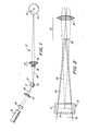
- the recording medium 13 is a photoconductively coated drum 14 which is rotated (by means not shown) in the direction of the arrow.
- the recording medium 13 should be visualized as being a photosensitive medium which is exposed while advancing in a cross line or line pitch direction relative to the light valve 12.
- the light valve 12 comprises an optically transparent electro-optic element 17 and a plurality of individually addressable electrodes 18a-18i.
- the most promising electro-optic matcrials for such a device presently appear to be LiNbO 3 and LiTaO 3 , but there are others which warrant consideration, including BSN, KDP, KD x P, Ba 2 NaNb 5 O 15 and PLZT.
- the light valve 12 is operated in a Total Internal Reflection (TIR) mode. Consequently, the electro-optic clement 17 is suitably a y-cut crystal of, say, LiNb0 3 having an optically polished reflecting surface 21 extending between opposed, optically polishcd input and output faces 22 and 23, respectively.
- the line printer 11 includes a laser 31 or similar source for supplying an input light bearn 32 and a beam expander 33 for laterally expanding the input beam 32 so that it illuminates substantially the full width of the electro-optic element 17.
- the input beam 32 is transmitted through the input face 22 of the electro-optic clement 17 at a grazing angle of incidence relative to the reflecting surface 21 (i.e., an angle no greater than the critical angle of incidence for total internal reflectance frum the surface 21) and is brought to a wedge shaped focus on that surface approximately midway through the electro-optic element 17. Consequently. the input beam 32 is totally internally reflected from the rcflccting surface 21 to provide an output beam 34 which cxits from the electro-optic element 17 through its output face 23.
- the input beam 32 is applied to the electro-optic element 17 through one or more lenses 35 which are selected to have different focal powers laterally and longitudinally of the light valve 12. More particularly, the longitudinal focal power of the lenses 35 (i.e., the focal power along the optical axis of the light valve 12) is selected so that the input beam 32 is brought to a wedge shaped focus on the reflecting surface 21, as previously indicated. On the other hand, the lateral focal power of the lenses 35 is selected so that the input beam 32 converges with a predetermined angle of convergence toward the center of the imaging lens 36.
- the longitudinal focal power of the lenses 35 i.e., the focal power along the optical axis of the light valve 12
- the lateral focal power of the lenses 35 is selected so that the input beam 32 converges with a predetermined angle of convergence toward the center of the imaging lens 36.
- the electrodes 18a-18i are more or less uniformly distributed in spaced apart relationship across essentially the full width of the electro-optic element 17 and arc oriented to longitudinally converge toward the center of the imaging lens 36 with substantially the same angle of convergence as the input beam 32.
- the phase front of the output beam 34 is spatially modulated in accordance with the differentially encoded data samples appearing on the electrodes 18a-18i at any given point in time.
- Schlicren central dark field or bright field imaging optics arc employed to convert the spatial phase front modulation of the output beam 34 into a correspondingly modulated intensity profile and to supply any magnification needed to obtain an image of the desired size on the recording medium 13.
- there arc central dark field imaging optics 37 comprising the imaging lens 36 and a stop 38.
- the stop 38 is centered on the entrance pupil of the imaging lens 36.
- the principal rays of the output beam 34 arc its zero order diffraction components.
- Tnc central dark field character of the imaging optics 37 follows from the fact that the zero order diffraction components of the output beam 34 arc focused on the stop 38. while its higher order diffraction components scatter arnund the stop 38 and arc collected by the imaging lens 36.
- the imaging lens 36 focuses the higher order diffraction components of the output beam 34 on the recording medium 13. thereby providing an intensity modulated image of the light valve 12.
- serial input data samples which represent picture elements for successive lines of an image, arc applied to a differential encoder 41 at a predetermined data rate.
- the encoder 41 differentially encodes the input samples on a line-by-line basis in response to control signals from a controller 42, and a multiplexer 43 responds to further control signals from the controller 42 to ripple the encoded data samples onto the electrodes 18a-18i at a ripple rate which is matched to the data rate.
- the input data may, of course, be buffered (by means not shown) to match the input data rate to any desired ripple rate.
- the input data may be processed (by means also not shown) upstream of the encoder 41 for tcxt editing, formatting or other purposes, provided that the data samples for the ultimate image are applied to the encoder 41 in adjacent picture clement sequence.
- each differentially encoded data samplc other than the first sample for each line of the image, has a magnitude whose difference from the previous diffcrcntially-cncodcd data sample corresponds to the magnitude of a respective input data sample.
- the first sample for each line of the image is referenced to a common reference potential, such as ground.
- the electrodes 18a-18i are supported on or very near its reflecting surface 21.
- the electrodes 18a-18i are defined by suitably patterning a metallised layer of, say, a VLSI silicon circuit 51.
- the silicon circuit 51 is pressed or otherwise firmly held against the electrcroptic clement 17, as indicated by the arrows 52 and 53 ( Figure 3), to maintain the electrodes in contact with or closely adjacent to the reflecting surfacc 21.
- the advantage of this construction is that the silicon circuit 51 may be used to make the neccssary electrical connections to the electrodes 18a- 18i.
- each adjacent pair of electrodes cooperates with the electro-optic element 17 and with the imaging optics 37 to effectively define a local modulator for creating a picture clement at a unique, spatially predetermined position along each line of the image. Since the input data are differentially encoded and all of the electrodes 18a-18i are individually addressable, the number of picture elements that can be printed/scan line is equal to the number of electrodes 18a-18i. Moreover, since the focusing lens or lenses 35 are on the input side of the light valve 12, they contrubute relatively little curvature or distortion to the image.
- the present invention may also be applied to a light valve 61 having a plurality of individually addressable electrodes 62a-62i alternating with a corresponding plurality of reference or ground plane electrodes 63a-63i.
- the major advantage of this cmbodimcnt is that the raw input dataaedircctly applied to the individually addrcssablc electrodes 62a-62i so as to avoid the additional cost and complexity of differential cncoding, and its basic disadvantage is that twice as many electrodes are required to print a given number of picture elements/line.
- this alternative embodiment is otherwise so similar to the embodiment described hcrcinabovc that it need not be described in any further detail. Instead. like reference numerals have been used to identify like parts.
Landscapes
- Physics & Mathematics (AREA)
- Nonlinear Science (AREA)
- General Physics & Mathematics (AREA)
- Optics & Photonics (AREA)
- Chemical & Material Sciences (AREA)
- Engineering & Computer Science (AREA)
- Ceramic Engineering (AREA)
- Crystallography & Structural Chemistry (AREA)
- Printers Or Recording Devices Using Electromagnetic And Radiation Means (AREA)
- Dot-Matrix Printers And Others (AREA)
- Exposure Or Original Feeding In Electrophotography (AREA)
- Mechanical Light Control Or Optical Switches (AREA)
Applications Claiming Priority (2)
| Application Number | Priority Date | Filing Date | Title |
|---|---|---|---|
| US249057 | 1981-03-30 | ||
| US06/249,057 US4413270A (en) | 1981-03-30 | 1981-03-30 | Multigate light valve for electro-optic line printers having non-telecentric imaging systems |
Publications (2)
| Publication Number | Publication Date |
|---|---|
| EP0061926A1 true EP0061926A1 (de) | 1982-10-06 |
| EP0061926B1 EP0061926B1 (de) | 1985-07-10 |
Family
ID=22941878
Family Applications (1)
| Application Number | Title | Priority Date | Filing Date |
|---|---|---|---|
| EP82301659A Expired EP0061926B1 (de) | 1981-03-30 | 1982-03-30 | Mehrweg-Lichtventil für elektrooptische Zeilendrucker mit nicht telezentrischen Abbildungssystemen |
Country Status (5)
| Country | Link |
|---|---|
| US (1) | US4413270A (de) |
| EP (1) | EP0061926B1 (de) |
| JP (1) | JPS57169724A (de) |
| CA (1) | CA1175473A (de) |
| DE (1) | DE3264637D1 (de) |
Families Citing this family (15)
| Publication number | Priority date | Publication date | Assignee | Title |
|---|---|---|---|---|
| US4755036A (en) * | 1985-02-07 | 1988-07-05 | Brother Kogyo Kabushiki Kaisha | Apparatus for deflecting light beam |
| JPS61188748A (ja) * | 1985-02-16 | 1986-08-22 | Brother Ind Ltd | 光学ヘツド |
| JP2629170B2 (ja) * | 1985-06-08 | 1997-07-09 | ブラザー工業株式会社 | レーザプリンタ |
| JPS6232425A (ja) * | 1985-08-05 | 1987-02-12 | Brother Ind Ltd | 光偏向器 |
| US4639127A (en) * | 1985-12-10 | 1987-01-27 | Itt Corporation | Exposure apparatus for printing system |
| US4810068A (en) * | 1986-04-02 | 1989-03-07 | Dainippon Screen Manufacturing Co., Ltd. | Laser exposure apparatus |
| JPS62237433A (ja) * | 1986-04-09 | 1987-10-17 | Brother Ind Ltd | 光偏向器 |
| JPS6370203A (ja) * | 1986-09-11 | 1988-03-30 | Brother Ind Ltd | 屈折率分布型光導波路レンズの製造方法 |
| JP2706237B2 (ja) * | 1986-09-20 | 1998-01-28 | ブラザー工業株式会社 | レーザプリンタ |
| US4761660A (en) * | 1986-12-15 | 1988-08-02 | Minnesota Mining And Manufacturing Company | Laser scanning apparatus using a fan style grating plate |
| US5052771A (en) * | 1990-12-21 | 1991-10-01 | Eastman Kodak Company | Integrated electro-optical scanner |
| US5414553A (en) * | 1993-11-29 | 1995-05-09 | Xerox Corporation | Electroabsorptive asymmetrical fabry-perot modulator array for line printers |
| US6169565B1 (en) | 1999-03-31 | 2001-01-02 | Eastman Kodak Company | Laser printer utilizing a spatial light modulator |
| US6211997B1 (en) | 1999-03-31 | 2001-04-03 | Eastman Kodak Company | Modulator for optical printing |
| US6433934B1 (en) | 2000-08-11 | 2002-08-13 | Yakov Reznichenko | Illumination system for use in imaging systems |
Citations (2)
| Publication number | Priority date | Publication date | Assignee | Title |
|---|---|---|---|---|
| US4125318A (en) * | 1976-07-30 | 1978-11-14 | Xerox Corporation | TIR modulator |
| EP0021754A1 (de) * | 1979-06-21 | 1981-01-07 | Xerox Corporation | Elektrooptischer Modulator und seine Verwendung |
Family Cites Families (1)
| Publication number | Priority date | Publication date | Assignee | Title |
|---|---|---|---|---|
| US4316196A (en) * | 1977-03-10 | 1982-02-16 | Bell & Howell Corporation | Illumination and light gate utilization methods and apparatus |
-
1981
- 1981-03-30 US US06/249,057 patent/US4413270A/en not_active Expired - Fee Related
-
1982
- 1982-03-03 CA CA000397507A patent/CA1175473A/en not_active Expired
- 1982-03-23 JP JP57046203A patent/JPS57169724A/ja active Pending
- 1982-03-30 DE DE8282301659T patent/DE3264637D1/de not_active Expired
- 1982-03-30 EP EP82301659A patent/EP0061926B1/de not_active Expired
Patent Citations (2)
| Publication number | Priority date | Publication date | Assignee | Title |
|---|---|---|---|---|
| US4125318A (en) * | 1976-07-30 | 1978-11-14 | Xerox Corporation | TIR modulator |
| EP0021754A1 (de) * | 1979-06-21 | 1981-01-07 | Xerox Corporation | Elektrooptischer Modulator und seine Verwendung |
Non-Patent Citations (1)
| Title |
|---|
| SIEMENS FORSCHUNGS-UND ENTWICKLUNGSBERICHTE, vol. 10, no. 1, February 1981, pages 44-47, Wurzburg (DE); * |
Also Published As
| Publication number | Publication date |
|---|---|
| DE3264637D1 (en) | 1985-08-14 |
| US4413270A (en) | 1983-11-01 |
| EP0061926B1 (de) | 1985-07-10 |
| JPS57169724A (en) | 1982-10-19 |
| CA1175473A (en) | 1984-10-02 |
Similar Documents
| Publication | Publication Date | Title |
|---|---|---|
| US4636039A (en) | Nonuniformity of fringe field correction for electro-optic devices | |
| US4391490A (en) | Interface for proximity coupled electro-optic devices | |
| EP0550189B1 (de) | Bildgenerator mit elektrooptischen TIR-Lichtmodulator, der eine Vielzahl von Elektroden pro Bildpunkt aufweist | |
| US4367925A (en) | Integrated electronics for proximity coupled electro-optic devices | |
| US4396252A (en) | Proximity coupled electro-optic devices | |
| US4538883A (en) | Conformable electrodes for proximity coupled electro-optic devices | |
| US4450459A (en) | Differential encoding for fringe field responsive electro-optic line printers | |
| EP0061926B1 (de) | Mehrweg-Lichtventil für elektrooptische Zeilendrucker mit nicht telezentrischen Abbildungssystemen | |
| CA1139468A (en) | Tir electro-optic modulator with individually addressed electrodes | |
| US4480899A (en) | Two dimensional electro-optic modulator and applications therefor | |
| US4560994A (en) | Two dimensional electro-optic modulator for printing | |
| US4421387A (en) | Extended thin film light modulator/scanner | |
| US4389659A (en) | Electro-optic line printer | |
| US4370029A (en) | Dielectric interface for proximity coupled electro-optic devices | |
| US4369457A (en) | Reverse polarity differential encoding for fringe field responsive electro-optic line printers | |
| US4557563A (en) | Two dimensional electro-optic modulator for optical processing | |
| US4376568A (en) | Thick film line modulator | |
| US4437106A (en) | Method and means for reducing illumination nulls in electro-optic line printers | |
| US4415915A (en) | Multilayer interleaved electrodes for multigate light valves | |
| US4380373A (en) | Conformable proximity coupled electro-optic devices | |
| US4780732A (en) | Dual interaction TIR modulator | |
| EP0076700B1 (de) | Eingabe-Ausgabe-Abtastanlage für die Verarbeitung von Dokumenten | |
| EP0072124B1 (de) | Lichtmodulationsvorrichtung mit einem Mehrtor-Lichtventil | |
| EP0048595B1 (de) | Vorrichtung zum zeilenweisen Drucken | |
| US4482215A (en) | Mechanical interface for proximity coupled electro-optic devices |
Legal Events
| Date | Code | Title | Description |
|---|---|---|---|
| PUAI | Public reference made under article 153(3) epc to a published international application that has entered the european phase |
Free format text: ORIGINAL CODE: 0009012 |
|
| AK | Designated contracting states |
Designated state(s): DE FR GB IT |
|
| 17P | Request for examination filed |
Effective date: 19830325 |
|
| ITF | It: translation for a ep patent filed | ||
| GRAA | (expected) grant |
Free format text: ORIGINAL CODE: 0009210 |
|
| AK | Designated contracting states |
Designated state(s): DE FR GB IT |
|
| REF | Corresponds to: |
Ref document number: 3264637 Country of ref document: DE Date of ref document: 19850814 |
|
| ET | Fr: translation filed | ||
| PLBE | No opposition filed within time limit |
Free format text: ORIGINAL CODE: 0009261 |
|
| STAA | Information on the status of an ep patent application or granted ep patent |
Free format text: STATUS: NO OPPOSITION FILED WITHIN TIME LIMIT |
|
| 26N | No opposition filed | ||
| ITTA | It: last paid annual fee | ||
| PGFP | Annual fee paid to national office [announced via postgrant information from national office to epo] |
Ref country code: FR Payment date: 19950309 Year of fee payment: 14 |
|
| PGFP | Annual fee paid to national office [announced via postgrant information from national office to epo] |
Ref country code: GB Payment date: 19950321 Year of fee payment: 14 |
|
| PGFP | Annual fee paid to national office [announced via postgrant information from national office to epo] |
Ref country code: DE Payment date: 19950322 Year of fee payment: 14 |
|
| PG25 | Lapsed in a contracting state [announced via postgrant information from national office to epo] |
Ref country code: GB Effective date: 19960330 |
|
| GBPC | Gb: european patent ceased through non-payment of renewal fee |
Effective date: 19960330 |
|
| PG25 | Lapsed in a contracting state [announced via postgrant information from national office to epo] |
Ref country code: FR Effective date: 19961129 |
|
| PG25 | Lapsed in a contracting state [announced via postgrant information from national office to epo] |
Ref country code: DE Effective date: 19961203 |
|
| REG | Reference to a national code |
Ref country code: FR Ref legal event code: ST |