EP0061951A2 - Procédé de balayage par rayon laser pour recuire, couler du verre et procédés semblables - Google Patents
Procédé de balayage par rayon laser pour recuire, couler du verre et procédés semblables Download PDFInfo
- Publication number
- EP0061951A2 EP0061951A2 EP82400445A EP82400445A EP0061951A2 EP 0061951 A2 EP0061951 A2 EP 0061951A2 EP 82400445 A EP82400445 A EP 82400445A EP 82400445 A EP82400445 A EP 82400445A EP 0061951 A2 EP0061951 A2 EP 0061951A2
- Authority
- EP
- European Patent Office
- Prior art keywords
- wafer
- edge
- laser
- laser beam
- stage
- Prior art date
- Legal status (The legal status is an assumption and is not a legal conclusion. Google has not performed a legal analysis and makes no representation as to the accuracy of the status listed.)
- Granted
Links
Images

Classifications
-
- H—ELECTRICITY
- H10—SEMICONDUCTOR DEVICES; ELECTRIC SOLID-STATE DEVICES NOT OTHERWISE PROVIDED FOR
- H10P—GENERIC PROCESSES OR APPARATUS FOR THE MANUFACTURE OR TREATMENT OF DEVICES COVERED BY CLASS H10
- H10P34/00—Irradiation with electromagnetic or particle radiation of wafers, substrates or parts of devices
- H10P34/40—Irradiation with electromagnetic or particle radiation of wafers, substrates or parts of devices with high-energy radiation
- H10P34/42—Irradiation with electromagnetic or particle radiation of wafers, substrates or parts of devices with high-energy radiation with electromagnetic radiation, e.g. laser annealing
-
- H—ELECTRICITY
- H10—SEMICONDUCTOR DEVICES; ELECTRIC SOLID-STATE DEVICES NOT OTHERWISE PROVIDED FOR
- H10P—GENERIC PROCESSES OR APPARATUS FOR THE MANUFACTURE OR TREATMENT OF DEVICES COVERED BY CLASS H10
- H10P95/00—Generic processes or apparatus for manufacture or treatments not covered by the other groups of this subclass
Definitions
- This invention relates to laser scanning of semiconductor wafers for the purpose of either flowing glass, removing ion 'implant damage, electrically activating dopants from interstitial to substitutional positions or for increasing grain size of polycrystalline silicon and related activities, and more particularly to a method of using a laser for the purpose of scanning a semiconductor wafer which avoids the previously incurred damage to the wafer edge.
- the laser scanning of semiconductor wafers for a variety of purposes is becoming more widespread in the semiconductor industry.
- the wafer to be scanned is placed on a support structure called a "stage" fabricated using a reflective metal such as copper, aluminum, brass or a first metal coated with a reflective material such as gold or silver.
- the wafer is then mounted on the stage by means of a vacuum drawn through holes formed in the stage beneath the wafer and the combined structure is then subjected to the desired laser beam.
- a reflective metal is used for the stage so that the laser beam striking the stage is reflected thereby reducing the amount of heating of the stage and preventing the stage from melting.
- Materials which are not capable of reflecting most of the energy of the laser beam are not suitable for use as the stage. If the reflectivity of the stage is low, then the stage and the wafer on the stage both heat up due to the absorption of heat by the stage thereby changing the annealing parameters of the wafer.
- a laser is scanned across the wafer surface using a raster scan technique. Either the stage containing the wafer or the beam is moved. The wafer is held on the stage by vacuum. Commonly, wafers subjected to laser scan are cracked and otherwise damaged at various points around the edges.
- the cracking and degradation of wafers caused by laser scanning is eliminated.
- the major cause of wafer degradation during laser scanning results from the nature of the scanning process.
- the beam is passed across the wafer over the interface between the wafer and the underlying stage.
- the heat within the wafer which previously had been dissipated by conduction in all directions is restricted to being dissipated substantially back into the wafer.
- the result is a subtantial increase in the temperature of the wafer at the edge due to the impinging beam. This temperature increase strains the edge of the wafer due to thermal expansion of the heated material. This strain commonly chips or splits the heated material at the edge.
- the rate at which the temperature increases is dependent upon a variety of factors including the rate of scan of the laser beam across the wafer surface, the thermal conductivity of the semiconductor material and any overlying materials on the surface of the semiconductor material, and the intensity of the laser beam, -as well as the nature of the ambient in which the wafer is being scanned, the most likely result of the scanning of the beam over the edge of the wafer is to crack or otherwise degrade the edge. The degradation of the edge then propagates into the wafer, often destroying the wafer.
- the method of our invention comprises changing the scan pattern so as to avoid passing the laser beam over the edge of the wafer.
- a typical beam is scanned either using a raster pattern or another pattern such as a series of congruent circles or a vector pattern corresponding to a desired result.
- the laser beam is carefully maintained a selected distance from the edge of the wafer. The amount of this distance varies with the thickness of the wafer and is typically on the order of 1 to 2 millimeters for a wafer of typical thickness of 0.5 millimeters.
- the closeness to which the edge can be approached depends also upon the intensity of the laser beam and the dwell time of the laser beam upon a particular region of semiconductor material.
- Figure le illustrates the prior art method of raster scanning a laser beam across a wafer surface.
- the laser beam intersection with the stage 12 upon which wafer 11 is mounted tracks out lines 41-1, 41-2, 41-3, 41-k through 41-K where K represents the number of raster scan lines formed by the intersection of the laser beam with stage 12 and wafer 11 and where k is an integer which varies from 1 ⁇ k ⁇ K.
- raster scan line 41-k extends beyond the edge lla of wafer 11 by an amount such that the raster scan lines taken together form a rectangular pattern across the surface of the combined wafer-stage structure.
- Figure lf shows the type of damage generated by this pattern at the edge lla of wafer 11.
- Figure lf shows a blown-up portion 14 of the edge lla of wafer 11.
- Portion 14 contains a wedge-shape crack llb propagating inward from the edge lla of wafer 11.
- the intersection llc of crack llb with edge lla is relatively wide while the width of the crack reduces in size as the damage propagates inward to the center of the wafer.
- Portion 11d of the damage illustrates how the damage dissipates as it propagates through the wafer.
- Figure la illustrates in cross-section the mounting of wafer 11 on stage 12. Wafer 11 is held on stage 12 by vacuum drawn through holes (not shown) formed through stage 12.
- Figures lb, lc and ld illustrate the scan pattern of this invention wherein edge damage to the wafer is avoided.
- laser beam 13 is scanned in pattern 14 wherein the ends 14a, 14b, 14c and 14d of the raster scan pattern formed by the intersection of beam 13 with the surface of wafer 11 is maintained a selected distance "d" from the edge lla of wafer 11 ( Figure lc).
- Figure ld illustrates a circular pattern formed by the intersection of beam 13 with the top surface of wafer 11.
- Each of the scan lines 31-1 through 31-6 is formed congruent with the other in circles of ever decreasing radius.
- a plurality of 380 circles is formed on a 3" wafer and a plurality of 510 circles is formed on a 4" wafer.
- Each circle is spaced approximately 0.1 millimeters from the directly adjacent circles.
- a laser was scanned over the glass on top of the semiconductor wafer for the purpose of reflowing the glass.
- the laser was a 40 watt C0 2 gas laser operating continuous wave with a 200 micron diameter circular spot size.
- the scan speed was up to 2 centimeters per second.
- an argon-ion laser manufactured by Spectra Physics, Inc. with a normal power rating of 15 watts continuous wave and a 40 micron spot size was operated at scan speeds up to 10 centimeters per second for the purpose of removing ion-implant damage. Again, by avoiding the crossing of the edge of the wafer, the wafer emerged undamaged from the processing.
- a p-type substrate having ⁇ 100> orientation and a resistivity of approximately 5 to 9 ohm-cm was subjected to a 35 KeV boron implant at a dosage of 5x10 14 cm .
- This boron implant formed a p+ region which simulates the doping of a substrate during normal device processing.
- Phosphosilicate glass (a phosphorus doped silicon oxide glass) was then deposited at 400°C to a thickness of approximately 1.1 micron.
- This phosphosilicate glass was then laser annealed with an argon-ion laser utilizing a spot diameter of approximately 37 microns, a power level of 13 watts (multi-line) at a wavelength of approximately 0.5 micron, a scan speed of 2 cm/sec in the X direction, and 10 micron steps in the Y direction.
- the "A" type raster scan used crossed over the wafer edge at the interface between the wafer and the stage, as in the prior art laser annealing method.
- the "B" type raster scan of this invention did not cross over the wafer edge, and maintained a distance of at least 1 millimeter from the wafer edge.
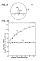
- Test results showing the relative strain of wafers subjected to laser annealing utilizing the "A" type raster of the prior art, as compared with wafers annealed utilizing the "B" type raster scan of this invention, are shown in Figure lg.
- the abscissa of Figure lg shows the distance across the wafer, in millimeters.
- the ordinate of Figure lg shows a measure of the relative strain of the wafer.
- the relative strain of the wafer is measured utilizing well-known techniques for determining the distortion of the wafer, as is measured in microns by a microscopic technique showing the change in depth of focus in the distorted region.
- the wafer which has been laser annealed utilizing the technique of this invention shows virtually no relative strain.
- the wafer which has been laser annealed utilizing the raster scan of the prior art shows considerable relative strain, which results in a tensile stress of approximately 2.9x14 g dynes/cm 2 .
- phosphosilicate glass formed on semiconductor wafers is laser annealed, while generating less strain on the surface of the wafer than in prior art techniques, thus resulting in substantially less damage to the wafer.
Landscapes
- Laser Beam Processing (AREA)
- Recrystallisation Techniques (AREA)
Applications Claiming Priority (2)
| Application Number | Priority Date | Filing Date | Title |
|---|---|---|---|
| US244395 | 1981-03-16 | ||
| US06/244,395 US4415794A (en) | 1981-03-16 | 1981-03-16 | Laser scanning method for annealing, glass flow and related processes |
Publications (3)
| Publication Number | Publication Date |
|---|---|
| EP0061951A2 true EP0061951A2 (fr) | 1982-10-06 |
| EP0061951A3 EP0061951A3 (en) | 1983-09-07 |
| EP0061951B1 EP0061951B1 (fr) | 1987-05-06 |
Family
ID=22922563
Family Applications (1)
| Application Number | Title | Priority Date | Filing Date |
|---|---|---|---|
| EP82400445A Expired EP0061951B1 (fr) | 1981-03-16 | 1982-03-12 | Procédé de balayage par rayon laser pour recuire, couler du verre et procédés semblables |
Country Status (5)
| Country | Link |
|---|---|
| US (1) | US4415794A (fr) |
| EP (1) | EP0061951B1 (fr) |
| JP (1) | JPS57162341A (fr) |
| CA (1) | CA1182931A (fr) |
| DE (1) | DE3276282D1 (fr) |
Cited By (1)
| Publication number | Priority date | Publication date | Assignee | Title |
|---|---|---|---|---|
| CN110216370A (zh) * | 2019-05-17 | 2019-09-10 | 北京华卓精科科技股份有限公司 | 激光退火方法和系统 |
Families Citing this family (15)
| Publication number | Priority date | Publication date | Assignee | Title |
|---|---|---|---|---|
| JPS58176929A (ja) * | 1982-04-09 | 1983-10-17 | Fujitsu Ltd | 半導体装置の製造方法 |
| JPH0616155B2 (ja) * | 1982-10-20 | 1994-03-02 | コニカ株式会社 | 放射線画像読取方法 |
| US6417484B1 (en) * | 1998-12-21 | 2002-07-09 | Micron Electronics, Inc. | Laser marking system for dice carried in trays and method of operation |
| US6675057B2 (en) * | 2001-04-25 | 2004-01-06 | Intel Corporation | Integrated circuit annealing methods and apparatus |
| TW552645B (en) | 2001-08-03 | 2003-09-11 | Semiconductor Energy Lab | Laser irradiating device, laser irradiating method and manufacturing method of semiconductor device |
| KR100885904B1 (ko) * | 2001-08-10 | 2009-02-26 | 가부시키가이샤 한도오따이 에네루기 켄큐쇼 | 레이저 어닐링장치 및 반도체장치의 제작방법 |
| JP4555568B2 (ja) * | 2001-11-09 | 2010-10-06 | 株式会社半導体エネルギー研究所 | レーザ処理装置、レーザ処理方法および薄膜トランジスタの作製方法 |
| US7745762B2 (en) * | 2005-06-01 | 2010-06-29 | Mattson Technology, Inc. | Optimizing the thermal budget during a pulsed heating process |
| US20080173620A1 (en) * | 2005-09-26 | 2008-07-24 | Ultratech, Inc. | Apparatuses and methods for irradiating a substrate to avoid substrate edge damage |
| US8319149B2 (en) * | 2008-04-16 | 2012-11-27 | Applied Materials, Inc. | Radiant anneal throughput optimization and thermal history minimization by interlacing |
| JP2012084620A (ja) * | 2010-10-08 | 2012-04-26 | Mitsubishi Electric Corp | レーザ加工装置 |
| JP5679940B2 (ja) * | 2011-09-29 | 2015-03-04 | 住友重機械工業株式会社 | レーザアニール装置、及びレーザアニール方法 |
| DE102012111698A1 (de) * | 2012-12-03 | 2014-03-20 | Solarworld Innovations Gmbh | Verfahren und Vorrichtung zum Bearbeiten mindestens eines kristallinen Silizium-Wafers oder eines Solarzellen-Wafers |
| US9443726B1 (en) | 2015-03-13 | 2016-09-13 | United Microelectronics Corp. | Semiconductor process |
| JP7734113B2 (ja) * | 2022-05-16 | 2025-09-04 | 住友重機械工業株式会社 | レーザ処理支援装置及びレーザ処理方法 |
Family Cites Families (5)
| Publication number | Priority date | Publication date | Assignee | Title |
|---|---|---|---|---|
| US3900737A (en) * | 1974-04-18 | 1975-08-19 | Bell Telephone Labor Inc | Electron beam exposure system |
| US4131487A (en) * | 1977-10-26 | 1978-12-26 | Western Electric Company, Inc. | Gettering semiconductor wafers with a high energy laser beam |
| US4316074A (en) * | 1978-12-20 | 1982-02-16 | Quantronix Corporation | Method and apparatus for laser irradiating semiconductor material |
| US4234358A (en) * | 1979-04-05 | 1980-11-18 | Western Electric Company, Inc. | Patterned epitaxial regrowth using overlapping pulsed irradiation |
| JPS55150238A (en) * | 1979-05-10 | 1980-11-22 | Matsushita Electric Ind Co Ltd | Method of irradiating laser beam |
-
1981
- 1981-03-16 US US06/244,395 patent/US4415794A/en not_active Expired - Lifetime
-
1982
- 1982-03-12 EP EP82400445A patent/EP0061951B1/fr not_active Expired
- 1982-03-12 DE DE8282400445T patent/DE3276282D1/de not_active Expired
- 1982-03-15 CA CA000398339A patent/CA1182931A/fr not_active Expired
- 1982-03-15 JP JP57039620A patent/JPS57162341A/ja active Granted
Cited By (1)
| Publication number | Priority date | Publication date | Assignee | Title |
|---|---|---|---|---|
| CN110216370A (zh) * | 2019-05-17 | 2019-09-10 | 北京华卓精科科技股份有限公司 | 激光退火方法和系统 |
Also Published As
| Publication number | Publication date |
|---|---|
| JPH0416936B2 (fr) | 1992-03-25 |
| US4415794A (en) | 1983-11-15 |
| JPS57162341A (en) | 1982-10-06 |
| EP0061951B1 (fr) | 1987-05-06 |
| EP0061951A3 (en) | 1983-09-07 |
| DE3276282D1 (en) | 1987-06-11 |
| CA1182931A (fr) | 1985-02-19 |
Similar Documents
| Publication | Publication Date | Title |
|---|---|---|
| US4415794A (en) | Laser scanning method for annealing, glass flow and related processes | |
| US7846847B2 (en) | Method of separating layers of material | |
| US4131487A (en) | Gettering semiconductor wafers with a high energy laser beam | |
| EP0100638B1 (fr) | Traitement d'acier électrique avec un laser | |
| EP0037685B1 (fr) | Procédé de fabrication d'un dispositif semiconducteur | |
| EP0032801A2 (fr) | Procédé pour diviser une plaque semiconductrice | |
| US4179310A (en) | Laser trim protection process | |
| US4443493A (en) | Laser induced flow glass materials | |
| Domke et al. | Ultrafast-laser dicing of thin silicon wafers: strategies to improve front-and backside breaking strength | |
| CA1140683A (fr) | Methode de purification du silicium a rendement eleve par formation de centres de fluide surchauffe | |
| EP0434138A1 (fr) | Méthode de formation d'un conducteur en aluminium avec une structure de grains alignés | |
| US4549064A (en) | Laser treatment of silicon nitride | |
| US4137100A (en) | Forming isolation and device regions due to enhanced diffusion of impurities in semiconductor material by laser | |
| EP0109499B1 (fr) | Traitement à laser de PSG, oxyde et nitride via un recuit par laser par absorption sélective optimalisée | |
| US4431900A (en) | Laser induced flow Ge-O based materials | |
| EP0130847A2 (fr) | Procédé de fabrication d'un dispositif semi-conducteur | |
| US4542037A (en) | Laser induced flow of glass bonded materials | |
| Weinberg | Polysilicon recrystallization by CO2 laser heating of SiO2 | |
| JPS641046B2 (fr) | ||
| Paulson et al. | The influence of dielectric layers on the CW-Laser Annealing of polysilicon | |
| Brown | Laser processing of semiconductors | |
| JPH07321371A (ja) | 受発光ダイオードの形成方法 | |
| GB2112205A (en) | A thermal processing system for semiconductors and other materials using two or more electron beams | |
| Calder et al. | Activation of polysilicon connections by selective CW laser annealing | |
| Lenkkeri et al. | Laser-induced CVD of doped silicon stripes on SOS and their characterization by piezoresistivity measurements |
Legal Events
| Date | Code | Title | Description |
|---|---|---|---|
| PUAI | Public reference made under article 153(3) epc to a published international application that has entered the european phase |
Free format text: ORIGINAL CODE: 0009012 |
|
| AK | Designated contracting states |
Designated state(s): DE FR GB IT NL |
|
| PUAL | Search report despatched |
Free format text: ORIGINAL CODE: 0009013 |
|
| AK | Designated contracting states |
Designated state(s): DE FR GB IT NL |
|
| 17P | Request for examination filed |
Effective date: 19840302 |
|
| GRAA | (expected) grant |
Free format text: ORIGINAL CODE: 0009210 |
|
| ITF | It: translation for a ep patent filed | ||
| AK | Designated contracting states |
Kind code of ref document: B1 Designated state(s): DE FR GB IT NL |
|
| REF | Corresponds to: |
Ref document number: 3276282 Country of ref document: DE Date of ref document: 19870611 |
|
| ET | Fr: translation filed | ||
| PLBE | No opposition filed within time limit |
Free format text: ORIGINAL CODE: 0009261 |
|
| STAA | Information on the status of an ep patent application or granted ep patent |
Free format text: STATUS: NO OPPOSITION FILED WITHIN TIME LIMIT |
|
| 26N | No opposition filed | ||
| GBPC | Gb: european patent ceased through non-payment of renewal fee | ||
| GBPC | Gb: european patent ceased through non-payment of renewal fee |
Free format text: 5204, PAGE 3645 |
|
| GBPC | Gb: european patent ceased through non-payment of renewal fee |
Free format text: 5204, PAGE 3645 |
|
| ITTA | It: last paid annual fee | ||
| PGFP | Annual fee paid to national office [announced via postgrant information from national office to epo] |
Ref country code: GB Payment date: 19940207 Year of fee payment: 13 |
|
| PGFP | Annual fee paid to national office [announced via postgrant information from national office to epo] |
Ref country code: FR Payment date: 19940311 Year of fee payment: 13 |
|
| PGFP | Annual fee paid to national office [announced via postgrant information from national office to epo] |
Ref country code: NL Payment date: 19940331 Year of fee payment: 13 |
|
| PG25 | Lapsed in a contracting state [announced via postgrant information from national office to epo] |
Ref country code: GB Effective date: 19950312 |
|
| PG25 | Lapsed in a contracting state [announced via postgrant information from national office to epo] |
Ref country code: NL Effective date: 19951001 |
|
| GBPC | Gb: european patent ceased through non-payment of renewal fee |
Effective date: 19950312 |
|
| PG25 | Lapsed in a contracting state [announced via postgrant information from national office to epo] |
Ref country code: FR Free format text: LAPSE BECAUSE OF NON-PAYMENT OF DUE FEES Effective date: 19951130 |
|
| NLV4 | Nl: lapsed or anulled due to non-payment of the annual fee |
Effective date: 19951001 |
|
| REG | Reference to a national code |
Ref country code: FR Ref legal event code: ST |
|
| PGFP | Annual fee paid to national office [announced via postgrant information from national office to epo] |
Ref country code: DE Payment date: 20010220 Year of fee payment: 20 |