EP0062097B1 - Verfahren zur Darstellung logischer Zustandsänderungen mehrerer benachbarter Schaltungsknoten in integrierten Schaltungen in einem Logikbild mittels einer gepulsten Elektronensonde - Google Patents
Verfahren zur Darstellung logischer Zustandsänderungen mehrerer benachbarter Schaltungsknoten in integrierten Schaltungen in einem Logikbild mittels einer gepulsten Elektronensonde Download PDFInfo
- Publication number
- EP0062097B1 EP0062097B1 EP81108595A EP81108595A EP0062097B1 EP 0062097 B1 EP0062097 B1 EP 0062097B1 EP 81108595 A EP81108595 A EP 81108595A EP 81108595 A EP81108595 A EP 81108595A EP 0062097 B1 EP0062097 B1 EP 0062097B1
- Authority
- EP
- European Patent Office
- Prior art keywords
- electron
- logic
- scanning
- pulsed
- line
- Prior art date
- Legal status (The legal status is an assumption and is not a legal conclusion. Google has not performed a legal analysis and makes no representation as to the accuracy of the status listed.)
- Expired
Links
- 238000000034 method Methods 0.000 title claims description 15
- 239000000523 sample Substances 0.000 title claims description 13
- 238000010894 electron beam technology Methods 0.000 claims description 7
- 239000004020 conductor Substances 0.000 claims 2
- 230000003252 repetitive effect Effects 0.000 claims 1
- 238000012360 testing method Methods 0.000 description 6
- 238000005259 measurement Methods 0.000 description 5
- 238000003384 imaging method Methods 0.000 description 2
- 238000013507 mapping Methods 0.000 description 2
- 238000005070 sampling Methods 0.000 description 2
- 238000004458 analytical method Methods 0.000 description 1
- 238000013461 design Methods 0.000 description 1
- 238000011161 development Methods 0.000 description 1
- 238000001493 electron microscopy Methods 0.000 description 1
- 238000011835 investigation Methods 0.000 description 1
- 238000012552 review Methods 0.000 description 1
Images
Classifications
-
- G—PHYSICS
- G01—MEASURING; TESTING
- G01R—MEASURING ELECTRIC VARIABLES; MEASURING MAGNETIC VARIABLES
- G01R31/00—Arrangements for testing electric properties; Arrangements for locating electric faults; Arrangements for electrical testing characterised by what is being tested not provided for elsewhere
- G01R31/28—Testing of electronic circuits, e.g. by signal tracer
- G01R31/302—Contactless testing
- G01R31/305—Contactless testing using electron beams
-
- B—PERFORMING OPERATIONS; TRANSPORTING
- B82—NANOTECHNOLOGY
- B82Y—SPECIFIC USES OR APPLICATIONS OF NANOSTRUCTURES; MEASUREMENT OR ANALYSIS OF NANOSTRUCTURES; MANUFACTURE OR TREATMENT OF NANOSTRUCTURES
- B82Y15/00—Nanotechnology for interacting, sensing or actuating, e.g. quantum dots as markers in protein assays or molecular motors
Definitions
- the invention relates to a method for representing the logic states occurring at adjacent circuit nodes of a program-controlled integrated circuit in a two-dimensional logic image.
- the invention describes a method with which it is possible to map logical changes in state on adjacent interconnects, provided that the measuring points of interest lie on a straight line.
- Changes in the state of short interconnects can be measured individually either with mechanical measuring tips or with the electron probe interconnect for interconnect. However, a simultaneous measurement of changes in state on short interconnects is difficult with mechanical measuring tips.
- the invention has for its object to provide a method for displaying logical states of several adjacent circuit nodes in integrated circuits in a logic image by means of a pulsed electron probe in a scanning electron microscope, which can also be used on short pieces of interconnect.
- this object is achieved by a method according to claim 1.
- phase range of a picture run is freely selected.
- the circuit In order to obtain an association between the logic image and the device under test, it is possible for the circuit to be mapped to the scanning line by electron microscopy, and for the line advance of the pulsed electron probe to be interrupted only when this scanning line is reached.
- the image on the screen of the scanning electron microscope shows a section of the integrated circuit in the upper part and, in the subsequent lower part of the screen of the scanning electron microscope, a bar representation of the logical states of the last line of this integrated circuit which is shown in the representation of logical state changes several adjacent circuit nodes in this integrated circuit in a logic image by means of a pulsed electron probe serves as a recording line.
- the information content of the logical state changes of several adjacent circuit nodes in integrated circuits shown in a logic image corresponds to that of a conventional logic analyzer as used for testing microcomputers and computers [J. McLeod, Logic analyzers - sharp faultfinders getting sharper, Electronic Design, 28 (1980) 7, pp. 48-56].
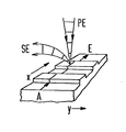
- the figure shows the movement of the pulsed electrode probe when the logic image is generated.
- the logic image technique described here builds on the work cited in the prior art.
- the measuring principle for creating a logic image is described below.
- the experimental investigations were carried out on an unpassivated 8085 microprocessor, which was developed and manufactured in a shrunk version at Siemens.
- the measuring principle for creating a logic image is based on the sampling principle (L. Balk et al., "Quantitative Voltage Contrast at High Frequencies in the SEM", SEM / 1976 pp. 615-624).
- the program loops should be as short as possible, since the pulse-pause ratio in sampling techniques with the electron probe must not be too small [A. Gopinath, "Estimate of minimum measurable voltage in the SEM", J. Phys. E: Sci. instrum., vol. 10, pp. 911-913 (1977)].
- the figure shows schematically how a logic picture is created.
- the pulsed electron probe slowly scans the interconnects in the x direction, of which only two are shown in the picture. once it has reached the end of line E, it jumps back to the start of line A and the process begins again ("line scan").
- the electron beam scans this screen line by line on the screen of the scanning electron microscope, so that an areal image is created on this screen.
- the phase of the electron pulses which slowly scan the interconnects in the x direction, is continuously shifted. Due to the freely selectable phase range during a picture run, either the entire program loop or any part of it can be represented in the logic picture.
- the logical states are represented by the potential contrast: logical «0» appears bright and logically "1" appears dark (A. Gopinath et al, "Voltage Contrast: A Review", SEM / 1978 pp. 375-380 and H.-P. Feuerbaum et al., "Qualitative and quantitative voltage measurement on integrated circuits » Contributions of electron microscopic direct imaging surface, vol. 8 pp. 469-480, 1975).
- PE is the pulsed electron probe and SE the secondary electrodes.
Landscapes
- Engineering & Computer Science (AREA)
- Nanotechnology (AREA)
- Chemical & Material Sciences (AREA)
- General Health & Medical Sciences (AREA)
- Health & Medical Sciences (AREA)
- Life Sciences & Earth Sciences (AREA)
- General Physics & Mathematics (AREA)
- Molecular Biology (AREA)
- Physics & Mathematics (AREA)
- Crystallography & Structural Chemistry (AREA)
- General Engineering & Computer Science (AREA)
- Tests Of Electronic Circuits (AREA)
- Testing Or Measuring Of Semiconductors Or The Like (AREA)
- Measurement Of Current Or Voltage (AREA)
Applications Claiming Priority (2)
| Application Number | Priority Date | Filing Date | Title |
|---|---|---|---|
| DE19813110138 DE3110138A1 (de) | 1981-03-16 | 1981-03-16 | Verfahren zur darstellung logischer zustandsaenderungen mehrerer benachbarter schaltungsknoten in integrierten schaltungen in einem logikbild mittels einer gepulsten elektronensonde |
| DE3110138 | 1981-03-16 |
Publications (2)
| Publication Number | Publication Date |
|---|---|
| EP0062097A1 EP0062097A1 (de) | 1982-10-13 |
| EP0062097B1 true EP0062097B1 (de) | 1985-05-02 |
Family
ID=6127438
Family Applications (1)
| Application Number | Title | Priority Date | Filing Date |
|---|---|---|---|
| EP81108595A Expired EP0062097B1 (de) | 1981-03-16 | 1981-10-20 | Verfahren zur Darstellung logischer Zustandsänderungen mehrerer benachbarter Schaltungsknoten in integrierten Schaltungen in einem Logikbild mittels einer gepulsten Elektronensonde |
Country Status (4)
| Country | Link |
|---|---|
| US (1) | US4471302A (ja) |
| EP (1) | EP0062097B1 (ja) |
| JP (1) | JPH0614101B2 (ja) |
| DE (2) | DE3110138A1 (ja) |
Families Citing this family (8)
| Publication number | Priority date | Publication date | Assignee | Title |
|---|---|---|---|---|
| DE3334494A1 (de) * | 1983-09-23 | 1985-04-11 | Siemens AG, 1000 Berlin und 8000 München | Verfahren zum messen niederfrequenter signalverlaeufe innerhalb integrierter schaltungen mit der elektronensonde |
| EP0166912B1 (de) * | 1984-06-01 | 1990-08-29 | Siemens Aktiengesellschaft | Verfahren zur elektrischen Prüfung von Mikroverdrahtungen mit Hilfe von Korpuskularsonden |
| FR2592958B1 (fr) * | 1986-01-14 | 1988-05-13 | Matra | Procede et dispositif d'analyse de composants electroniques en contraste de potentiel. |
| US4749947A (en) * | 1986-03-10 | 1988-06-07 | Cross-Check Systems, Inc. | Grid-based, "cross-check" test structure for testing integrated circuits |
| NL8700933A (nl) * | 1987-04-21 | 1988-11-16 | Philips Nv | Testmethode voor lcd-elementen. |
| US4902963A (en) * | 1988-01-28 | 1990-02-20 | Brust Hans D | Method and arrangement for recording periodic signals with a laser probe |
| US5065090A (en) * | 1988-07-13 | 1991-11-12 | Cross-Check Technology, Inc. | Method for testing integrated circuits having a grid-based, "cross-check" te |
| EP0392035B1 (de) * | 1989-04-11 | 1994-06-22 | ICT Integrated Circuit Testing Gesellschaft für HalbleiterprÀ¼ftechnik mbH | Verfahren zur Aufzeichnung oder Abbildung zeitabhängiger Potentiale in Bauelementen der Mikroelektronik |
Family Cites Families (4)
| Publication number | Priority date | Publication date | Assignee | Title |
|---|---|---|---|---|
| DE2813948A1 (de) * | 1978-03-31 | 1979-10-11 | Siemens Ag | Verfahren zur elektronischen abbildung der potentialverteilung in einem elektronischen bauelement |
| DE2813947C2 (de) * | 1978-03-31 | 1986-09-04 | Siemens AG, 1000 Berlin und 8000 München | Verfahren zur berührungslosen Messung des Potentialverlaufs in einem elektronischen Bauelement und Anordnung zur Durchführung des Verfahrens |
| DE2814049A1 (de) * | 1978-03-31 | 1979-10-18 | Siemens Ag | Verfahren zur beruehrungslosen messung des potentialverlaufs in einem elektronischen bauelement und anordnung zur durchfuehrung des verfahrens |
| DE2903077C2 (de) * | 1979-01-26 | 1986-07-17 | Siemens AG, 1000 Berlin und 8000 München | Verfahren zur berührungslosen Potentialmessung an einem elektronischen Bauelement und Anordnung zur Durchführung des Verfahrens |
-
1981
- 1981-03-16 DE DE19813110138 patent/DE3110138A1/de not_active Withdrawn
- 1981-10-20 DE DE8181108595T patent/DE3170325D1/de not_active Expired
- 1981-10-20 EP EP81108595A patent/EP0062097B1/de not_active Expired
-
1982
- 1982-01-20 US US06/341,106 patent/US4471302A/en not_active Expired - Lifetime
- 1982-03-16 JP JP57041613A patent/JPH0614101B2/ja not_active Expired - Lifetime
Non-Patent Citations (6)
| Title |
|---|
| Beitr. elektronenmikroskop. Direkt-abb. Oberfl. 11 (1978) S. 67-71 * |
| Beitr. elektronenmikroskop. Direkt-abb. Oberfl. 8 (1975) S. 469-480 * |
| Digest of papers 1980 IEEE Test Conference S. 444-449 * |
| J. Phys. E: Sci.Instr. vol. 10(1977) S. 911-913 * |
| SEM (1976) S. 615-624 * |
| SEM (1978) S. 375-380 * |
Also Published As
| Publication number | Publication date |
|---|---|
| EP0062097A1 (de) | 1982-10-13 |
| JPH0614101B2 (ja) | 1994-02-23 |
| JPS57173762A (en) | 1982-10-26 |
| US4471302A (en) | 1984-09-11 |
| DE3110138A1 (de) | 1982-09-23 |
| DE3170325D1 (en) | 1985-06-05 |
Similar Documents
| Publication | Publication Date | Title |
|---|---|---|
| DE4026295C2 (ja) | ||
| EP0060321B1 (de) | Verfahren für eine rasche interne Logikprüfung an integrierten Schaltungen | |
| DE68914178T2 (de) | Elektroumstrahlprüfung von elektronischen Komponenten. | |
| EP0104577A1 (de) | Verfahren zur kontaktlosen Prüfung eines Objekts, insbesondere von Mikroverdrahtungen, mit einer Korpuskularstrahl-Sonde | |
| DE3326336A1 (de) | Logikmesseinheit | |
| DE4433733A1 (de) | IC-Analysesystem mit einer Ladungsteilchenstrahlvorrichtung | |
| DE19525536A1 (de) | Verfahren und Vorrichtung zur Feststellung eines Fehlers in einem IC unter Verwendung eines Strahls geladener Teilchen | |
| EP0048858B1 (de) | Vorrichtung zur Signalverarbeitung für ein Elektronenstrahl-Messgerät | |
| DE102004015023B4 (de) | Augendiagramm-Analysator und Verfahren zum Ermitteln von Zeit-Spannungs-Meßpunkten für die Augendiagramm-Analyse | |
| EP0062097A1 (de) | Verfahren zur Darstellung logischer Zustandsänderungen mehrerer benachbarter Schaltungsknoten in integrierten Schaltungen in einem Logikbild mittels einer gepulsten Elektronensonde | |
| EP0497994A1 (de) | Verfahren und Schaltungsanordnung zur Überwachung von ionen- oder redoxpotential-sensitiven Messketten | |
| EP0075710A1 (de) | Abtastverfahren zur Potentialbestimmung in der Elektronenstrahl-Messtechnik | |
| EP0136591B1 (de) | Verfahren zum Messen niederfrequenter Signalverläufe innerhalb integrierter Schaltungen mit der Elektronensonde | |
| EP0166815A1 (de) | Verfahren und Vorrichtung zur Spektralanalyse eines Signals an einem Messpunkt | |
| EP0125329B1 (de) | Messwandler auf der Basis des elektro- bzw. magnetooptischen Effektes | |
| DE3331458A1 (de) | Signalanalysator | |
| EP0060924B1 (de) | Selektives Logikbild von Informationsgruppen auf mehreren zusammengehörenden Knoten einer integrierten Schaltung | |
| EP0060925B1 (de) | Aufzeichnung von sich nicht zyklisch wiederholenden logischen Zustandsänderungen an einer Messstelle im Inneren von integrierten Schaltungen mit der Elektronensonde | |
| DE102009022965A1 (de) | Messung eines Substrats mit elektrisch leitenden Strukturen | |
| DE69319542T2 (de) | Apparat zum Messen der Verteilung eines elektromagnetischen Feldes mit einem fokussierten Elektronenstrahl | |
| DE3308717A1 (de) | Vorrichtung zum ausmessen von magnetfeldern | |
| DE1930663B2 (de) | Verfahren zur Aufzeichnung der Deformation von Materialproben und Vorrichtung zur Durchführung dieses Verfahrens | |
| DE4023387A1 (de) | Verfahren zur probenschonenden erzeugung eines logikbildes | |
| DE69900869T2 (de) | Verfahren und Vorrichtung zur Prüfung eines elektronischen Bauteils | |
| DE2037157A1 (de) | Einrichtung zur Messung der Dielektn zitatskonstante von Stoffen |
Legal Events
| Date | Code | Title | Description |
|---|---|---|---|
| PUAI | Public reference made under article 153(3) epc to a published international application that has entered the european phase |
Free format text: ORIGINAL CODE: 0009012 |
|
| 17P | Request for examination filed |
Effective date: 19811020 |
|
| AK | Designated contracting states |
Designated state(s): DE FR GB NL |
|
| GRAA | (expected) grant |
Free format text: ORIGINAL CODE: 0009210 |
|
| AK | Designated contracting states |
Designated state(s): DE FR GB NL |
|
| REF | Corresponds to: |
Ref document number: 3170325 Country of ref document: DE Date of ref document: 19850605 |
|
| ET | Fr: translation filed | ||
| PLBE | No opposition filed within time limit |
Free format text: ORIGINAL CODE: 0009261 |
|
| STAA | Information on the status of an ep patent application or granted ep patent |
Free format text: STATUS: NO OPPOSITION FILED WITHIN TIME LIMIT |
|
| 26N | No opposition filed | ||
| NLS | Nl: assignments of ep-patents |
Owner name: ICT INTEGRATED CIRCUIT TESTING GESELLSCHAFT FUER H |
|
| REG | Reference to a national code |
Ref country code: FR Ref legal event code: TP |
|
| REG | Reference to a national code |
Ref country code: GB Ref legal event code: 732 |
|
| PGFP | Annual fee paid to national office [announced via postgrant information from national office to epo] |
Ref country code: NL Payment date: 19911031 Year of fee payment: 11 |
|
| PG25 | Lapsed in a contracting state [announced via postgrant information from national office to epo] |
Ref country code: NL Effective date: 19930501 |
|
| NLV4 | Nl: lapsed or anulled due to non-payment of the annual fee | ||
| REG | Reference to a national code |
Ref country code: FR Ref legal event code: TP |
|
| REG | Reference to a national code |
Ref country code: GB Ref legal event code: 732E |
|
| REG | Reference to a national code |
Ref country code: GB Ref legal event code: 732E |
|
| REG | Reference to a national code |
Ref country code: FR Ref legal event code: TP |
|
| REG | Reference to a national code |
Ref country code: GB Ref legal event code: 732E |
|
| REG | Reference to a national code |
Ref country code: FR Ref legal event code: TP |
|
| PGFP | Annual fee paid to national office [announced via postgrant information from national office to epo] |
Ref country code: FR Payment date: 20000911 Year of fee payment: 20 |
|
| PGFP | Annual fee paid to national office [announced via postgrant information from national office to epo] |
Ref country code: GB Payment date: 20000919 Year of fee payment: 20 |
|
| PGFP | Annual fee paid to national office [announced via postgrant information from national office to epo] |
Ref country code: DE Payment date: 20001222 Year of fee payment: 20 |
|
| PG25 | Lapsed in a contracting state [announced via postgrant information from national office to epo] |
Ref country code: GB Free format text: LAPSE BECAUSE OF EXPIRATION OF PROTECTION Effective date: 20011019 |
|
| REG | Reference to a national code |
Ref country code: GB Ref legal event code: PE20 Effective date: 20011019 |